EP0651273A1 - Mikromechanischer optischer Verschluss - Google Patents
Mikromechanischer optischer Verschluss Download PDFInfo
- Publication number
- EP0651273A1 EP0651273A1 EP94116985A EP94116985A EP0651273A1 EP 0651273 A1 EP0651273 A1 EP 0651273A1 EP 94116985 A EP94116985 A EP 94116985A EP 94116985 A EP94116985 A EP 94116985A EP 0651273 A1 EP0651273 A1 EP 0651273A1
- Authority
- EP
- European Patent Office
- Prior art keywords
- rotor
- array
- vias
- substrate
- shutter
- Prior art date
- Legal status (The legal status is an assumption and is not a legal conclusion. Google has not performed a legal analysis and makes no representation as to the accuracy of the status listed.)
- Withdrawn
Links
- 230000003287 optical effect Effects 0.000 title claims description 24
- 239000000758 substrate Substances 0.000 claims abstract description 34
- 238000000034 method Methods 0.000 claims abstract description 28
- 238000004519 manufacturing process Methods 0.000 claims abstract description 24
- 230000005855 radiation Effects 0.000 claims abstract description 7
- 239000000463 material Substances 0.000 claims description 22
- 238000005530 etching Methods 0.000 claims description 18
- 239000013307 optical fiber Substances 0.000 claims description 11
- 230000000903 blocking effect Effects 0.000 claims description 4
- 238000000151 deposition Methods 0.000 claims description 4
- 229910052710 silicon Inorganic materials 0.000 claims description 4
- 239000010703 silicon Substances 0.000 claims description 4
- 230000001131 transforming effect Effects 0.000 claims 2
- 239000000835 fiber Substances 0.000 description 6
- 125000006850 spacer group Chemical group 0.000 description 6
- 238000013461 design Methods 0.000 description 4
- XUIMIQQOPSSXEZ-UHFFFAOYSA-N Silicon Chemical compound [Si] XUIMIQQOPSSXEZ-UHFFFAOYSA-N 0.000 description 3
- 238000003491 array Methods 0.000 description 3
- 230000000875 corresponding effect Effects 0.000 description 3
- 229920002120 photoresistant polymer Polymers 0.000 description 3
- 230000000873 masking effect Effects 0.000 description 2
- 238000012986 modification Methods 0.000 description 2
- 230000004048 modification Effects 0.000 description 2
- 229910052581 Si3N4 Inorganic materials 0.000 description 1
- 229910021417 amorphous silicon Inorganic materials 0.000 description 1
- 230000001276 controlling effect Effects 0.000 description 1
- 230000002596 correlated effect Effects 0.000 description 1
- 230000007423 decrease Effects 0.000 description 1
- 230000008021 deposition Effects 0.000 description 1
- 238000011161 development Methods 0.000 description 1
- 229910021421 monocrystalline silicon Inorganic materials 0.000 description 1
- TWNQGVIAIRXVLR-UHFFFAOYSA-N oxo(oxoalumanyloxy)alumane Chemical compound O=[Al]O[Al]=O TWNQGVIAIRXVLR-UHFFFAOYSA-N 0.000 description 1
- 239000005365 phosphate glass Substances 0.000 description 1
- 238000012545 processing Methods 0.000 description 1
- 239000010453 quartz Substances 0.000 description 1
- 239000004065 semiconductor Substances 0.000 description 1
- VYPSYNLAJGMNEJ-UHFFFAOYSA-N silicon dioxide Inorganic materials O=[Si]=O VYPSYNLAJGMNEJ-UHFFFAOYSA-N 0.000 description 1
- HQVNEWCFYHHQES-UHFFFAOYSA-N silicon nitride Chemical compound N12[Si]34N5[Si]62N3[Si]51N64 HQVNEWCFYHHQES-UHFFFAOYSA-N 0.000 description 1
- 238000004544 sputter deposition Methods 0.000 description 1
- 238000005728 strengthening Methods 0.000 description 1
Images


Classifications
-
- G—PHYSICS
- G02—OPTICS
- G02B—OPTICAL ELEMENTS, SYSTEMS OR APPARATUS
- G02B26/00—Optical devices or arrangements for the control of light using movable or deformable optical elements
- G02B26/02—Optical devices or arrangements for the control of light using movable or deformable optical elements for controlling the intensity of light
- G02B26/04—Optical devices or arrangements for the control of light using movable or deformable optical elements for controlling the intensity of light by periodically varying the intensity of light, e.g. using choppers
-
- H—ELECTRICITY
- H02—GENERATION; CONVERSION OR DISTRIBUTION OF ELECTRIC POWER
- H02N—ELECTRIC MACHINES NOT OTHERWISE PROVIDED FOR
- H02N1/00—Electrostatic generators or motors using a solid moving electrostatic charge carrier
- H02N1/002—Electrostatic motors
- H02N1/004—Electrostatic motors in which a body is moved along a path due to interaction with an electric field travelling along the path
Definitions
- This invention relates to micro-optical devices, and more particularly, to an optical shutter whose motion is provided by a micromotor.
- micro-optical devices use tiny optical components for applications such as lightwave communications and optical computing.
- An example of a micro-optical device is a microlens array, which can be fabricated using integrated circuit fabrication techniques.
- Various guided wave devices, such as planar waveguides are also being made on a micro-optical scale.
- a first aspect of the invention is an array of micro-optical shutters, each for intermittently blocking the passage of radiation.
- a substrate has a plurality of vias through which said radiation may pass.
- Each via is associated with a shutter which is capable of rotating.
- each shutter comprises a rotor hub fabricated on the substrate and a rotor spaced above the substrate for revolving around the rotor hub in a plane parallel to the substrate, The rotor has at least one opening that is aligned with the via during a part of each revolution of the rotor.
- a set of stator poles is also fabricated above the substrate around the perimeter of the rotor and substantially co-planar to the rotor.
- a voltage applied to the stator poles provides a rotor torque that causes the rotor to rotate.
- a control unit controls the timing of the voltage applied to the stator poles.
- a technical advantage of the shutter array is that each shutter permits a very small beam of light to be chopped or switched.
- the shutters can be operated at very high speeds, either in continuous or stepped motion. Shutters having continuous motion are useful as infrared choppers. Shutters having stepped motion are useful for optical switching.
- Arrays of shutters can be easily manufactured, each shutter having uniformity of size and of other characteristics. The arrays are especially suited for various applications involving other micro-optical or micro-electrical components, such as optical fibers, lens, and light modulators.
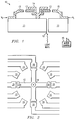
- Figures 1 and 2 are cross sectional and plan views, respectively, of an optical shutter.
- Figures 3A - 3C illustrates the steps of making a via during fabrication of a micromotor.
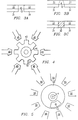
- Figure 4 is an alternative design for the rotor and stator poles.
- Figure 5 is a third alternative design for the rotor.
- Figure 6 illustrates how the rotor geometry determines the duty cycle of blocked versus non-blocked light.
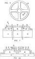
- Figure 7 illustrates a rotor having dished-out portions of its underside for improving the shutter's light blocking capability.
- Figures 8A - 8E illustrate how the fabrication process may be modified to add a filter over the via.
- Figure 9 illustrates an optical correlator that uses an array of optical shutters.
- Figure 10 illustrates an optical switch that uses an array of optical shutters.
- FIGS 1 and 2 are a cross sectional view and a plan view, respectively, of an optical shutter 10 in accordance with the invention.
- Shutter 10 is a "micro-mechanical" device, having dimensions in the order of 100 microns in diameter and thickness.
- Shutter 10 is fabricated on a substrate 11, using semiconductor fabrication techniques, discussed in further detail below. The use of these fabrication techniques permits batch fabrication of many such shutters 10 on a single substrate 11. After fabrication, the shutters may be separated into multi-element arrays, or may be separated into single units.
- substrate 11 is silicon, but may be any material that permits a via 12 to be etched through it.
- suitable materials for substrate 11 are quartz or forms of aluminum oxide. The requirements for the material are that it survive the fabrication process, have sufficient adhesion to the layers deposited over it so as to permit etching, and have etching selectivity with respect to sacrificial materials used during the fabrication process.
- Via 12 extends through substrate 11. As explained below, via 12 permits light from a source to pass upwardly through substrate 11, from bottom to top, where it is intermittently blocked by a rotating rotor 13. Typically, as shown in Figure 2, via 12 is cylindrical in shape.
- via 12 might have a diameter ranging from 2 microns to 50 microns.
- a feature of the invention is that via 12 may be sized so that it securely holds an optical fiber.
- shutter 10 has one via 12 for providing a single point source of light.
- shutter 10 may have more than one via 12.
- Shutter 10 has a rotor 13, which is free to rotate around a hub 14.
- rotor 13 has four equidistant spokes 13a radially extending from an inner ring.
- Spokes 13a are rotor poles, spaced ninety degrees apart.
- a voltage is applied to a stator pole 15
- an electrostatic attractive develops between that stator pole 15 and the nearest rotor pole 13a.
- Timing of the applied voltage to successive stator poles 15 causes a rotor torque on successive rotor poles 13a.
- rotor poles 13a and stator poles 15 are made from a polarizable material, typically silicon.
- Stator poles 15 surround the outer circumference of rotor 13. Each stator pole 15 is connected to a conductive lead (not shown), which permits a voltage to be applied to each stator pole 15.
- motor control unit 16 controls the timing of the applied voltage.
- Control unit 16 may be fabricated on-chip or may be an off-chip component.
- the combination of rotor 13, hub 14, and stators 15 comprise a "micro-motor", whose manufacture is known in the art of micro-mechanics.
- An example of a micro-motor suitable for use with the present invention and a method of manufacture are described in U.S. Patent No. 5,252,881, entitled “Micro Motors and Method for Their Fabrication", which is incorporated by reference herein.
- the rotation of rotor 13 may be continuous or stepped.
- U.S. Patent No. 4,740,410 entitled “Micromechanical Elements and Methods for Their Fabrication” also describes the operation and manufacture of micromotors, and is also incorporated by reference herein.
- Figures 3A - 3C illustrate how known processes for manufacturing a micromotor can be modified to include the opening of via 12 in substrate 11.
- a masking layer 31 is patterned on either side of substrate 11.
- this step has been performed on the underside of substrate 11.
- etching is performed on the patterned side, to etch out via 12.
- the etching results in a cylindrical shaped via 12, especially suitable when via 12 is to hold an optical fiber.
- FIG 3B illustrates a variation of the etching process, which is especially suitable when shutter 10 will be used with a light source other than an optical fiber inserted in via 12.
- the etching is a process known as orientation directed etching (ODE).
- substrate 11 is a material known as 1,1,1 silicon.
- the mask 31 is patterned so that the edges that define via 12 are calculated to result in a via having a desired depth.
- the ODE etches along the single crystal silicon planes.
- the etch results in a cone-shaped via 12.
- a lens directing light toward the underside of shutter 10 may be used to focus light to the "far" opening of via 12.
- via 12 is plugged with a spacer material 32 that will subsequently be removed.
- via 12 may be plugged by depositing a layer of phosphate glass, silicon nitride, or amorphous silicon.
- the masking material 31 may be removed at this time or during some subsequent clean-up phase.
- via 12 is etched and plugged, the layers for the rotor 13, hub 14, and stator 15 are deposited on the top side of substrate 11. Fabrication of these various components is at appropriate locations with respect to via 12. Consistent with known micro-motor fabrication techniques, sublayers of substrate 11 may be deposited for purposes such as strengthening or grounding. Upon completion of rotor 13, hub 14, and stators 15, an etching step removes the spacer material that fills via 12.
- via 12 would be etched from the underside of substrate 11.
- Appropriate sacrificial material would be deposited over and between rotor 12 and stators 15 for protection during the etching of via 12.
- stator poles 15 may be connected for three-phase operation. Adjacent stator poles 15 are designated as phase one, phase two, and phase three poles. For the twelve stator poles 15 of Figure 2, there are four poles 15 for each phase. The stator poles 15 are connected to a control unit 16 and a voltage applied in successive phases. As each phase rises to its maximum voltage, the stator poles 15 create a force on each rotor arm 13a. The result is a rotor torque, which causes rotor 13 to turn.
- FIG. 4 illustrates an alternative rotor 43 and stator poles 45, especially suitable for stepping, as opposed to continuous rotation. Stepping motion is used when shutter 10 is operated as an optical switch. Like rotor 13, rotor 43 has arms, which are located with respect to via 12 so as to intermittently block light as rotor 43 turns. In this configuration, there are eight rotor poles 43a and six stator poles 45. The applied voltage is applied successively to opposing stator poles 45. As stepping of the voltage from stator poles 45 to a next stator pole 45 occurs, the rotor 43 revolves in a stepped motion around hub 44. For a stepped motor, a DC bias may be applied between the rotor 43 and the substrate 11 when rotor 43 is in a light-blocking phase of its motion, so as to seat rotor 43 against substrate 11.
- FIG. 5 illustrates a third type of rotor 53, which is known as a "wobble" rotor.
- Rotor 53 is designed for continuous motion, but may be disk-shaped, as opposed to having rotor arms.
- Rotor 53 turns around a hub 54, due to torque from applied voltage to stator poles 55.
- the rotation of rotor 53 is eccentric with respect to hub 54.
- An opening in rotor 53 has been etched to permit light from via 12 to pass past rotor 53 as it rotates.
- Figures 2, 4 and 5 illustrate that for both continuous and stepper operation, various rotor geometries may be used. Techniques known in the art of micro-motors may be used for various rotor designs optimized for speed, smoothness of motion, torque, and other motor characteristics.
- Figure 6 illustrates how the rotor geometry is related to a desired duty cycle of blocked versus non-blocked light, regardless of whether the rotor is disk-shaped or spoked.
- Rotor 63 has spokes like the rotors of Figures 2 and 4, but the addition of an outer rim makes it similar to the "wobble" rotor of Figure 5.
- the openings between spokes determine when rotor 63 will block light from via 12 as it revolves.
- a common characteristic of the various rotor designs is that each rotor has at least one opening that permits light from via 12 to pass during part of each revolution.
- Figures 2, 4, and 5 further illustrate that by having a plurality of openings in the rotor, the frequency of blocked versus non-blocked light can be increased without increasing the speed of rotation.
- rotor 13 has four openings, for each revolution, light from via 12 is switched from off to on four times.
- Figure 7 illustrates how the fabrication process may be modified to enhance the light blocking capability of shutter 10.
- a number of vias 12 are etched. These vias 12 are etched after rotor 73 and stators 75 are formed. A layer of sacrificial material 76 has been deposited over rotor 73 and stators 75.
- the spacer material is then deposited to plug vias 12. The rest of the fabrication is performed as explained above, with at least one via 12 being unplugged during a final etch. The result is a reflective surface when the rotor 13 blocks light from that via 12.
- Figures 8A - 8E illustrate additional steps in the fabrication process, for adding a filter over one opening of a rotor 83. These steps occur after rotor 83 has been formed, and may occur after hub 84 and stators 85 are formed.
- material has been deposited and etched to form hub 84 and stators 85, as well as rotor 83. All steps except a final cleanup to remove spacer material 66 have been performed.
- Figure 8B is a top plan view of rotor 83 showing that it has two openings.
- a layer of photoresist material 86 has been deposited over rotor 83, and has been etched to form an opening over one of the openings in rotor 83.
- a filter material 88 has been deposited in the opening of the photoresist layer 86.
- the filter material 88 has properties such that it decreases the intensity or affects the color of light transmitted through it.
- the photoresist layer 86 and the spacer layer 66 have been cleaned away, leaving a filter 88 over the opening.
- filter 88 is formed over a larger of two openings in rotor 83.
- the relative sizes of the openings are designed so that the mass added by filter 88 will not substantially unbalance the rotation of rotor 83.
- the smaller size of the unfiltered opening adds mass to that opening.
- a shutter 10 having a rotor 83 with a filter 88 over a first opening and an unfiltered second opening can be operated as a two state shutter, i.e, filtered or non filtered output. Or, it could be operated as a three state shutter, i.e., off, on, or filtered output.
- Figure 9 illustrates an optical correlation system 90, which includes an array 92 of optical shutters 10 in accordance with the invention.
- array 92 provides a plurality of point sources of light, which can be selectively switched on and off. This switching permits a number of different reference views of an object to be compared to an acquired image.
- a number of reference views of the object from different azimuths and elevations could be compared with an image acquired by a surveillance aircraft. It has been experimentally determined that two views of the same object from angles 5 azimuthal degrees apart will correlate with reasonable accuracy.
- the reference images might comprise 72 (360/5) views of the object as seen from different angles on the ground, as well as elevational views if viewing might also be from above.
- a first array of lenses 91 focuses light from a source (not shown) to the shutter array 92, each lens focussing light to each shutter.
- the via 12 of each shutter 10 is cone- shaped, as described above in connection with Figure 3B, so that the lenses of array 91 can focus light to the far opening of each via 12.
- an optical fiber could be inserted into each via 12 of each shutter 10. Typically, these optical fibers would originate from a common light source.
- the shutters of the array 92 are controlled by a control unit 92a so that a single shutter is open at one time.
- the light from the source is directed through that shutter and to a corresponding lens of a second lens array 93, which collimates the light.
- the collimated light passes through a corresponding reference image of the reference film 94.
- the light that is transmitted through the reference image is scaled and Fourier transformed by transform lens 95.
- a spatial light modulator 97 displays an image representing the complex conjugate of the Fourier transform of the acquired image, F*(u,v).
- the transformed reference image illuminates the face of the SLM 97. The result is that the total light reflected from SLM 97 is the product of the Fourier transform of the reference image and the complex conjugate of the Fourier transform of the acquired image.
- This combined image is directed, via a beam splitter 96, to a second Fourier transform lens 98.
- the resulting image is incident on a sensor 99.
- the image data acquired from sensor 99 is processed to determine a correlation factor.
- each shutter of array 92 is successively opened.
- a determination is made whether the corresponding image of reference film 94 matches the acquired image. This process continues until a match is found or until it is determined that there is no match.
- FIG. 10 illustrates how an array 102 of optical shutters 10 can be used as an optical switch 100.
- Each shutter 10 has an input optical fiber 104 and an output optical fiber 106. For purposes of illustration, only one row of input fibers 104 and one column of output fibers 106 are shown.
- light from an input fiber 102 can be turned on or off.
- the array can thus be used to communicate a code of data to output fibers 106.
- the shutter array of Figure 10 could also be used to direct light from one channel to another, such as with a crossbar switch.
- each column of input fibers 104 could be from a single source channel, and each row of output fibers 106 could feed a single output channel.
Landscapes
- Physics & Mathematics (AREA)
- General Physics & Mathematics (AREA)
- Optics & Photonics (AREA)
- Mechanical Light Control Or Optical Switches (AREA)
- Micromachines (AREA)
- Exposure And Positioning Against Photoresist Photosensitive Materials (AREA)
- Exposure Of Semiconductors, Excluding Electron Or Ion Beam Exposure (AREA)
Applications Claiming Priority (2)
| Application Number | Priority Date | Filing Date | Title |
|---|---|---|---|
| US08/148,073 US5459602A (en) | 1993-10-29 | 1993-10-29 | Micro-mechanical optical shutter |
| US148073 | 1993-10-29 |
Publications (1)
| Publication Number | Publication Date |
|---|---|
| EP0651273A1 true EP0651273A1 (de) | 1995-05-03 |
Family
ID=22524141
Family Applications (1)
| Application Number | Title | Priority Date | Filing Date |
|---|---|---|---|
| EP94116985A Withdrawn EP0651273A1 (de) | 1993-10-29 | 1994-10-27 | Mikromechanischer optischer Verschluss |
Country Status (4)
| Country | Link |
|---|---|
| US (1) | US5459602A (de) |
| EP (1) | EP0651273A1 (de) |
| JP (1) | JPH07234366A (de) |
| KR (1) | KR950012086A (de) |
Cited By (7)
| Publication number | Priority date | Publication date | Assignee | Title |
|---|---|---|---|---|
| FR2823860A1 (fr) * | 2001-04-23 | 2002-10-25 | Commissariat Energie Atomique | Commutateur optique multivoie |
| GB2379746A (en) * | 2001-09-18 | 2003-03-19 | Marconi Caswell Ltd | Shutter assembly for telecommunication networks |
| EP1557709A1 (de) * | 2004-01-23 | 2005-07-27 | Seiko Epson Corporation | Vorrichtung und Verfahren zur Pixelgenerierung, Vorrichtung und Verfahren zur Bildprojektion |
| EP2131236A1 (de) | 2008-06-03 | 2009-12-09 | Olympus Corporation | Stapelstruktur, Lichtsteuerungsvorrichtung und Herstellungsverfahren für eine Stapelstruktur |
| EP2639620A1 (de) * | 2012-03-15 | 2013-09-18 | BlackBerry Limited | Linsenbasiertes optisches Bildvergrößerungsfenster mit echtem Zwischenbild |
| US8643950B2 (en) | 2012-03-15 | 2014-02-04 | Blackberry Limited | Lens-based image augmenting optical window with intermediate real image |
| US8953245B2 (en) | 2012-03-15 | 2015-02-10 | Blackberry Limited | Lens-based optical window with intermediate real image |
Families Citing this family (189)
| Publication number | Priority date | Publication date | Assignee | Title |
|---|---|---|---|---|
| US6674562B1 (en) | 1994-05-05 | 2004-01-06 | Iridigm Display Corporation | Interferometric modulation of radiation |
| US5642456A (en) * | 1993-09-14 | 1997-06-24 | Cogent Light Technologies, Inc. | Light intensity attenuator for optical transmission systems |
| US6680792B2 (en) | 1994-05-05 | 2004-01-20 | Iridigm Display Corporation | Interferometric modulation of radiation |
| US7460291B2 (en) | 1994-05-05 | 2008-12-02 | Idc, Llc | Separable modulator |
| US8014059B2 (en) | 1994-05-05 | 2011-09-06 | Qualcomm Mems Technologies, Inc. | System and method for charge control in a MEMS device |
| US7297471B1 (en) | 2003-04-15 | 2007-11-20 | Idc, Llc | Method for manufacturing an array of interferometric modulators |
| US7550794B2 (en) | 2002-09-20 | 2009-06-23 | Idc, Llc | Micromechanical systems device comprising a displaceable electrode and a charge-trapping layer |
| US7138984B1 (en) | 2001-06-05 | 2006-11-21 | Idc, Llc | Directly laminated touch sensitive screen |
| US7123216B1 (en) | 1994-05-05 | 2006-10-17 | Idc, Llc | Photonic MEMS and structures |
| US5699130A (en) * | 1994-05-17 | 1997-12-16 | Taylor Group Of Companies, Inc. | Digital video and audio systems using nano-mechanical structures |
| US5825529A (en) * | 1996-06-27 | 1998-10-20 | Xerox Corporation | Gyricon display with no elastomer substrate |
| US5754332A (en) * | 1996-06-27 | 1998-05-19 | Xerox Corporation | Monolayer gyricon display |
| US6055091A (en) * | 1996-06-27 | 2000-04-25 | Xerox Corporation | Twisting-cylinder display |
| US5914805A (en) * | 1996-06-27 | 1999-06-22 | Xerox Corporation | Gyricon display with interstitially packed particles |
| US5922268A (en) * | 1997-10-30 | 1999-07-13 | Xerox Corporation | Method of manufacturing a twisting cylinder display using multiple chromatic values |
| US5904790A (en) * | 1997-10-30 | 1999-05-18 | Xerox Corporation | Method of manufacturing a twisting cylinder display using multiple chromatic values |
| US5894367A (en) * | 1996-09-13 | 1999-04-13 | Xerox Corporation | Twisting cylinder display using multiple chromatic values |
| US7471444B2 (en) | 1996-12-19 | 2008-12-30 | Idc, Llc | Interferometric modulation of radiation |
| US5929542A (en) * | 1997-02-03 | 1999-07-27 | Honeywell Inc. | Micromechanical stepper motor |
| US5900192A (en) * | 1998-01-09 | 1999-05-04 | Xerox Corporation | Method and apparatus for fabricating very small two-color balls for a twisting ball display |
| US5976428A (en) * | 1998-01-09 | 1999-11-02 | Xerox Corporation | Method and apparatus for controlling formation of two-color balls for a twisting ball display |
| US5990473A (en) * | 1998-02-04 | 1999-11-23 | Sandia Corporation | Apparatus and method for sensing motion in a microelectro-mechanical system |
| US8928967B2 (en) | 1998-04-08 | 2015-01-06 | Qualcomm Mems Technologies, Inc. | Method and device for modulating light |
| WO1999052006A2 (en) | 1998-04-08 | 1999-10-14 | Etalon, Inc. | Interferometric modulation of radiation |
| US7532377B2 (en) | 1998-04-08 | 2009-05-12 | Idc, Llc | Movable micro-electromechanical device |
| US6201633B1 (en) | 1999-06-07 | 2001-03-13 | Xerox Corporation | Micro-electromechanical based bistable color display sheets |
| WO2003007049A1 (en) | 1999-10-05 | 2003-01-23 | Iridigm Display Corporation | Photonic mems and structures |
| US6440252B1 (en) | 1999-12-17 | 2002-08-27 | Xerox Corporation | Method for rotatable element assembly |
| US6545671B1 (en) | 2000-03-02 | 2003-04-08 | Xerox Corporation | Rotating element sheet material with reversible highlighting |
| US6325554B1 (en) | 2000-03-15 | 2001-12-04 | Eastman Kodak Company | Camera with electrostatic light valve that functions as image reflecting mirror for viewfinder |
| US6443637B1 (en) | 2000-03-15 | 2002-09-03 | Eastman Kodak Company | Camera with electrostatic light valve that functions as diaphragm |
| US6498674B1 (en) | 2000-04-14 | 2002-12-24 | Xerox Corporation | Rotating element sheet material with generalized containment structure |
| US6504525B1 (en) | 2000-05-03 | 2003-01-07 | Xerox Corporation | Rotating element sheet material with microstructured substrate and method of use |
| US6402969B1 (en) * | 2000-08-15 | 2002-06-11 | Sandia Corporation | Surface—micromachined rotatable member having a low-contact-area hub |
| US6847347B1 (en) | 2000-08-17 | 2005-01-25 | Xerox Corporation | Electromagnetophoretic display system and method |
| US6958777B1 (en) | 2000-09-29 | 2005-10-25 | Ess Technology, Inc. | Exposure control in electromechanical imaging devices |
| US6524500B2 (en) | 2000-12-28 | 2003-02-25 | Xerox Corporation | Method for making microencapsulated gyricon beads |
| US6897848B2 (en) | 2001-01-11 | 2005-05-24 | Xerox Corporation | Rotating element sheet material and stylus with gradient field addressing |
| US6690350B2 (en) | 2001-01-11 | 2004-02-10 | Xerox Corporation | Rotating element sheet material with dual vector field addressing |
| US6970154B2 (en) | 2001-01-11 | 2005-11-29 | Jpmorgan Chase Bank | Fringe-field filter for addressable displays |
| US6801681B2 (en) | 2001-01-17 | 2004-10-05 | Optical Coating Laboratory, Inc. | Optical switch with low-inertia micromirror |
| US6785038B2 (en) | 2001-01-17 | 2004-08-31 | Optical Coating Laboratory, Inc. | Optical cross-connect with magnetic micro-electro-mechanical actuator cells |
| US6589625B1 (en) | 2001-08-01 | 2003-07-08 | Iridigm Display Corporation | Hermetic seal and method to create the same |
| US6699570B2 (en) | 2001-11-06 | 2004-03-02 | Xerox Corporation | Colored cyber toner using multicolored gyricon spheres |
| US6794119B2 (en) | 2002-02-12 | 2004-09-21 | Iridigm Display Corporation | Method for fabricating a structure for a microelectromechanical systems (MEMS) device |
| US6590695B1 (en) * | 2002-02-26 | 2003-07-08 | Eastman Kodak Company | Micro-mechanical polarization-based modulator |
| US6574033B1 (en) | 2002-02-27 | 2003-06-03 | Iridigm Display Corporation | Microelectromechanical systems device and method for fabricating same |
| US7781850B2 (en) | 2002-09-20 | 2010-08-24 | Qualcomm Mems Technologies, Inc. | Controlling electromechanical behavior of structures within a microelectromechanical systems device |
| TW200413810A (en) | 2003-01-29 | 2004-08-01 | Prime View Int Co Ltd | Light interference display panel and its manufacturing method |
| TW594360B (en) | 2003-04-21 | 2004-06-21 | Prime View Int Corp Ltd | A method for fabricating an interference display cell |
| TW570896B (en) | 2003-05-26 | 2004-01-11 | Prime View Int Co Ltd | A method for fabricating an interference display cell |
| US7221495B2 (en) | 2003-06-24 | 2007-05-22 | Idc Llc | Thin film precursor stack for MEMS manufacturing |
| TWI231865B (en) | 2003-08-26 | 2005-05-01 | Prime View Int Co Ltd | An interference display cell and fabrication method thereof |
| TW593126B (en) | 2003-09-30 | 2004-06-21 | Prime View Int Co Ltd | A structure of a micro electro mechanical system and manufacturing the same |
| US7012726B1 (en) | 2003-11-03 | 2006-03-14 | Idc, Llc | MEMS devices with unreleased thin film components |
| US7161728B2 (en) | 2003-12-09 | 2007-01-09 | Idc, Llc | Area array modulation and lead reduction in interferometric modulators |
| US7142346B2 (en) | 2003-12-09 | 2006-11-28 | Idc, Llc | System and method for addressing a MEMS display |
| US7532194B2 (en) | 2004-02-03 | 2009-05-12 | Idc, Llc | Driver voltage adjuster |
| US7119945B2 (en) | 2004-03-03 | 2006-10-10 | Idc, Llc | Altering temporal response of microelectromechanical elements |
| US7706050B2 (en) | 2004-03-05 | 2010-04-27 | Qualcomm Mems Technologies, Inc. | Integrated modulator illumination |
| US7060895B2 (en) | 2004-05-04 | 2006-06-13 | Idc, Llc | Modifying the electro-mechanical behavior of devices |
| US7476327B2 (en) | 2004-05-04 | 2009-01-13 | Idc, Llc | Method of manufacture for microelectromechanical devices |
| US7164520B2 (en) | 2004-05-12 | 2007-01-16 | Idc, Llc | Packaging for an interferometric modulator |
| US7256922B2 (en) | 2004-07-02 | 2007-08-14 | Idc, Llc | Interferometric modulators with thin film transistors |
| KR101313117B1 (ko) | 2004-07-29 | 2013-09-30 | 퀄컴 엠이엠에스 테크놀로지스, 인크. | 간섭 변조기의 미소기전 동작을 위한 시스템 및 방법 |
| US7499208B2 (en) | 2004-08-27 | 2009-03-03 | Udc, Llc | Current mode display driver circuit realization feature |
| US7889163B2 (en) | 2004-08-27 | 2011-02-15 | Qualcomm Mems Technologies, Inc. | Drive method for MEMS devices |
| US7515147B2 (en) | 2004-08-27 | 2009-04-07 | Idc, Llc | Staggered column drive circuit systems and methods |
| US7551159B2 (en) | 2004-08-27 | 2009-06-23 | Idc, Llc | System and method of sensing actuation and release voltages of an interferometric modulator |
| US7560299B2 (en) | 2004-08-27 | 2009-07-14 | Idc, Llc | Systems and methods of actuating MEMS display elements |
| US7602375B2 (en) | 2004-09-27 | 2009-10-13 | Idc, Llc | Method and system for writing data to MEMS display elements |
| US7417735B2 (en) | 2004-09-27 | 2008-08-26 | Idc, Llc | Systems and methods for measuring color and contrast in specular reflective devices |
| US7136213B2 (en) | 2004-09-27 | 2006-11-14 | Idc, Llc | Interferometric modulators having charge persistence |
| US7359066B2 (en) | 2004-09-27 | 2008-04-15 | Idc, Llc | Electro-optical measurement of hysteresis in interferometric modulators |
| US7415186B2 (en) | 2004-09-27 | 2008-08-19 | Idc, Llc | Methods for visually inspecting interferometric modulators for defects |
| WO2006037044A1 (en) | 2004-09-27 | 2006-04-06 | Idc, Llc | Method and device for multistate interferometric light modulation |
| US7710629B2 (en) | 2004-09-27 | 2010-05-04 | Qualcomm Mems Technologies, Inc. | System and method for display device with reinforcing substance |
| US7446927B2 (en) | 2004-09-27 | 2008-11-04 | Idc, Llc | MEMS switch with set and latch electrodes |
| US7372613B2 (en) | 2004-09-27 | 2008-05-13 | Idc, Llc | Method and device for multistate interferometric light modulation |
| US7653371B2 (en) | 2004-09-27 | 2010-01-26 | Qualcomm Mems Technologies, Inc. | Selectable capacitance circuit |
| US7460246B2 (en) | 2004-09-27 | 2008-12-02 | Idc, Llc | Method and system for sensing light using interferometric elements |
| US7492502B2 (en) | 2004-09-27 | 2009-02-17 | Idc, Llc | Method of fabricating a free-standing microstructure |
| US7535466B2 (en) | 2004-09-27 | 2009-05-19 | Idc, Llc | System with server based control of client device display features |
| US20060176487A1 (en) | 2004-09-27 | 2006-08-10 | William Cummings | Process control monitors for interferometric modulators |
| US7893919B2 (en) | 2004-09-27 | 2011-02-22 | Qualcomm Mems Technologies, Inc. | Display region architectures |
| US7626581B2 (en) | 2004-09-27 | 2009-12-01 | Idc, Llc | Device and method for display memory using manipulation of mechanical response |
| US7583429B2 (en) | 2004-09-27 | 2009-09-01 | Idc, Llc | Ornamental display device |
| US8310441B2 (en) | 2004-09-27 | 2012-11-13 | Qualcomm Mems Technologies, Inc. | Method and system for writing data to MEMS display elements |
| US7299681B2 (en) | 2004-09-27 | 2007-11-27 | Idc, Llc | Method and system for detecting leak in electronic devices |
| US7692839B2 (en) | 2004-09-27 | 2010-04-06 | Qualcomm Mems Technologies, Inc. | System and method of providing MEMS device with anti-stiction coating |
| US7130104B2 (en) | 2004-09-27 | 2006-10-31 | Idc, Llc | Methods and devices for inhibiting tilting of a mirror in an interferometric modulator |
| US7259449B2 (en) | 2004-09-27 | 2007-08-21 | Idc, Llc | Method and system for sealing a substrate |
| US7161730B2 (en) | 2004-09-27 | 2007-01-09 | Idc, Llc | System and method for providing thermal compensation for an interferometric modulator display |
| US7343080B2 (en) | 2004-09-27 | 2008-03-11 | Idc, Llc | System and method of testing humidity in a sealed MEMS device |
| US7936497B2 (en) | 2004-09-27 | 2011-05-03 | Qualcomm Mems Technologies, Inc. | MEMS device having deformable membrane characterized by mechanical persistence |
| US7302157B2 (en) | 2004-09-27 | 2007-11-27 | Idc, Llc | System and method for multi-level brightness in interferometric modulation |
| US8878825B2 (en) | 2004-09-27 | 2014-11-04 | Qualcomm Mems Technologies, Inc. | System and method for providing a variable refresh rate of an interferometric modulator display |
| US7417783B2 (en) | 2004-09-27 | 2008-08-26 | Idc, Llc | Mirror and mirror layer for optical modulator and method |
| US7345805B2 (en) | 2004-09-27 | 2008-03-18 | Idc, Llc | Interferometric modulator array with integrated MEMS electrical switches |
| US7369294B2 (en) | 2004-09-27 | 2008-05-06 | Idc, Llc | Ornamental display device |
| US7916103B2 (en) | 2004-09-27 | 2011-03-29 | Qualcomm Mems Technologies, Inc. | System and method for display device with end-of-life phenomena |
| US7424198B2 (en) | 2004-09-27 | 2008-09-09 | Idc, Llc | Method and device for packaging a substrate |
| US7349136B2 (en) | 2004-09-27 | 2008-03-25 | Idc, Llc | Method and device for a display having transparent components integrated therein |
| US7429334B2 (en) | 2004-09-27 | 2008-09-30 | Idc, Llc | Methods of fabricating interferometric modulators by selectively removing a material |
| US7327510B2 (en) | 2004-09-27 | 2008-02-05 | Idc, Llc | Process for modifying offset voltage characteristics of an interferometric modulator |
| US7920135B2 (en) | 2004-09-27 | 2011-04-05 | Qualcomm Mems Technologies, Inc. | Method and system for driving a bi-stable display |
| US7813026B2 (en) | 2004-09-27 | 2010-10-12 | Qualcomm Mems Technologies, Inc. | System and method of reducing color shift in a display |
| US7304784B2 (en) | 2004-09-27 | 2007-12-04 | Idc, Llc | Reflective display device having viewable display on both sides |
| US7373026B2 (en) | 2004-09-27 | 2008-05-13 | Idc, Llc | MEMS device fabricated on a pre-patterned substrate |
| US7668415B2 (en) | 2004-09-27 | 2010-02-23 | Qualcomm Mems Technologies, Inc. | Method and device for providing electronic circuitry on a backplate |
| US7808703B2 (en) | 2004-09-27 | 2010-10-05 | Qualcomm Mems Technologies, Inc. | System and method for implementation of interferometric modulator displays |
| US7405861B2 (en) | 2004-09-27 | 2008-07-29 | Idc, Llc | Method and device for protecting interferometric modulators from electrostatic discharge |
| US7564612B2 (en) | 2004-09-27 | 2009-07-21 | Idc, Llc | Photonic MEMS and structures |
| US7679627B2 (en) | 2004-09-27 | 2010-03-16 | Qualcomm Mems Technologies, Inc. | Controller and driver features for bi-stable display |
| US7724993B2 (en) | 2004-09-27 | 2010-05-25 | Qualcomm Mems Technologies, Inc. | MEMS switches with deforming membranes |
| US7368803B2 (en) | 2004-09-27 | 2008-05-06 | Idc, Llc | System and method for protecting microelectromechanical systems array using back-plate with non-flat portion |
| US7553684B2 (en) | 2004-09-27 | 2009-06-30 | Idc, Llc | Method of fabricating interferometric devices using lift-off processing techniques |
| US7289259B2 (en) | 2004-09-27 | 2007-10-30 | Idc, Llc | Conductive bus structure for interferometric modulator array |
| US7289256B2 (en) | 2004-09-27 | 2007-10-30 | Idc, Llc | Electrical characterization of interferometric modulators |
| US7532195B2 (en) | 2004-09-27 | 2009-05-12 | Idc, Llc | Method and system for reducing power consumption in a display |
| US7554714B2 (en) | 2004-09-27 | 2009-06-30 | Idc, Llc | Device and method for manipulation of thermal response in a modulator |
| US7843410B2 (en) | 2004-09-27 | 2010-11-30 | Qualcomm Mems Technologies, Inc. | Method and device for electrically programmable display |
| US7675669B2 (en) | 2004-09-27 | 2010-03-09 | Qualcomm Mems Technologies, Inc. | Method and system for driving interferometric modulators |
| US7317568B2 (en) | 2004-09-27 | 2008-01-08 | Idc, Llc | System and method of implementation of interferometric modulators for display mirrors |
| US7453579B2 (en) | 2004-09-27 | 2008-11-18 | Idc, Llc | Measurement of the dynamic characteristics of interferometric modulators |
| US7586484B2 (en) | 2004-09-27 | 2009-09-08 | Idc, Llc | Controller and driver features for bi-stable display |
| US7369296B2 (en) | 2004-09-27 | 2008-05-06 | Idc, Llc | Device and method for modifying actuation voltage thresholds of a deformable membrane in an interferometric modulator |
| US7321456B2 (en) | 2004-09-27 | 2008-01-22 | Idc, Llc | Method and device for corner interferometric modulation |
| US8008736B2 (en) | 2004-09-27 | 2011-08-30 | Qualcomm Mems Technologies, Inc. | Analog interferometric modulator device |
| US7527995B2 (en) | 2004-09-27 | 2009-05-05 | Qualcomm Mems Technologies, Inc. | Method of making prestructure for MEMS systems |
| US8124434B2 (en) | 2004-09-27 | 2012-02-28 | Qualcomm Mems Technologies, Inc. | Method and system for packaging a display |
| US20060076634A1 (en) | 2004-09-27 | 2006-04-13 | Lauren Palmateer | Method and system for packaging MEMS devices with incorporated getter |
| US7405924B2 (en) | 2004-09-27 | 2008-07-29 | Idc, Llc | System and method for protecting microelectromechanical systems array using structurally reinforced back-plate |
| US7944599B2 (en) | 2004-09-27 | 2011-05-17 | Qualcomm Mems Technologies, Inc. | Electromechanical device with optical function separated from mechanical and electrical function |
| US7719500B2 (en) | 2004-09-27 | 2010-05-18 | Qualcomm Mems Technologies, Inc. | Reflective display pixels arranged in non-rectangular arrays |
| US7701631B2 (en) | 2004-09-27 | 2010-04-20 | Qualcomm Mems Technologies, Inc. | Device having patterned spacers for backplates and method of making the same |
| US7355780B2 (en) | 2004-09-27 | 2008-04-08 | Idc, Llc | System and method of illuminating interferometric modulators using backlighting |
| US7684104B2 (en) | 2004-09-27 | 2010-03-23 | Idc, Llc | MEMS using filler material and method |
| US7545550B2 (en) | 2004-09-27 | 2009-06-09 | Idc, Llc | Systems and methods of actuating MEMS display elements |
| US7630119B2 (en) | 2004-09-27 | 2009-12-08 | Qualcomm Mems Technologies, Inc. | Apparatus and method for reducing slippage between structures in an interferometric modulator |
| US7420725B2 (en) | 2004-09-27 | 2008-09-02 | Idc, Llc | Device having a conductive light absorbing mask and method for fabricating same |
| US7310179B2 (en) | 2004-09-27 | 2007-12-18 | Idc, Llc | Method and device for selective adjustment of hysteresis window |
| US7198975B2 (en) * | 2004-12-21 | 2007-04-03 | Taiwan Semiconductor Manufacturing Company | Semiconductor methods and structures |
| TW200628877A (en) | 2005-02-04 | 2006-08-16 | Prime View Int Co Ltd | Method of manufacturing optical interference type color display |
| US7920136B2 (en) | 2005-05-05 | 2011-04-05 | Qualcomm Mems Technologies, Inc. | System and method of driving a MEMS display device |
| US7948457B2 (en) | 2005-05-05 | 2011-05-24 | Qualcomm Mems Technologies, Inc. | Systems and methods of actuating MEMS display elements |
| KR20080027236A (ko) | 2005-05-05 | 2008-03-26 | 콸콤 인코포레이티드 | 다이나믹 드라이버 ic 및 디스플레이 패널 구성 |
| WO2007013939A1 (en) | 2005-07-22 | 2007-02-01 | Qualcomm Incorporated | Support structure for mems device and methods therefor |
| US7355779B2 (en) | 2005-09-02 | 2008-04-08 | Idc, Llc | Method and system for driving MEMS display elements |
| US7630114B2 (en) | 2005-10-28 | 2009-12-08 | Idc, Llc | Diffusion barrier layer for MEMS devices |
| US8391630B2 (en) | 2005-12-22 | 2013-03-05 | Qualcomm Mems Technologies, Inc. | System and method for power reduction when decompressing video streams for interferometric modulator displays |
| US7795061B2 (en) | 2005-12-29 | 2010-09-14 | Qualcomm Mems Technologies, Inc. | Method of creating MEMS device cavities by a non-etching process |
| US7636151B2 (en) | 2006-01-06 | 2009-12-22 | Qualcomm Mems Technologies, Inc. | System and method for providing residual stress test structures |
| US7916980B2 (en) | 2006-01-13 | 2011-03-29 | Qualcomm Mems Technologies, Inc. | Interconnect structure for MEMS device |
| US7382515B2 (en) | 2006-01-18 | 2008-06-03 | Qualcomm Mems Technologies, Inc. | Silicon-rich silicon nitrides as etch stops in MEMS manufacture |
| US8194056B2 (en) | 2006-02-09 | 2012-06-05 | Qualcomm Mems Technologies Inc. | Method and system for writing data to MEMS display elements |
| US7582952B2 (en) | 2006-02-21 | 2009-09-01 | Qualcomm Mems Technologies, Inc. | Method for providing and removing discharging interconnect for chip-on-glass output leads and structures thereof |
| US7547568B2 (en) | 2006-02-22 | 2009-06-16 | Qualcomm Mems Technologies, Inc. | Electrical conditioning of MEMS device and insulating layer thereof |
| US7550810B2 (en) | 2006-02-23 | 2009-06-23 | Qualcomm Mems Technologies, Inc. | MEMS device having a layer movable at asymmetric rates |
| US7450295B2 (en) | 2006-03-02 | 2008-11-11 | Qualcomm Mems Technologies, Inc. | Methods for producing MEMS with protective coatings using multi-component sacrificial layers |
| US7643203B2 (en) | 2006-04-10 | 2010-01-05 | Qualcomm Mems Technologies, Inc. | Interferometric optical display system with broadband characteristics |
| US7903047B2 (en) | 2006-04-17 | 2011-03-08 | Qualcomm Mems Technologies, Inc. | Mode indicator for interferometric modulator displays |
| US7417784B2 (en) | 2006-04-19 | 2008-08-26 | Qualcomm Mems Technologies, Inc. | Microelectromechanical device and method utilizing a porous surface |
| US7623287B2 (en) | 2006-04-19 | 2009-11-24 | Qualcomm Mems Technologies, Inc. | Non-planar surface structures and process for microelectromechanical systems |
| US7711239B2 (en) | 2006-04-19 | 2010-05-04 | Qualcomm Mems Technologies, Inc. | Microelectromechanical device and method utilizing nanoparticles |
| US7527996B2 (en) | 2006-04-19 | 2009-05-05 | Qualcomm Mems Technologies, Inc. | Non-planar surface structures and process for microelectromechanical systems |
| US8049713B2 (en) | 2006-04-24 | 2011-11-01 | Qualcomm Mems Technologies, Inc. | Power consumption optimized display update |
| US7369292B2 (en) | 2006-05-03 | 2008-05-06 | Qualcomm Mems Technologies, Inc. | Electrode and interconnect materials for MEMS devices |
| US7649671B2 (en) | 2006-06-01 | 2010-01-19 | Qualcomm Mems Technologies, Inc. | Analog interferometric modulator device with electrostatic actuation and release |
| US7321457B2 (en) | 2006-06-01 | 2008-01-22 | Qualcomm Incorporated | Process and structure for fabrication of MEMS device having isolated edge posts |
| US7405863B2 (en) | 2006-06-01 | 2008-07-29 | Qualcomm Mems Technologies, Inc. | Patterning of mechanical layer in MEMS to reduce stresses at supports |
| US7471442B2 (en) | 2006-06-15 | 2008-12-30 | Qualcomm Mems Technologies, Inc. | Method and apparatus for low range bit depth enhancements for MEMS display architectures |
| US7702192B2 (en) | 2006-06-21 | 2010-04-20 | Qualcomm Mems Technologies, Inc. | Systems and methods for driving MEMS display |
| US7835061B2 (en) | 2006-06-28 | 2010-11-16 | Qualcomm Mems Technologies, Inc. | Support structures for free-standing electromechanical devices |
| US7385744B2 (en) | 2006-06-28 | 2008-06-10 | Qualcomm Mems Technologies, Inc. | Support structure for free-standing MEMS device and methods for forming the same |
| US7777715B2 (en) | 2006-06-29 | 2010-08-17 | Qualcomm Mems Technologies, Inc. | Passive circuits for de-multiplexing display inputs |
| US7527998B2 (en) | 2006-06-30 | 2009-05-05 | Qualcomm Mems Technologies, Inc. | Method of manufacturing MEMS devices providing air gap control |
| US7388704B2 (en) | 2006-06-30 | 2008-06-17 | Qualcomm Mems Technologies, Inc. | Determination of interferometric modulator mirror curvature and airgap variation using digital photographs |
| US7763546B2 (en) | 2006-08-02 | 2010-07-27 | Qualcomm Mems Technologies, Inc. | Methods for reducing surface charges during the manufacture of microelectromechanical systems devices |
| US7566664B2 (en) | 2006-08-02 | 2009-07-28 | Qualcomm Mems Technologies, Inc. | Selective etching of MEMS using gaseous halides and reactive co-etchants |
| US20080116468A1 (en) * | 2006-11-22 | 2008-05-22 | Gelcore Llc | LED backlight using discrete RGB phosphors |
| US7719752B2 (en) | 2007-05-11 | 2010-05-18 | Qualcomm Mems Technologies, Inc. | MEMS structures, methods of fabricating MEMS components on separate substrates and assembly of same |
| JP2009279355A (ja) * | 2008-05-26 | 2009-12-03 | Konica Minolta Medical & Graphic Inc | 超音波診断方法および装置 |
| US8736590B2 (en) | 2009-03-27 | 2014-05-27 | Qualcomm Mems Technologies, Inc. | Low voltage driver scheme for interferometric modulators |
| JP2011128194A (ja) * | 2009-12-15 | 2011-06-30 | Seiko Epson Corp | 光変調装置及びプロジェクター |
| JP2013524287A (ja) | 2010-04-09 | 2013-06-17 | クォルコム・メムズ・テクノロジーズ・インコーポレーテッド | 電気機械デバイスの機械層及びその形成方法 |
| US9134527B2 (en) | 2011-04-04 | 2015-09-15 | Qualcomm Mems Technologies, Inc. | Pixel via and methods of forming the same |
| US8963159B2 (en) | 2011-04-04 | 2015-02-24 | Qualcomm Mems Technologies, Inc. | Pixel via and methods of forming the same |
| JP5990926B2 (ja) * | 2012-02-16 | 2016-09-14 | 凸版印刷株式会社 | アパーチャーおよびそれを用いるマスク露光装置 |
Citations (8)
| Publication number | Priority date | Publication date | Assignee | Title |
|---|---|---|---|---|
| EP0246547A2 (de) * | 1986-05-22 | 1987-11-25 | Siemens Aktiengesellschaft | Anordnung zur optischen Bildverarbeitung |
| US4740410A (en) * | 1987-05-28 | 1988-04-26 | The Regents Of The University Of California | Micromechanical elements and methods for their fabrication |
| GB2219179A (en) * | 1988-04-28 | 1989-12-06 | Cossor Electronics Ltd | Coherent optical processing apparatus |
| WO1990007223A1 (en) * | 1988-12-14 | 1990-06-28 | The Regents Of The University Of California | Micro-motors and method for their fabrication |
| US4943750A (en) * | 1987-05-20 | 1990-07-24 | Massachusetts Institute Of Technology | Electrostatic micromotor |
| US5015906A (en) * | 1989-11-03 | 1991-05-14 | Princeton University | Electrostatic levitation control system for micromechanical devices |
| US5062689A (en) * | 1990-08-21 | 1991-11-05 | Koehler Dale R | Electrostatically actuatable light modulating device |
| EP0587020A2 (de) * | 1992-08-31 | 1994-03-16 | Texas Instruments Incorporated | Optisches Realzeit - Korrelationssystem |
-
1993
- 1993-10-29 US US08/148,073 patent/US5459602A/en not_active Expired - Fee Related
-
1994
- 1994-10-27 EP EP94116985A patent/EP0651273A1/de not_active Withdrawn
- 1994-10-28 KR KR1019940027853A patent/KR950012086A/ko not_active Ceased
- 1994-10-31 JP JP6267736A patent/JPH07234366A/ja active Pending
Patent Citations (8)
| Publication number | Priority date | Publication date | Assignee | Title |
|---|---|---|---|---|
| EP0246547A2 (de) * | 1986-05-22 | 1987-11-25 | Siemens Aktiengesellschaft | Anordnung zur optischen Bildverarbeitung |
| US4943750A (en) * | 1987-05-20 | 1990-07-24 | Massachusetts Institute Of Technology | Electrostatic micromotor |
| US4740410A (en) * | 1987-05-28 | 1988-04-26 | The Regents Of The University Of California | Micromechanical elements and methods for their fabrication |
| GB2219179A (en) * | 1988-04-28 | 1989-12-06 | Cossor Electronics Ltd | Coherent optical processing apparatus |
| WO1990007223A1 (en) * | 1988-12-14 | 1990-06-28 | The Regents Of The University Of California | Micro-motors and method for their fabrication |
| US5015906A (en) * | 1989-11-03 | 1991-05-14 | Princeton University | Electrostatic levitation control system for micromechanical devices |
| US5062689A (en) * | 1990-08-21 | 1991-11-05 | Koehler Dale R | Electrostatically actuatable light modulating device |
| EP0587020A2 (de) * | 1992-08-31 | 1994-03-16 | Texas Instruments Incorporated | Optisches Realzeit - Korrelationssystem |
Cited By (10)
| Publication number | Priority date | Publication date | Assignee | Title |
|---|---|---|---|---|
| FR2823860A1 (fr) * | 2001-04-23 | 2002-10-25 | Commissariat Energie Atomique | Commutateur optique multivoie |
| WO2002086584A1 (fr) * | 2001-04-23 | 2002-10-31 | Commissariat A L'energie Atomique | Commutateur optique multivoie |
| GB2379746A (en) * | 2001-09-18 | 2003-03-19 | Marconi Caswell Ltd | Shutter assembly for telecommunication networks |
| EP1557709A1 (de) * | 2004-01-23 | 2005-07-27 | Seiko Epson Corporation | Vorrichtung und Verfahren zur Pixelgenerierung, Vorrichtung und Verfahren zur Bildprojektion |
| CN100354685C (zh) * | 2004-01-23 | 2007-12-12 | 精工爱普生株式会社 | 产生象素的设备和方法,以及图像投影的装置和方法 |
| EP2131236A1 (de) | 2008-06-03 | 2009-12-09 | Olympus Corporation | Stapelstruktur, Lichtsteuerungsvorrichtung und Herstellungsverfahren für eine Stapelstruktur |
| EP2639620A1 (de) * | 2012-03-15 | 2013-09-18 | BlackBerry Limited | Linsenbasiertes optisches Bildvergrößerungsfenster mit echtem Zwischenbild |
| US8643950B2 (en) | 2012-03-15 | 2014-02-04 | Blackberry Limited | Lens-based image augmenting optical window with intermediate real image |
| US8953246B2 (en) | 2012-03-15 | 2015-02-10 | Blackberry Limited | Lens-based image augmenting optical window with intermediate real image |
| US8953245B2 (en) | 2012-03-15 | 2015-02-10 | Blackberry Limited | Lens-based optical window with intermediate real image |
Also Published As
| Publication number | Publication date |
|---|---|
| KR950012086A (ko) | 1995-05-16 |
| US5459602A (en) | 1995-10-17 |
| JPH07234366A (ja) | 1995-09-05 |
Similar Documents
| Publication | Publication Date | Title |
|---|---|---|
| US5459602A (en) | Micro-mechanical optical shutter | |
| US5497262A (en) | Support posts for micro-mechanical devices | |
| US6908778B2 (en) | Surface micro-planarization for enhanced optical efficiency and pixel performance in SLM devices | |
| Motamedi | Micro-opto-electro-mechanical systems | |
| Piyawattanametha et al. | Surface-and bulk-micromachined two-dimensional scanner driven by angular vertical comb actuators | |
| US5825528A (en) | Phase-mismatched fabry-perot cavity micromechanical modulator | |
| JP3764540B2 (ja) | 光投射システム用m×n個の薄膜アクチュエーテッドミラーアレイの製造方法 | |
| US20030095318A1 (en) | Yokeless hidden hinge digital micromirror device | |
| EP0403179B1 (de) | Elektrostatische Mikromotorvorrichtung | |
| EP1315993A2 (de) | Mikrospiegelelemente, gehäuse für die mikrospiegelelemente und zugehöriges schutzsystem | |
| JPH09179042A (ja) | M×n個の薄膜アクチュエーテッドミラーアレイの製造方法 | |
| JPH11503843A (ja) | 薄膜アクチュエーテッドミラーのアレイ及びその製造方法 | |
| US5636070A (en) | Thin film actuated mirror array | |
| US5608569A (en) | Method for manufacturing an array of thin film actuated mirrors | |
| Yasseen et al. | Diffraction grating scanners using polysilicon micromotors | |
| JPH08292382A (ja) | 薄膜アクチュエーテッドミラーアレイの製造方法 | |
| JP3510614B2 (ja) | マイクロミラーアクチュエータ | |
| JPH08327881A (ja) | 薄膜アクチュエーテッドミラーアレイの製造方法 | |
| US5774256A (en) | Method for manufacturing an array of thin film actuated mirrors | |
| US7404909B2 (en) | Mirror including dielectric portions and a method of manufacturing the same | |
| Piyawattanametha et al. | A surface and bulk micromachined angular vertical combdrive for scanning micromirrors | |
| US5859724A (en) | Method for the manufacture of a short-circuit free actuated mirror array | |
| CN115728934A (zh) | 一种大角度mems双轴微镜及其制备方法 | |
| JPH1062614A (ja) | M×n個の薄膜アクチュエーテッドミラーアレイの製造方法 | |
| US5706122A (en) | Method for the formation of a thin film actuated mirror array |
Legal Events
| Date | Code | Title | Description |
|---|---|---|---|
| PUAI | Public reference made under article 153(3) epc to a published international application that has entered the european phase |
Free format text: ORIGINAL CODE: 0009012 |
|
| AK | Designated contracting states |
Kind code of ref document: A1 Designated state(s): DE FR GB IT NL |
|
| 17P | Request for examination filed |
Effective date: 19951026 |
|
| 17Q | First examination report despatched |
Effective date: 19971022 |
|
| STAA | Information on the status of an ep patent application or granted ep patent |
Free format text: STATUS: THE APPLICATION IS DEEMED TO BE WITHDRAWN |
|
| 18D | Application deemed to be withdrawn |
Effective date: 19980303 |