EP0651373A2 - Méthode et appareil pour ajustement de signaux asymétriques d'enregistrement - Google Patents
Méthode et appareil pour ajustement de signaux asymétriques d'enregistrement Download PDFInfo
- Publication number
- EP0651373A2 EP0651373A2 EP94107988A EP94107988A EP0651373A2 EP 0651373 A2 EP0651373 A2 EP 0651373A2 EP 94107988 A EP94107988 A EP 94107988A EP 94107988 A EP94107988 A EP 94107988A EP 0651373 A2 EP0651373 A2 EP 0651373A2
- Authority
- EP
- European Patent Office
- Prior art keywords
- signal
- control signal
- data signal
- controller
- head
- Prior art date
- Legal status (The legal status is an assumption and is not a legal conclusion. Google has not performed a legal analysis and makes no representation as to the accuracy of the status listed.)
- Withdrawn
Links
- 238000000034 method Methods 0.000 title claims description 11
- 238000012360 testing method Methods 0.000 claims abstract description 11
- 238000012545 processing Methods 0.000 claims description 9
- 238000012417 linear regression Methods 0.000 claims description 7
- 230000004044 response Effects 0.000 claims description 4
- 238000010586 diagram Methods 0.000 description 11
- 238000001514 detection method Methods 0.000 description 7
- 230000006870 function Effects 0.000 description 7
- 230000007274 generation of a signal involved in cell-cell signaling Effects 0.000 description 6
- 238000012937 correction Methods 0.000 description 2
- 238000012217 deletion Methods 0.000 description 2
- 230000037430 deletion Effects 0.000 description 2
- 230000009977 dual effect Effects 0.000 description 2
- 238000013459 approach Methods 0.000 description 1
- 230000005540 biological transmission Effects 0.000 description 1
- 238000004364 calculation method Methods 0.000 description 1
- 239000003990 capacitor Substances 0.000 description 1
- 230000015556 catabolic process Effects 0.000 description 1
- 238000013500 data storage Methods 0.000 description 1
- 238000006731 degradation reaction Methods 0.000 description 1
- 230000000694 effects Effects 0.000 description 1
- 238000001914 filtration Methods 0.000 description 1
Images


Classifications
-
- G—PHYSICS
- G11—INFORMATION STORAGE
- G11B—INFORMATION STORAGE BASED ON RELATIVE MOVEMENT BETWEEN RECORD CARRIER AND TRANSDUCER
- G11B20/00—Signal processing not specific to the method of recording or reproducing; Circuits therefor
- G11B20/10—Digital recording or reproducing
- G11B20/18—Error detection or correction; Testing, e.g. of drop-outs
- G11B20/1816—Testing
- G11B20/182—Testing using test patterns
-
- G—PHYSICS
- G11—INFORMATION STORAGE
- G11B—INFORMATION STORAGE BASED ON RELATIVE MOVEMENT BETWEEN RECORD CARRIER AND TRANSDUCER
- G11B5/00—Recording by magnetisation or demagnetisation of a record carrier; Reproducing by magnetic means; Record carriers therefor
- G11B5/02—Recording, reproducing, or erasing methods; Read, write or erase circuits therefor
- G11B5/027—Analogue recording
- G11B5/035—Equalising
-
- G—PHYSICS
- G11—INFORMATION STORAGE
- G11B—INFORMATION STORAGE BASED ON RELATIVE MOVEMENT BETWEEN RECORD CARRIER AND TRANSDUCER
- G11B5/00—Recording by magnetisation or demagnetisation of a record carrier; Reproducing by magnetic means; Record carriers therefor
- G11B5/02—Recording, reproducing, or erasing methods; Read, write or erase circuits therefor
- G11B5/09—Digital recording
Definitions
- the invention relates to electronic data storage and retrieval systems, particularly to magnetic recording systems.
- Magnetic recording systems are used widely for storing (i.e., writing) and retrieving (i.e., reading) digital or analog data signals to and from magnetic media, such as disks, tapes, drums, and the like.
- signal asymmetry may arise when an initial, written signal does not remain substantially the same or "symmetric" to such written signal, when such written signal is read subsequently.
- undesirable signal asymmetry may result.
- the invention involves correcting signal asymmetry in a magnetic recording system by writing a test signal to a magnetic medium and then reading the written test signal to detect signal asymmetry therein, by phase-reversing and filtering the test signal. If the phase-reversed and filtered signal generates an indication signal, which is un-changed at the time of phase reversal, then no signal asymmetry is detected. However, if the indication signal changes, because the duty cycle of the subsequently-read test signal is not 50 %, then signal asymmetry is detected.
- a control signal which modifies a write current passing through the recording head, is adjusted in response to the asymmetry indication.
- the magnitude of the control signal may be determined according to a linear regression analysis of previously-determined control signal magnitudes.
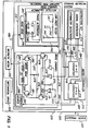
- FIG. 1 is a generalized schematic block diagram of data storage-retrieval system 200 coupled to external device 201 and including micro-controller 210, recording head circuitry 230, magnetic media 202, and mechanical drive 204.
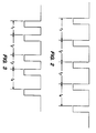
- FIG. 2 is a representative timing diagram of data signal 286 showing no asymmetry.
- FIG. 3 is a representative timing diagram of data signal 288 showing asymmetry.
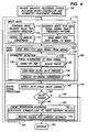
- FIG. 4 is an operational flow chart of data storage-retrieval system 200, including generally write mode 110, read mode 120, and digital signal processing 140 steps.
- FIG. 5 is a representative timing diagram showing asymmetric data signal 288 before and after phase adjustment by divide-by-two circuit 244.
- FIG. 6 is a representative timing diagram showing asymmetric data signal 288 with a deleted pulse 139.
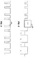
- FIG. 7 is a generalized schematic block diagram of write channel 234 showing circuitry in current source 260.
- FIG. 8 is a generalized schematic block diagram of alternative write channel 234' showing dual write current sources 285', 1285.
- FIG. 9 is a graphical chart illustrating asymmetry detector output change at phase reversal as a function of current ratio.
- FIG. 1 is a generalized block diagram of data storage-retrieval system 200 coupled to external device 201, which may store and retrieve electronic data in magnetic media 202 coupled to mechanical drive 204 in storage-retrieval system 200.
- Storage-retrieval system includes a processor or micro-controller 210 and recording head circuitry 230 for reading and writing signals to magnetic media 202, which may be a magnetic disk, drum, tape or the like.
- Micro-controller 210 may include a conventional digital microprocessor and associated memory for controlling recording operations of storage-retrieval system 200 according to the present invention.
- Micro-controller 210 memory includes instruction set 212 for signal generation 214 and asymmetry detection 216 as described herein.
- Micro-controller 210 may receive data signals from external device 201 and transmit or generate therefrom data signal 286 and control signals 284, 285 (and alternately control signal 1285) which are converted from digital to analog form 284', 285' by digital-to-analog converter 219, and received by write channel circuitry 234 through write head 250 in recording head circuitry 230 for writing or storing data signal 287 to certain storage locations in magnetic media 202.
- read channel circuitry 232 may retrieve or read from certain storage locations in magnetic media 202 data signal 288 to transmit or generate data signal 291, which is converted from analog to digital form 291' by analog-to-digital converter circuit 218, and thereby received by micro-controller 210 for transmission to external device 201.
- read channel circuitry 232 and write channel circuitry 234 are provided with read head 246 and write head 250 respectively for reading and writing data signals 288, 287 in magnetic media 202. It is contemplated that an integrated read-write head may serve the function of heads 246, 250.
- read channel circuitry 232 includes asymmetry detector 240 for detecting when read data signal 288 includes signal asymmetry.
- asymmetry detector 240 includes phase alternator 244 for receiving signal 288 as read by read head 246.
- phase alternator 244 includes a divide-by-two circuit, such as D-type flip-flop 248 as configured in FIG. 1.
- phase alternator 244 is coupled to low-pass filter 242, such as R-C circuit including resistors 241, 245 and capacitor 243 as configured in FIG. 1.
- Asymmetry detector 240 generates read, phase-reversed, and filtered data signal 291, which is received by A-D converter 218 in micro-controller 212 for generating digital-form signal 291'.
- write head 250 writes data signal 287 to magnetic media 202.
- write channel 234 receives from micro-controller 210 data signal 286 and control signals 284', 285'.
- control signal 284' is applied to current source 260, which is coupled to control write current applied to write head 250, preferably by controlling or balancing both, forward and backward, directions in write current passing through write head 250.
- control signal 285' is received by amplifier circuitry including resistors 273, 275 and operational amplifier 274 as configured in FIG. 1. Such amplifier circuitry then generates drive signal 292, which is applied to transistors 276, 293, as configured in FIG. 1.
- data signal 286 is received from micro-controller 210, and data signal 286 is then buffered 271 and inverted 272 to be applied respectively, as configured in FIG. 1, to bases of transistors 293, 276.
- transistors 276, 293 and resistors 277, 279, which are coupled to power, are coupled separately to bases of transistors 282, 281 respectively, as configured in FIG. 1.
- power is coupled through resistor 278 to transistors 282, 281, as configured in FIG. 1. As thus configured, transistors 281, 282 are coupled to drive current in write head 250.
- FIG. 7 a more detailed schematic of write channel circuitry 234 is shown to illustrate representative circuitry within current source 260.
- current source 260 receives control signal 284' to generate control signal 289 coupled to write head 250.
- current source 260 includes operational amplifier 266 coupled to resistors 261-266.
- signal 285' functions as a write-balance current
- signal 284' functions as an asymmetry control signal.
- FIG. 8 an alternate embodiment of write channel circuitry 234' is shown.
- dual write control currents 285', 1285 are generated, preferably according to newly-calculated current balance values from linear regression analysis 150 in digital signal processing mode 140 from signal generation instructions 214 in micro-controller 210 to be applied respectively to transistors 293, 276 as configured in FIG. 8.
- transistors 276, 293 are uncoupled from each other, such that signals 285', 1285 may balance write current applied to write head 250.
- write balance signal 285' is applied to resistor 273 coupled to operational amplifier 274 and resistor 275; and write balance signal 1285 is applied similarly to resistor 1273 coupled to operational amplifier 1274 and resistor 1275.
- a representative timing diagram shows data signal 286 generated by signal generation instructions 214 in micro-controller 210.
- data signal 286, which is written to magnetic media 202 includes equally-spaced signal pulses, such that the duty cycle of signal 286 is necessarily 50% when generated initially.
- a representative timing diagram shows read data signal 288, which may be read by read head 246 from magnetic media 202, embodying signal asymmetry whereby signal pulse widths are not equal (i.e., asymmetrical) with each other.
- FIG. 4 a generalized flow chart shows the operation of a system such as storage-retrieval system 200 of FIG. 1.
- a magnetic recording system is provided 100, including micro-controller and asymmetry adjustment firmware.
- the provided system operates in write mode 110, read mode 120, and digital signal processing mode 140.
- micro-controller 210 causes write channel circuitry 234 to generate 112, preferably according to signal generation instructions 214, a write-balance value for forward and backward write-current direction (i.e., in write head 250) in accordance with calculations performed by micro-controller 210 during digital signal processing mode 140.
- the generated value is processed 114 by D-A converter circuit 219 to produce control signals 284', 285' which are applicable to control or balance write current 289 in write head 250.
- micro-controller 210 generates, preferably according to signal generation instructions 214, write test data signal 286 having a single-frequency pattern and a 50% duty cycle, as shown in FIG. 2. In accordance with the present invention, such signal 286 is written 118 to magnetic media 202 by write head 250.
- micro-controller 210 causes read channel circuitry 232 to read 122 test data signal from magnetic media, through read head 246.
- the read signal is received from read head 246 by asymmetry detector 240 for asymmetry detection 130 of the read signal, preferably according to asymmetry detection instructions 216 executed by micro-controller 210.
- the read signal is phase-reversed or alternated 132, preferably by passing the read signal through divide-by-two circuit 248, and preferably deleting a pulse 139 from the read signal pulse train.
- the read signal is phase-reversed or alternated 132, preferably by passing the read signal through divide-by-two circuit 248, and preferably deleting a pulse 139 from the read signal pulse train.
- at least one phase reversal occurs during read-signal asymmetry detection and digital signal processing 140, as described herein.
- FIG. 5 a representative timing diagram shows phase alternator 244 performing a divide-by-two function on an incoming data signal from read head 246.
- pulse deletion 139 is illustrated, whereby such pulse deletion mathematically has the equivalent effect of phase reversal (i.e., of duty cycle.)
- phase-reversed signal is filtered 134 through R-C, low-pass filter 242 to provide a steady-state value or signal magnitude (i.e., having a value of 100*T d *(V h +V l ) , where T d is the duty cycle, and V h and V l respectively are logic high and low of the processed signal,) thereby indicating signal asymmetry.
- the value is then passed through 136 A-D converter 218 to convert its form for digital signal processing 140.
- phase reversal and magnitude generation serves to allow micro-controller 210 to identify electronically and automatically the presence of signal asymmetry in the read signal, i.e., by detecting a value which is representative of duty cycle variation from 50%, when no signal asymmetry is assumed to exist in the read signal.
- asymmetry detection is possible because, duty cycle varies as a function of read-signal asymmetry, and the output of phase alternator circuit 244 is similarly a function of such asymmetry.
- micro-controller 210 evaluates or monitors the indicated value to detect 142 a change in duty cycle between a pre-recording duty cycle of generated signal 286 and a post-recording duty cycle of processed signal 291.
- a linear-regression analysis 150 is performed by micro-controller 210 to provide 156 a write-current balance value, preferably provided over a relatively wide value range, such that asymmetry detection is facilitated by off-balancing about a write signal symmetry or current balance point.
- micro-controller 210 calculates 152 a straight line fit of prior, recorded balance values to adjust a newly-generated, modified balance value, thereby electronically varying signal asymmetry.
- Each generated value in recorded 154 according to its corresponding write current setting.
- Such generated values are applicable by signal generation instructions 214 to apply for asymmetry correction control signals 284, 285 (and, in alternate embodiment shown in FIG. 8, control signal 1285, once converted by D-A converter 219 to analog form.)
- micro-controller 210 may repeat 156 for successive asymmetry correction trials write mode 110, read mode 120, and digital signal processing 140 to generate or adjust a new current balance value.
- storage-retrieval system 200 serves as a servo-mechanism having signal feedback to compensate or balance for subsequently-detected magnetic recording degradation which may contribute to signal asymmetry.
- FIG. 9 a graphical chart illustrates the functional relationship between a representative current ratio and asymmetry detector output change at phase reversal, in accordance with the present invention.
- V vertex
- micro-controller 210 mathematically calculates or employs straight line fitting or linear regression 150 of previously-generated values to achieve graphically such zero output change, thereby finding a so-called "zero” or "null" point.
Landscapes
- Engineering & Computer Science (AREA)
- Signal Processing (AREA)
- Digital Magnetic Recording (AREA)
- Signal Processing For Digital Recording And Reproducing (AREA)
Applications Claiming Priority (2)
| Application Number | Priority Date | Filing Date | Title |
|---|---|---|---|
| US08/067,312 US5485320A (en) | 1993-05-24 | 1993-05-24 | Method and apparatus for adjusting asymmetric recording signals |
| US67312 | 1993-05-24 |
Publications (2)
| Publication Number | Publication Date |
|---|---|
| EP0651373A2 true EP0651373A2 (fr) | 1995-05-03 |
| EP0651373A3 EP0651373A3 (fr) | 1995-10-18 |
Family
ID=22075143
Family Applications (1)
| Application Number | Title | Priority Date | Filing Date |
|---|---|---|---|
| EP94107988A Withdrawn EP0651373A3 (fr) | 1993-05-24 | 1994-05-24 | Méthode et appareil pour ajustement de signaux asymétriques d'enregistrement. |
Country Status (5)
| Country | Link |
|---|---|
| US (1) | US5485320A (fr) |
| EP (1) | EP0651373A3 (fr) |
| JP (1) | JPH07147002A (fr) |
| CN (1) | CN1103197A (fr) |
| TW (1) | TW228634B (fr) |
Cited By (2)
| Publication number | Priority date | Publication date | Assignee | Title |
|---|---|---|---|---|
| EP0959470A1 (fr) * | 1998-05-19 | 1999-11-24 | Hewlett-Packard Company | Calibrage d'égalisation d'ecriture dans un dispositif de stockage de données |
| EP0965989A1 (fr) * | 1998-05-19 | 1999-12-22 | Hewlett-Packard Company | Calibrage de compensation d'écriture dans un dispositif de stockage des données |
Families Citing this family (6)
| Publication number | Priority date | Publication date | Assignee | Title |
|---|---|---|---|---|
| JP3190194B2 (ja) * | 1993-08-19 | 2001-07-23 | 三菱電機株式会社 | 磁気記録方法および装置 |
| US5787005A (en) * | 1995-10-02 | 1998-07-28 | Aiwa Co., Ltd. | Method and apparatus for signal threshold adjustment that compensates for signal asymmetry |
| KR0166157B1 (ko) * | 1995-12-27 | 1999-03-20 | 김광호 | 자기 기록장치의 기록전류 제어회로 및 방법 |
| US6108484A (en) * | 1996-05-31 | 2000-08-22 | Lg Electronics Inc. | Self-diagnosing apparatus and method for video recording and reproducing apparatus |
| US7411754B2 (en) * | 2006-08-08 | 2008-08-12 | Hitachi Global Storage Technologies Netherlands B.V. | System and method for measuring readback signal amplitude asymmetry in a perpendicular magnetic recording disk drive |
| US9153248B1 (en) | 2015-02-25 | 2015-10-06 | HGST Netherlands B.V. | Hard disk drive preamplifier with write driver having bypass current sources for compensation of write head magnetic asymmetry |
Family Cites Families (16)
| Publication number | Priority date | Publication date | Assignee | Title |
|---|---|---|---|---|
| JPS57100613A (en) * | 1980-12-12 | 1982-06-22 | Shiro Okamura | Magnetic recording and reproducing system |
| JPS583118A (ja) * | 1981-06-30 | 1983-01-08 | Sony Corp | デイスク再生装置の波形変換回路 |
| JPS5862805A (ja) * | 1981-10-09 | 1983-04-14 | Nippon Gakki Seizo Kk | テ−プレコ−ダにおける自動録音レベル設定装置 |
| JPS58199410A (ja) * | 1982-05-14 | 1983-11-19 | Hitachi Denshi Ltd | デイジタル信号の磁気記録方法 |
| JPS59110017A (ja) * | 1982-12-13 | 1984-06-25 | Hitachi Ltd | 磁気記録方式 |
| JPS61123067A (ja) * | 1984-11-20 | 1986-06-10 | Fujitsu Ltd | 磁気テ−プ装置の試験方法 |
| US4669013A (en) * | 1985-04-02 | 1987-05-26 | International Business Machines Corporation | Multiple coils for reduction of stray magnetic fields in disk file actuators |
| US4811127A (en) * | 1986-10-22 | 1989-03-07 | Victor Company Of Japan, Ltd. | Magnetic recording and reproducing apparatus |
| JP2647875B2 (ja) * | 1987-12-25 | 1997-08-27 | 株式会社日立製作所 | 光磁気信号記録再生方法 |
| JPH03295015A (ja) * | 1990-04-13 | 1991-12-26 | Onkyo Corp | アジマスずれ検出装置 |
| US5204788A (en) * | 1990-06-15 | 1993-04-20 | Mitsubishi Denki Kabushiki Kaisha | Digital magnetic recording and reproducing circuit for suppressing generation of asymmetry |
| US5333084A (en) * | 1990-07-13 | 1994-07-26 | Gregory M. Galloway | Electronically alignable flexible disk drive |
| US5185681A (en) * | 1990-09-28 | 1993-02-09 | Seagate | Thermal offset compensation for high density disk drives |
| US5262904A (en) * | 1991-01-22 | 1993-11-16 | International Business Machines Corporation | Method and apparatus for measuring and compensating nonlinear bitshift |
| US5278702A (en) * | 1991-04-12 | 1994-01-11 | Western Digital Corporation | Data synchronizer with symmetric window generation |
| US5357520A (en) * | 1992-01-31 | 1994-10-18 | International Business Machines Corporation | Method and apparatus for precompensation value determination in a PRML data channel |
-
1993
- 1993-05-24 US US08/067,312 patent/US5485320A/en not_active Expired - Fee Related
- 1993-06-11 TW TW082104248A patent/TW228634B/zh active
-
1994
- 1994-05-24 CN CN94105869.7A patent/CN1103197A/zh active Pending
- 1994-05-24 EP EP94107988A patent/EP0651373A3/fr not_active Withdrawn
- 1994-05-24 JP JP6132431A patent/JPH07147002A/ja active Pending
Cited By (3)
| Publication number | Priority date | Publication date | Assignee | Title |
|---|---|---|---|---|
| EP0959470A1 (fr) * | 1998-05-19 | 1999-11-24 | Hewlett-Packard Company | Calibrage d'égalisation d'ecriture dans un dispositif de stockage de données |
| EP0965989A1 (fr) * | 1998-05-19 | 1999-12-22 | Hewlett-Packard Company | Calibrage de compensation d'écriture dans un dispositif de stockage des données |
| US6256158B1 (en) | 1998-05-19 | 2001-07-03 | Hewlett-Packard Company | Calibrating write pre-equalization in a data storage device |
Also Published As
| Publication number | Publication date |
|---|---|
| JPH07147002A (ja) | 1995-06-06 |
| EP0651373A3 (fr) | 1995-10-18 |
| US5485320A (en) | 1996-01-16 |
| CN1103197A (zh) | 1995-05-31 |
| TW228634B (en) | 1994-08-21 |
Similar Documents
| Publication | Publication Date | Title |
|---|---|---|
| US5623474A (en) | Disk apparatus having automatic adjustment of adaptive filter equalization parameter using training pattern | |
| JP2648554B2 (ja) | Prmlディスク駆動システムの非同期ゲイン調整方法および装置 | |
| DE3650466T2 (de) | Wiedergabegerät für optische Platten | |
| US5461517A (en) | Magneto-resistance effect type of recording/reproducing head | |
| US5677801A (en) | Magnetic recording/reproducing apparatus for automatically adjusting a recording current in accordance with the wear of a read head | |
| US4085427A (en) | Transducer positioning system | |
| JPH0443349B2 (fr) | ||
| EP0651373A2 (fr) | Méthode et appareil pour ajustement de signaux asymétriques d'enregistrement | |
| JPH0241801B2 (fr) | ||
| US4651235A (en) | Magnetic data transfer apparatus having a combined read/write head | |
| GB1120752A (en) | Phase and frequency correction system | |
| US5467231A (en) | Using recorded data for auto calibration of fixed gain of a read amplifier in a data storage device | |
| DE3851526T2 (de) | Digitales bandaufnahmegerät. | |
| JPS58199410A (ja) | デイジタル信号の磁気記録方法 | |
| JPH0713090Y2 (ja) | データレコーダ | |
| US5418656A (en) | Drop-out detecting circuit | |
| US6469851B1 (en) | Acquisition signal error estimator | |
| JPH06231410A (ja) | 磁気ディスク装置 | |
| JP2584821B2 (ja) | 光ディスク再生装置 | |
| KR0133866Y1 (ko) | 드롭 아웃 펄스를 이용한 테이프 재생 속도 검출 회로 | |
| JPH01165004A (ja) | 磁気記録再生装置の再生回路 | |
| JPH0676216A (ja) | イコライザ制御による信号検出方式およびそれを用いた磁気記録装置 | |
| EP0901125A1 (fr) | Récupération d'horloge pour un système de stockage de données sur bande | |
| JPS59162607A (ja) | 磁気記憶装置 | |
| JPH052710A (ja) | 磁気記録再生装置のデータ再生装置 |
Legal Events
| Date | Code | Title | Description |
|---|---|---|---|
| PUAI | Public reference made under article 153(3) epc to a published international application that has entered the european phase |
Free format text: ORIGINAL CODE: 0009012 |
|
| AK | Designated contracting states |
Kind code of ref document: A2 Designated state(s): DE FR GB IE |
|
| PUAL | Search report despatched |
Free format text: ORIGINAL CODE: 0009013 |
|
| AK | Designated contracting states |
Kind code of ref document: A3 Designated state(s): DE FR GB IE |
|
| 17P | Request for examination filed |
Effective date: 19960221 |
|
| STAA | Information on the status of an ep patent application or granted ep patent |
Free format text: STATUS: THE APPLICATION HAS BEEN WITHDRAWN |
|
| 18W | Application withdrawn |
Withdrawal date: 19970107 |