EP0651376A1 - Patin de vol à plots de soudures composites et procédé de réalisation - Google Patents
Patin de vol à plots de soudures composites et procédé de réalisation Download PDFInfo
- Publication number
- EP0651376A1 EP0651376A1 EP94402425A EP94402425A EP0651376A1 EP 0651376 A1 EP0651376 A1 EP 0651376A1 EP 94402425 A EP94402425 A EP 94402425A EP 94402425 A EP94402425 A EP 94402425A EP 0651376 A1 EP0651376 A1 EP 0651376A1
- Authority
- EP
- European Patent Office
- Prior art keywords
- flight
- pads
- pad
- bases
- deposited
- Prior art date
- Legal status (The legal status is an assumption and is not a legal conclusion. Google has not performed a legal analysis and makes no representation as to the accuracy of the status listed.)
- Granted
Links
- 229910000679 solder Inorganic materials 0.000 title claims description 13
- 238000000034 method Methods 0.000 title claims description 11
- 238000004519 manufacturing process Methods 0.000 title claims description 5
- 239000002131 composite material Substances 0.000 title description 4
- 239000000463 material Substances 0.000 claims description 25
- 238000002844 melting Methods 0.000 claims description 11
- 230000008018 melting Effects 0.000 claims description 11
- RYGMFSIKBFXOCR-UHFFFAOYSA-N Copper Chemical compound [Cu] RYGMFSIKBFXOCR-UHFFFAOYSA-N 0.000 claims description 4
- PXHVJJICTQNCMI-UHFFFAOYSA-N Nickel Chemical compound [Ni] PXHVJJICTQNCMI-UHFFFAOYSA-N 0.000 claims description 4
- ATJFFYVFTNAWJD-UHFFFAOYSA-N Tin Chemical compound [Sn] ATJFFYVFTNAWJD-UHFFFAOYSA-N 0.000 claims description 4
- 239000004020 conductor Substances 0.000 claims description 4
- 229910052802 copper Inorganic materials 0.000 claims description 4
- 239000010949 copper Substances 0.000 claims description 4
- 239000000758 substrate Substances 0.000 claims description 3
- 229910000990 Ni alloy Inorganic materials 0.000 claims description 2
- 229910045601 alloy Inorganic materials 0.000 claims description 2
- 239000000956 alloy Substances 0.000 claims description 2
- 229910052738 indium Inorganic materials 0.000 claims description 2
- APFVFJFRJDLVQX-UHFFFAOYSA-N indium atom Chemical compound [In] APFVFJFRJDLVQX-UHFFFAOYSA-N 0.000 claims description 2
- 229910052759 nickel Inorganic materials 0.000 claims description 2
- 230000004927 fusion Effects 0.000 description 4
- LQBJWKCYZGMFEV-UHFFFAOYSA-N lead tin Chemical compound [Sn].[Pb] LQBJWKCYZGMFEV-UHFFFAOYSA-N 0.000 description 4
- 238000003466 welding Methods 0.000 description 4
- NJPPVKZQTLUDBO-UHFFFAOYSA-N novaluron Chemical compound C1=C(Cl)C(OC(F)(F)C(OC(F)(F)F)F)=CC=C1NC(=O)NC(=O)C1=C(F)C=CC=C1F NJPPVKZQTLUDBO-UHFFFAOYSA-N 0.000 description 2
- VYZAMTAEIAYCRO-UHFFFAOYSA-N Chromium Chemical compound [Cr] VYZAMTAEIAYCRO-UHFFFAOYSA-N 0.000 description 1
- XUIMIQQOPSSXEZ-UHFFFAOYSA-N Silicon Chemical compound [Si] XUIMIQQOPSSXEZ-UHFFFAOYSA-N 0.000 description 1
- 240000008042 Zea mays Species 0.000 description 1
- 229910052804 chromium Inorganic materials 0.000 description 1
- 239000011651 chromium Substances 0.000 description 1
- 238000010276 construction Methods 0.000 description 1
- 230000007547 defect Effects 0.000 description 1
- 238000005530 etching Methods 0.000 description 1
- 238000010438 heat treatment Methods 0.000 description 1
- 229910052751 metal Inorganic materials 0.000 description 1
- 239000002184 metal Substances 0.000 description 1
- 230000003287 optical effect Effects 0.000 description 1
- 238000000206 photolithography Methods 0.000 description 1
- 238000005498 polishing Methods 0.000 description 1
- 229910052710 silicon Inorganic materials 0.000 description 1
- 239000010703 silicon Substances 0.000 description 1
Images


Classifications
-
- G—PHYSICS
- G11—INFORMATION STORAGE
- G11B—INFORMATION STORAGE BASED ON RELATIVE MOVEMENT BETWEEN RECORD CARRIER AND TRANSDUCER
- G11B5/00—Recording by magnetisation or demagnetisation of a record carrier; Reproducing by magnetic means; Record carriers therefor
- G11B5/48—Disposition or mounting of heads or head supports relative to record carriers ; arrangements of heads, e.g. for scanning the record carrier to increase the relative speed
- G11B5/4806—Disposition or mounting of heads or head supports relative to record carriers ; arrangements of heads, e.g. for scanning the record carrier to increase the relative speed specially adapted for disk drive assemblies, e.g. assembly prior to operation, hard or flexible disk drives
- G11B5/4853—Constructional details of the electrical connection between head and arm
-
- G—PHYSICS
- G11—INFORMATION STORAGE
- G11B—INFORMATION STORAGE BASED ON RELATIVE MOVEMENT BETWEEN RECORD CARRIER AND TRANSDUCER
- G11B21/00—Head arrangements not specific to the method of recording or reproducing
- G11B21/16—Supporting the heads; Supporting the sockets for plug-in heads
- G11B21/20—Supporting the heads; Supporting the sockets for plug-in heads while the head is in operative position but stationary or permitting minor movements to follow irregularities in surface of record carrier
- G11B21/21—Supporting the heads; Supporting the sockets for plug-in heads while the head is in operative position but stationary or permitting minor movements to follow irregularities in surface of record carrier with provision for maintaining desired spacing of head from record carrier, e.g. fluid-dynamic spacing, slider
-
- Y—GENERAL TAGGING OF NEW TECHNOLOGICAL DEVELOPMENTS; GENERAL TAGGING OF CROSS-SECTIONAL TECHNOLOGIES SPANNING OVER SEVERAL SECTIONS OF THE IPC; TECHNICAL SUBJECTS COVERED BY FORMER USPC CROSS-REFERENCE ART COLLECTIONS [XRACs] AND DIGESTS
- Y10—TECHNICAL SUBJECTS COVERED BY FORMER USPC
- Y10T—TECHNICAL SUBJECTS COVERED BY FORMER US CLASSIFICATION
- Y10T29/00—Metal working
- Y10T29/49—Method of mechanical manufacture
- Y10T29/49002—Electrical device making
- Y10T29/4902—Electromagnet, transformer or inductor
- Y10T29/49021—Magnetic recording reproducing transducer [e.g., tape head, core, etc.]
- Y10T29/49027—Mounting preformed head/core onto other structure
- Y10T29/4903—Mounting preformed head/core onto other structure with bonding
Definitions
- the subject of the present invention is a flight pad with composite solder pads and a method of making it. It finds an application in magnetic recording, in particular in recording on hard disk.
- Flight pads with magnetic heads are generally glued to the end of an arm serving as a spring.
- the electrical connections between the head and the external circuits are ensured by twisted conducting wires welded on the shoe and supported by the arm.
- connection tracks made on the upper face of the pad that is to say the face opposite to the disc
- connection tracks made on the upper face of the pad that is to say the face opposite to the disc
- solder pads are produced between the tracks of the pad and those of the arm.
- the object of the present invention is precisely to avoid this drawback.
- each solder pad is composite, in the sense that it comprises two parts, a first part, or base, which is made of a material which is not fusible at the temperature at which welding is carried out, this base having a certain controlled height which will ensure a minimum spacing between the shoe and the arm, and a second part, which is a stud made of fusible material, which will carry out the actual welding.
- first part or base
- second part which is a stud made of fusible material
- the present invention relates to a flight pad comprising solder pads for assembly with a spring arm, characterized in that each solder pad comprises, on the one hand, a base secured to the pad flight, this base having a controlled height and being made of a first material and, on the other hand, a fuse block disposed on the base, this fuse block being made of a second material having a lower melting temperature than that of the first.
- the first material is advantageously a conductive material such as copper, nickel or nickel alloys for example.
- the second material can be for example tin, lead, indium or their alloys (for example, tin-lead).
- the studs can be used both for the mechanical strength of the assembly and for electrical connections. But possibly, some studs can only be used for mechanical strength.
- the base will be produced on a connection track formed on the flight pad and the fuse pad will be in contact with a similar connection track, arranged under the spring arm.
- third additional fuse pads are also deposited on the end of the spring arm, these additional pads being made of the second material and being arranged at locations which correspond to the fuse pads deposited on the bases , these third additional studs coming to be welded on the first during the last operation.
- solder pads on the skate itself is particularly advantageous in the case of collective skate constructions.
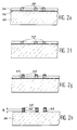
- FIGS 2a to 2h illustrate eight steps of an embodiment method according to the invention.
- a substrate 30 for example a silicon wafer, which will be used to make the flight pad (FIG. 2a).
- a thin conductive layer 32 having good adhesion is deposited, for example a layer of chromium (FIG. 2b).
- a photosensitive film 34 having a thickness h equal to the minimum desired distance between the flight pad and the end of the spring arm (Fig. 2c). This thickness can be, for example, 75 ⁇ m.
- openings 36 are formed at suitable locations, with a diameter equal to the diameter of the bases that one wishes to make (FIG. 2d). This diameter can vary between around 100 and 200 ⁇ m.
- Conductive pads 38 are formed in these openings by electrolytic growth of a first conductive material, for example copper, taking the conductive layer 32 as the electrode (FIG. 2e).
- a first conductive material for example copper
- the studs obtained are planarized, by a polishing method for example, to bring the metal back to the level of the sheet 34.
- the bases 40 are thus obtained (fig. 2f).
- the fuse pads 42 are formed by electrolytic growth of a second material such as tin-lead on the bases 40 (FIG. 2g).
- the sheet 34 is then dissolved and the adhesion layer 32 is etched.
- the composite pads 40-42 remain (fig. 2h).
- pads are deposited 40-42 on a flight pad 58 but also additional fuse pads 44 under the spring arm 56.
- These pads 44 may be made of the same material as the fuse pads 42, for example tin-lead.
- These additional pads are arranged opposite the fuse pads 42 arranged at the top of the bases 40 on the flight pad.
- the flight pad is assembled under the end of the spring arm preferably in accordance with FIG. 4.
- the shoe 58 is held on a reference plane 60, by suction for example.
- the spring arm 56 is held on a pedestal 62 secured to the reference plane 60.
- This pedestal 62 represents the foot of the spring arm in the final assembly. The arm is therefore placed in the same position that it will occupy in operation.
- the relative positioning of the pad relative to the spring arm is carried out either manually, under a microscope, or automatically, by optical recognition.
- the arm exerts a force on the solder pads 40, 42.
- the temperature of the solder pads is raised above the melting temperature of the pads 42 (and, where appropriate, the pads 44).
- the temperature is brought in the range 150-250 ° C.
- the fuse pads melt and crash more or less depending on the position and dimensions of the different parts.
- the minimum space between the spring and the shoe will be equal to the thickness of the copper studs 40, the thickness of the tin including the differences in height due to the incorrect torsion of the spring.
- the spring will have kept its shape in a slight bias, but the plane of the pad will be perfectly parallel to that of the foot of the spring.
Landscapes
- Supporting Of Heads In Record-Carrier Devices (AREA)
- Manufacturing Of Electrical Connectors (AREA)
- Manufacture Of Switches (AREA)
Abstract
Description
- La présente invention a pour objet un patin de vol à plots de soudure composites et un procédé de réalisation. Elle trouve une application dans l'enregistrement magnétique, notamment dans l'enregistrement sur disque dur.
- Les patins de vol à tête magnétique sont en général collés à l'extrémité d'un bras faisant office de ressort. Les connexions électriques entre la tête et les circuits extérieurs sont assurées par des fils conducteurs torsadés soudés sur le patin et supportés par le bras.
- Pour éviter l'emploi de tels fils, on peut avoir recours à des pistes de connexion réalisées sur la face supérieure du patin (c'est-à-dire la face opposée au disque) et sur le bras-ressort. Pour réaliser les connexions électriques, tout en assurant le soudage et la tenue mécanique du patin sous l'extrémité du bras, on réalise des plots de soudure entre les pistes du patin et celles du bras.
- Le document US-A-4,789,914 décrit ainsi un assemblage qui est représenté sur la figure 1 annexée. Sur cette figure, on voit un patin de vol 10 avec des pistes de connexion 12, l'extrémité 20 d'un bras-ressort, avec un circuit de connexion 22 et, entre les deux, des plots de soudure 24.
- Ce moyen de fixation du patin sous le bras présente l'inconvénient de ne pas assurer un écartement contrôlé entre le bras et le patin. En effet, sous la pression exercée par le bras-ressort, certains plots s'écrasent lors de l'opération de soudure et le patin peut venir en contact avec le bras. Sa mobilité s'en trouve entravée.
- La présente invention a justement pour but d'éviter cet inconvénient.
- A cette fin, l'invention prévoit que chaque plot de soudure est composite, en ce sens qu'il comprend deux parties, une première partie, ou embase, qui est réalisée en un matériau qui n'est pas fusible à la température à laquelle on procède au soudage, cette embase ayant une certaine hauteur contrôlée qui va assurer un écartement minimum entre le patin et le bras, et une seconde partie, qui est un plot en matériau fusible, lequel va réaliser la soudure proprement dite. Ainsi, même si les plots fusibles s'écrasent plus ou moins selon les défauts de planérité des pièces, le patin et le bras seront toujours écartés au minimum d'une distance égale à la hauteur des embases.
- De façon précise, la présente invention a pour objet un patin de vol comprenant des plots de soudure pour un assemblage avec un bras-ressort, caractérisé par le fait que chaque plot de soudure comprend, d'une part, une embase solidaire du patin de vol, cette embase ayant une hauteur contrôlée et étant réalisée en un premier matériau et, d'autre part, un plot fusible disposé sur l'embase, ce plot fusible étant réalisé en un second matériau ayant une température de fusion plus basse que celle du premier.
- Le premier matériau est avantageusement un matériau conducteur comme le cuivre, le nickel ou les alliages de nickel par exemple.
- Le second matériau peut être par exemple l'étain, le plomb, l'indium ou leurs alliages (par exemple, l'étain-plomb).
- Dans un assemblage conforme à l'invention, les plots peuvent servir à la fois à la tenue mécanique de l'ensemble et à des connexions électriques. Mais éventuellement, certains plots peuvent ne servir qu'à la tenue mécanique.
- Pour ceux des plots qui servent de connexion électrique, l'embase sera réalisée sur une piste de connexion formée sur le patin de vol et le plot fusible sera en contact avec une piste de connexion similaire, disposée sous le bras-ressort.
- La présente invention a également pour objet un procédé de réalisation d'un assemblage patin de vol/bras-ressort, le patin étant conforme à ce qui vient d'être défini. Selon l'invention, ce procédé comprend les opérations suivantes :
- on réalise sur un patin de vol des embases en un premier matériau ayant une première température de fusion, ces embases ayant une hauteur contrôlée,
- on forme ensuite, sur chacune de ces embases, un second plot fusible en un second matériau ayant une seconde température de fusion inférieure à celle du premier matériau,
- on assemble le bras-ressort sur le patin de vol dans une position qui sera celle de la position de travail de l'assemblage,
- on élève la température des plots au-dessus de la seconde température de fusion du second matériau mais en dessous de la première température de fusion du premier.
- Dans un mode particulier de mise en oeuvre, on dépose en outre des troisièmes plots fusibles supplémentaires sur l'extrémité du bras ressort, ces plots supplémentaires étant réalisés dans le second matériau et étant disposés à des emplacements qui corespondent aux plots fusibles déposés sur les embases, ces troisièmes plots supplémentaires venant se souder sur les premiers lors de la dernière opération.
- La réalisation des plots de soudure sur le patin lui-même est particulièrement intéressante dans le cas des réalisations collectives de patins.
-
- la figure 1, déjà décrite, montre un assemblage selon l'art antérieur,
- les figures 2a à 2h montrent diverses étapes d'un procédé selon l'invention,
- la figure 3 illustre une variante où les plots fusibles sont disposés à la fois sous le bras-ressort et sur le patin,
- la figure 4 illustre schématiquement le mode de montage du patin sous le bras-ressort.
- Les figures 2a à 2h illustrent huit étapes d'un procédé de réalisation conforme à l'invention.
- On part d'un substrat 30, par exemple une plaquette de silicium, qui va servir à réaliser le patin de vol (fig. 2a).
- Sur ce substrat 30, on dépose une couche mince conductrice 32 ayant une bonne adhérence, par exemple une couche de chrome (fig. 2b).
- On dépose ensuite, sur cette couche conductrice 32, un film photosensible 34 ayant une épaisseur h égale à l'intervalle minimum souhaité entre le patin de vol et l'extrémité du bras-ressort (Fig. 2c) . Cette épaisseur peut être par exemple de 75 µm.
- Par photolithographie de ce film 34, on forme des ouvertures 36 à des emplacements appropriés, avec un diamètre égal au diamètre des embases que l'on veut réaliser (fig. 2d). Ce diamètre peut varier entre environ 100 et 200 µm.
- On forme des plots conducteurs 38 dans ces ouvertures par croissance électrolytique d'un premier matériau conducteur, par exemple du cuivre, en prenant la couche conductrice 32 comme électrode (fig. 2e).
- On planarise les plots obtenus, par une méthode de polissage par exemple, pour ramener le métal au niveau de la feuille 34. On obtient ainsi les embases 40 (fig. 2f).
- On forme les plots fusibles 42 par croissance électrolytique d'un second matériau comme l'étain-plomb sur les embases 40 (fig. 2g).
- On dissout ensuite la feuille 34 et on grave la couche d'adhérence 32. Il reste les plots composites 40-42 (fig. 2h).
- Le procédé qui vient d'être décrit suppose que les plots sont réalisés par croissance électrolytique. On pourrait procéder autrement (par exemple par gravure), auquel cas la couche conductrice d'adhérence 32 ne serait pas nécessaire.
- Dans un mode de mise en oeuvre possible illustré sur la figure 3, on dépose non seulement des plots 40-42 sur un patin de vol 58 mais également des plots fusibles supplémentaires 44 sous le bras-ressort 56. Ces plots 44 peuvent être dans le même matériau que les plots fusibles 42, par exemple de l'étain-plomb. Ces plots supplémentaires sont disposés en regard des plots fusibles 42 disposés au sommet des embases 40 sur le patin de vol.
- L'assemblage du patin de vol sous l'extrémité du bras-ressort s'effectue de préférence conformément à la figure 4.
- Le patin 58 est tenu sur un plan de référence 60, par aspiration par exemple. Le bras-ressort 56 est tenu sur un piédestal 62 solidaire du plan de référence 60.
- Ce piédestal 62 représente le pied du bras-ressort dans le montage définitif. Le bras est donc placé dans la position même qu'il occupera en fonctionnement.
- Le positionnement relatif du patin par rapport au bras-ressort s'effectue soit manuellement, sous microscope, soit automatiquement, par reconnaissance optique.
- Dans cette position, le bras exerce un effort sur les plots de soudure 40, 42.
- A l'aide d'un faisceau laser, ou de moyens de chauffage infrarouge, ou de tout autre moyen, on élève la température des plots de soudure au-dessus de la température de fusion des plots 42 (et, le cas échéant des plots supplémentaires 44).
- En pratique, avec les matériaux habituellement utilisés (étain, étain-plomb), la température est portée dans la plage 150-250°C. Les plots fusibles fondent et s'écrasent plus ou moins selon la position et les dimensions des différentes pièces.
- Ainsi, même si le bras-ressort n'est pas parfaitement parallèle au plan du patin (ce qui arrive fréquemment), l'espace minimum entre le ressort et le patin sera égal à l'épaisseur des plots de cuivre 40, l'épaisseur d'étain comprenant les différences de hauteurs dues à la mauvaise torsion du ressort. Ainsi, quand l'ensemble sera monté sur le disque d'enregistrement, le ressort aura gardé sa forme en léger biais, mais le plan du patin, lui, sera parfaitement parallèle à celui du pied du ressort.
Claims (10)
- Patin de vol comprenant des plots de soudure (24, 40, 42, 44) pour un assemblage avec un bras-ressort, caractérisé par le fait que chaque plot de soudure comprend, d'une part, une embase (40) solidaire du patin de vol (10, 58), cette embase ayant une hauteur contrôlée (h) et étant réalisée en un premier matériau et, d'autre part, un plot fusible (42) disposé sur l'embase (40), ce plot fusible (42) étant réalisé en un second matériau ayant une température de fusion plus basse que celle du premier.
- Patin de vol selon la revendication 1, caractérisé par le fait que le premier matériau est un matériau conducteur.
- Patin de vol selon la revendication 2, caractérisé par le fait que le matériau conducteur est pris dans le groupe constitué par le cuivre, le nickel et les alliages de nickel.
- Patin de vol selon la revendication 1, caractérisé par le fait que le second matériau est pris dans le groupe constitué par l'étain, le plomb, l'indium et leurs alliages.
- Patin de vol selon la revendication 1, caractérisé par le fait que pour l'un au moins des plots de soudure, l'embase (40) est en contact avec une connexion électrique disposée sur le patin de vol (58).
- Procédé de réalisation d'un assemblage patin de vol/bras-ressort, le patin étant conforme à la revendication 1, caractérisé par le fait qu'il comprend les opérations suivantes :- on réalise, sur un patin de vol (58) des embases (40) en un premier matériau ayant une première température de fusion, ces embases ayant une hauteur contrôlée (h),- on forme ensuite, sur chacune de ces embases (40), un plot fusible (42) en un second matériau ayant une seconde température de fusion inférieure à celle du premier matériau,- on assemble le bras-ressort (56) sur le patin de vol (58) dans une position qui sera celle de la position de travail de l'assemblage,- on élève la température des plots (40, 42) au-dessus de la température de fusion du second matériau mais en dessous de la température de fusion du premier.
- Procédé selon la revendication 6, caractérisé par le fait qu'on dépose en outre des plots fusibles supplémentaires (44) sur l'extrémité du bras ressort (56), ces plots supplémentaires (44) étant réalisés dans le second matériau et étant disposés à des emplacements qui correspondent aux plots fusibles (42) déposés sur les embases (40), ces plots supplémentaires (44) venant se souder sur les premiers (42) lors de la dernière opération.
- Procédé selon la revendication 6, caractérisé par le fait que l'on forme au moins l'une des embases (40) sur une piste de connexion déposée sur le patin de vol (58) et en regard d'une piste de connexion déposée sur le bras-ressort (56).
- Procédé selon la revendication 6, caractérisé par le fait qu'on réalise les embases (40) par les opérations suivantes :- on dépose sur un substrat (30) une couche mince conductrice (32),- on dépose sur cette couche conductrice (32) un film photosensible (34) ayant une épaisseur (h) égale à l'intervalle minimum souhaité entre le patin de vol et l'extrémité du bras-ressort,- on forme dans le film (34) des ouvertures (36) à des emplacements appropriés,- on forme des plots conducteurs (38) dans ces ouvertures par croissance électrolytique du premier matériau, en prenant la couche conductrice (32) comme électrode,- on planarise les plots obtenus (40) pour obtenir les embases (40).
- Procédé selon la revendication 9, caractérisé par le fait qu'on forme les plots fusibles (42) par croissance électrolytique du second matériau sur les embases (40).
Applications Claiming Priority (2)
| Application Number | Priority Date | Filing Date | Title |
|---|---|---|---|
| FR9312941A FR2711830B1 (fr) | 1993-10-29 | 1993-10-29 | Assemblage patin de vol/bras-ressort à plots de soudures composités et procédé de réalisation. |
| FR9312941 | 1993-10-29 |
Publications (2)
| Publication Number | Publication Date |
|---|---|
| EP0651376A1 true EP0651376A1 (fr) | 1995-05-03 |
| EP0651376B1 EP0651376B1 (fr) | 1999-03-03 |
Family
ID=9452362
Family Applications (1)
| Application Number | Title | Priority Date | Filing Date |
|---|---|---|---|
| EP94402425A Expired - Lifetime EP0651376B1 (fr) | 1993-10-29 | 1994-10-27 | Patin de vol à plots de soudures composites et procédé de réalisation |
Country Status (5)
| Country | Link |
|---|---|
| US (1) | US6098270A (fr) |
| EP (1) | EP0651376B1 (fr) |
| JP (1) | JPH07169219A (fr) |
| DE (1) | DE69416776T2 (fr) |
| FR (1) | FR2711830B1 (fr) |
Families Citing this family (4)
| Publication number | Priority date | Publication date | Assignee | Title |
|---|---|---|---|---|
| CN100359567C (zh) * | 2002-11-19 | 2008-01-02 | 新科实业有限公司 | 将微致动器连接至驱动器臂悬架的方法和装置 |
| US7929248B2 (en) * | 2006-05-23 | 2011-04-19 | Seagate Technology Llc | Top bond pad for transducing head interconnect |
| US20090168247A1 (en) * | 2007-12-28 | 2009-07-02 | Christian Rene Bonhote | Magnetic head with embedded solder connection and method for manufacture thereof |
| US20170061992A1 (en) * | 2015-08-31 | 2017-03-02 | HGST Netherlands B.V. | Multi-layer studs for advanced magnetic heads and high head density wafers |
Citations (5)
| Publication number | Priority date | Publication date | Assignee | Title |
|---|---|---|---|---|
| EP0265720A2 (fr) * | 1986-10-28 | 1988-05-04 | International Business Machines Corporation | Ensemble de glisseur et sa suspension et méthode de fixation d'un glisseur à une suspension dans une unité de disques d'enregistrement de données |
| US4786999A (en) * | 1986-01-20 | 1988-11-22 | Hitachi, Ltd. | Transducer suspension mount apparatus |
| JPH0192975A (ja) * | 1987-10-02 | 1989-04-12 | Furukawa Electric Co Ltd:The | 磁気ヘッド |
| JPH03116478A (ja) * | 1989-09-28 | 1991-05-17 | Nec Corp | 磁気ディスク装置の磁気ヘッド |
| JPH04302879A (ja) * | 1991-03-29 | 1992-10-26 | Toshiba Corp | ヘッド支持装置 |
Family Cites Families (6)
| Publication number | Priority date | Publication date | Assignee | Title |
|---|---|---|---|---|
| US3480412A (en) * | 1968-09-03 | 1969-11-25 | Fairchild Camera Instr Co | Method of fabrication of solder reflow interconnections for face down bonding of semiconductor devices |
| US3947867A (en) * | 1970-12-21 | 1976-03-30 | Signetics Corporation | Two part package for a semiconductor die |
| US3859715A (en) * | 1970-12-21 | 1975-01-14 | Signetics Corp | System and method for attaching semiconductor dice to leads |
| US3765590A (en) * | 1972-05-08 | 1973-10-16 | Fairchild Camera Instr Co | Structure for simultaneously attaching a plurality of semiconductor dice to their respective package leads |
| US4789914A (en) * | 1986-10-28 | 1988-12-06 | International Business Machines Corporation | Thin film magnetic read-write head/arm assemblies |
| JP3297607B2 (ja) * | 1996-09-19 | 2002-07-02 | 京セラ株式会社 | 高周波回路用パッケージ |
-
1993
- 1993-10-29 FR FR9312941A patent/FR2711830B1/fr not_active Expired - Fee Related
-
1994
- 1994-10-27 EP EP94402425A patent/EP0651376B1/fr not_active Expired - Lifetime
- 1994-10-27 DE DE69416776T patent/DE69416776T2/de not_active Expired - Fee Related
- 1994-10-28 JP JP6287199A patent/JPH07169219A/ja active Pending
-
1997
- 1997-02-19 US US08/801,357 patent/US6098270A/en not_active Expired - Lifetime
Patent Citations (5)
| Publication number | Priority date | Publication date | Assignee | Title |
|---|---|---|---|---|
| US4786999A (en) * | 1986-01-20 | 1988-11-22 | Hitachi, Ltd. | Transducer suspension mount apparatus |
| EP0265720A2 (fr) * | 1986-10-28 | 1988-05-04 | International Business Machines Corporation | Ensemble de glisseur et sa suspension et méthode de fixation d'un glisseur à une suspension dans une unité de disques d'enregistrement de données |
| JPH0192975A (ja) * | 1987-10-02 | 1989-04-12 | Furukawa Electric Co Ltd:The | 磁気ヘッド |
| JPH03116478A (ja) * | 1989-09-28 | 1991-05-17 | Nec Corp | 磁気ディスク装置の磁気ヘッド |
| JPH04302879A (ja) * | 1991-03-29 | 1992-10-26 | Toshiba Corp | ヘッド支持装置 |
Non-Patent Citations (3)
| Title |
|---|
| PATENT ABSTRACTS OF JAPAN vol. 13, no. 329 (P - 904) 25 July 1989 (1989-07-25) * |
| PATENT ABSTRACTS OF JAPAN vol. 15, no. 322 (P - 1239) 16 August 1991 (1991-08-16) * |
| PATENT ABSTRACTS OF JAPAN vol. 17, no. 118 (P - 1500) 11 March 1993 (1993-03-11) * |
Also Published As
| Publication number | Publication date |
|---|---|
| DE69416776T2 (de) | 1999-09-02 |
| FR2711830A1 (fr) | 1995-05-05 |
| FR2711830B1 (fr) | 1995-11-24 |
| US6098270A (en) | 2000-08-08 |
| JPH07169219A (ja) | 1995-07-04 |
| DE69416776D1 (de) | 1999-04-08 |
| EP0651376B1 (fr) | 1999-03-03 |
Similar Documents
| Publication | Publication Date | Title |
|---|---|---|
| KR100852567B1 (ko) | 광학 장치 장착 방법 및 광학 헤드 장치 | |
| EP3625822B1 (fr) | Procédé de fabrication d'un dispositif d'affichage émissif à led | |
| WO2003075341A1 (fr) | Embase et dispositif semi-conducteur | |
| JP2022172302A (ja) | 光源装置 | |
| EP0651376B1 (fr) | Patin de vol à plots de soudures composites et procédé de réalisation | |
| EP0775997A1 (fr) | Procédé de réalisation d'une tête magnétique planaire et tête obtenue par ce procédé | |
| US6459523B2 (en) | Galvano-micromirror and its manufacture process | |
| FR2785449A1 (fr) | Systeme d'assemblage de substrats a zones d'accrochage pourvues de cavites | |
| WO2003069645A1 (fr) | Procede de fabrication d'un micro-composant du type micro-interrupteur | |
| FR2738705A1 (fr) | Dispositif capteur electromecanique et procede de fabrication d'un tel dispositif | |
| EP1427008B1 (fr) | Procédé de fabrication d'un module électronique comportant un composant actif sur une embase | |
| EP0338063B1 (fr) | Tete magnetique d'enregistrement lecture et procede de realisation | |
| JP2019033125A (ja) | 光源装置 | |
| US6008968A (en) | Slider having composite welding studs and production process | |
| JP2000131630A (ja) | ミラーデバイスの製造方法、ミラーデバイスおよびこれを具備する光学ピックアップ装置ならびに光記録再生装置 | |
| EP0486392A1 (fr) | Circuit hybride formé de deux circuits dont les pistes sont reliées par des billes de connexion électrique | |
| EP0402188B1 (fr) | Composant à faible capacité en puce, notamment diode PIN en puce | |
| EP0068995A1 (fr) | Tête magnétique pour écriture, lecture et effacement sur piste magnétique étroite, et procédé de fabrication de cette tête magnétique, simple ou multipiste | |
| FR2768859A1 (fr) | Systeme de composants a hybrider autorisant un defaut de planeite | |
| EP0676748B1 (fr) | Patin de vol à moyens de suspension flexibles intégrés | |
| FR2675946A1 (fr) | Procede de montage d'une puce a circuit integre sur un substrat de cablage. | |
| FR3130085A1 (fr) | Circuit électronique | |
| JPH11289128A (ja) | 半導体レ−ザ装置 | |
| FR2802337A1 (fr) | Procede d'interconnexion de circuits integres | |
| EP0811966A1 (fr) | Tête magnétique d'écriture et de lecture à détecteur de champ à semiconducteur |
Legal Events
| Date | Code | Title | Description |
|---|---|---|---|
| PUAI | Public reference made under article 153(3) epc to a published international application that has entered the european phase |
Free format text: ORIGINAL CODE: 0009012 |
|
| AK | Designated contracting states |
Kind code of ref document: A1 Designated state(s): DE FR GB IT |
|
| 17P | Request for examination filed |
Effective date: 19951004 |
|
| GRAG | Despatch of communication of intention to grant |
Free format text: ORIGINAL CODE: EPIDOS AGRA |
|
| 17Q | First examination report despatched |
Effective date: 19980519 |
|
| GRAG | Despatch of communication of intention to grant |
Free format text: ORIGINAL CODE: EPIDOS AGRA |
|
| GRAH | Despatch of communication of intention to grant a patent |
Free format text: ORIGINAL CODE: EPIDOS IGRA |
|
| GRAH | Despatch of communication of intention to grant a patent |
Free format text: ORIGINAL CODE: EPIDOS IGRA |
|
| GRAA | (expected) grant |
Free format text: ORIGINAL CODE: 0009210 |
|
| AK | Designated contracting states |
Kind code of ref document: B1 Designated state(s): DE FR GB IT |
|
| REF | Corresponds to: |
Ref document number: 69416776 Country of ref document: DE Date of ref document: 19990408 |
|
| ITF | It: translation for a ep patent filed | ||
| GBT | Gb: translation of ep patent filed (gb section 77(6)(a)/1977) |
Effective date: 19990507 |
|
| PLBE | No opposition filed within time limit |
Free format text: ORIGINAL CODE: 0009261 |
|
| STAA | Information on the status of an ep patent application or granted ep patent |
Free format text: STATUS: NO OPPOSITION FILED WITHIN TIME LIMIT |
|
| 26N | No opposition filed | ||
| REG | Reference to a national code |
Ref country code: FR Ref legal event code: TP |
|
| REG | Reference to a national code |
Ref country code: GB Ref legal event code: IF02 |
|
| PGFP | Annual fee paid to national office [announced via postgrant information from national office to epo] |
Ref country code: GB Payment date: 20031022 Year of fee payment: 10 |
|
| PGFP | Annual fee paid to national office [announced via postgrant information from national office to epo] |
Ref country code: DE Payment date: 20031024 Year of fee payment: 10 |
|
| PGFP | Annual fee paid to national office [announced via postgrant information from national office to epo] |
Ref country code: FR Payment date: 20031027 Year of fee payment: 10 |
|
| PG25 | Lapsed in a contracting state [announced via postgrant information from national office to epo] |
Ref country code: GB Free format text: LAPSE BECAUSE OF NON-PAYMENT OF DUE FEES Effective date: 20041027 |
|
| PG25 | Lapsed in a contracting state [announced via postgrant information from national office to epo] |
Ref country code: DE Free format text: LAPSE BECAUSE OF NON-PAYMENT OF DUE FEES Effective date: 20050503 |
|
| GBPC | Gb: european patent ceased through non-payment of renewal fee |
Effective date: 20041027 |
|
| PG25 | Lapsed in a contracting state [announced via postgrant information from national office to epo] |
Ref country code: FR Free format text: LAPSE BECAUSE OF NON-PAYMENT OF DUE FEES Effective date: 20050630 |
|
| REG | Reference to a national code |
Ref country code: FR Ref legal event code: ST |
|
| PG25 | Lapsed in a contracting state [announced via postgrant information from national office to epo] |
Ref country code: IT Free format text: LAPSE BECAUSE OF NON-PAYMENT OF DUE FEES;WARNING: LAPSES OF ITALIAN PATENTS WITH EFFECTIVE DATE BEFORE 2007 MAY HAVE OCCURRED AT ANY TIME BEFORE 2007. THE CORRECT EFFECTIVE DATE MAY BE DIFFERENT FROM THE ONE RECORDED. Effective date: 20051027 |