EP0651602B1 - Composition d'une pâte conductrice pour le remplissage de trous de contact, plaque de circuit imprimé en utilisant cette pâte conductrice, et procédé de sa production - Google Patents
Composition d'une pâte conductrice pour le remplissage de trous de contact, plaque de circuit imprimé en utilisant cette pâte conductrice, et procédé de sa production Download PDFInfo
- Publication number
- EP0651602B1 EP0651602B1 EP94117098A EP94117098A EP0651602B1 EP 0651602 B1 EP0651602 B1 EP 0651602B1 EP 94117098 A EP94117098 A EP 94117098A EP 94117098 A EP94117098 A EP 94117098A EP 0651602 B1 EP0651602 B1 EP 0651602B1
- Authority
- EP
- European Patent Office
- Prior art keywords
- conductive paste
- printed circuit
- paste
- circuit board
- epoxy resin
- Prior art date
- Legal status (The legal status is an assumption and is not a legal conclusion. Google has not performed a legal analysis and makes no representation as to the accuracy of the status listed.)
- Expired - Lifetime
Links
Images



Classifications
-
- H—ELECTRICITY
- H05—ELECTRIC TECHNIQUES NOT OTHERWISE PROVIDED FOR
- H05K—PRINTED CIRCUITS; CASINGS OR CONSTRUCTIONAL DETAILS OF ELECTRIC APPARATUS; MANUFACTURE OF ASSEMBLAGES OF ELECTRICAL COMPONENTS
- H05K1/00—Printed circuits
- H05K1/02—Details
- H05K1/09—Use of materials for the conductive, e.g. metallic pattern
- H05K1/092—Dispersed materials, e.g. conductive pastes or inks
- H05K1/095—Dispersed materials, e.g. conductive pastes or inks for polymer thick films, i.e. having a permanent organic polymeric binder
-
- H—ELECTRICITY
- H01—ELECTRIC ELEMENTS
- H01B—CABLES; CONDUCTORS; INSULATORS; SELECTION OF MATERIALS FOR THEIR CONDUCTIVE, INSULATING OR DIELECTRIC PROPERTIES
- H01B1/00—Conductors or conductive bodies characterised by the conductive materials; Selection of materials as conductors
- H01B1/20—Conductive material dispersed in non-conductive organic material
- H01B1/22—Conductive material dispersed in non-conductive organic material the conductive material comprising metals or alloys
-
- H—ELECTRICITY
- H05—ELECTRIC TECHNIQUES NOT OTHERWISE PROVIDED FOR
- H05K—PRINTED CIRCUITS; CASINGS OR CONSTRUCTIONAL DETAILS OF ELECTRIC APPARATUS; MANUFACTURE OF ASSEMBLAGES OF ELECTRICAL COMPONENTS
- H05K3/00—Apparatus or processes for manufacturing printed circuits
- H05K3/40—Forming printed elements for providing electric connections to or between printed circuits
- H05K3/4038—Through-connections; Vertical interconnect access [VIA] connections
- H05K3/4053—Through-connections; Vertical interconnect access [VIA] connections by thick-film techniques
- H05K3/4069—Through-connections; Vertical interconnect access [VIA] connections by thick-film techniques for via connections in organic insulating substrates
-
- H—ELECTRICITY
- H05—ELECTRIC TECHNIQUES NOT OTHERWISE PROVIDED FOR
- H05K—PRINTED CIRCUITS; CASINGS OR CONSTRUCTIONAL DETAILS OF ELECTRIC APPARATUS; MANUFACTURE OF ASSEMBLAGES OF ELECTRICAL COMPONENTS
- H05K2201/00—Indexing scheme relating to printed circuits covered by H05K1/00
- H05K2201/03—Conductive materials
- H05K2201/0332—Structure of the conductor
- H05K2201/0335—Layered conductors or foils
- H05K2201/0355—Metal foils
-
- H—ELECTRICITY
- H05—ELECTRIC TECHNIQUES NOT OTHERWISE PROVIDED FOR
- H05K—PRINTED CIRCUITS; CASINGS OR CONSTRUCTIONAL DETAILS OF ELECTRIC APPARATUS; MANUFACTURE OF ASSEMBLAGES OF ELECTRICAL COMPONENTS
- H05K2201/00—Indexing scheme relating to printed circuits covered by H05K1/00
- H05K2201/10—Details of components or other objects attached to or integrated in a printed circuit board
- H05K2201/10227—Other objects, e.g. metallic pieces
- H05K2201/10378—Interposers
-
- H—ELECTRICITY
- H05—ELECTRIC TECHNIQUES NOT OTHERWISE PROVIDED FOR
- H05K—PRINTED CIRCUITS; CASINGS OR CONSTRUCTIONAL DETAILS OF ELECTRIC APPARATUS; MANUFACTURE OF ASSEMBLAGES OF ELECTRICAL COMPONENTS
- H05K2203/00—Indexing scheme relating to apparatus or processes for manufacturing printed circuits covered by H05K3/00
- H05K2203/14—Related to the order of processing steps
- H05K2203/1461—Applying or finishing the circuit pattern after another process, e.g. after filling of vias with conductive paste, after making printed resistors
-
- H—ELECTRICITY
- H05—ELECTRIC TECHNIQUES NOT OTHERWISE PROVIDED FOR
- H05K—PRINTED CIRCUITS; CASINGS OR CONSTRUCTIONAL DETAILS OF ELECTRIC APPARATUS; MANUFACTURE OF ASSEMBLAGES OF ELECTRICAL COMPONENTS
- H05K3/00—Apparatus or processes for manufacturing printed circuits
- H05K3/46—Manufacturing multilayer circuits
- H05K3/4611—Manufacturing multilayer circuits by laminating two or more circuit boards
- H05K3/4614—Manufacturing multilayer circuits by laminating two or more circuit boards the electrical connections between the circuit boards being made during lamination
-
- H—ELECTRICITY
- H05—ELECTRIC TECHNIQUES NOT OTHERWISE PROVIDED FOR
- H05K—PRINTED CIRCUITS; CASINGS OR CONSTRUCTIONAL DETAILS OF ELECTRIC APPARATUS; MANUFACTURE OF ASSEMBLAGES OF ELECTRICAL COMPONENTS
- H05K3/00—Apparatus or processes for manufacturing printed circuits
- H05K3/46—Manufacturing multilayer circuits
- H05K3/4611—Manufacturing multilayer circuits by laminating two or more circuit boards
- H05K3/4614—Manufacturing multilayer circuits by laminating two or more circuit boards the electrical connections between the circuit boards being made during lamination
- H05K3/462—Manufacturing multilayer circuits by laminating two or more circuit boards the electrical connections between the circuit boards being made during lamination characterized by laminating only or mainly similar double-sided circuit boards
-
- H—ELECTRICITY
- H05—ELECTRIC TECHNIQUES NOT OTHERWISE PROVIDED FOR
- H05K—PRINTED CIRCUITS; CASINGS OR CONSTRUCTIONAL DETAILS OF ELECTRIC APPARATUS; MANUFACTURE OF ASSEMBLAGES OF ELECTRICAL COMPONENTS
- H05K3/00—Apparatus or processes for manufacturing printed circuits
- H05K3/46—Manufacturing multilayer circuits
- H05K3/4611—Manufacturing multilayer circuits by laminating two or more circuit boards
- H05K3/4623—Manufacturing multilayer circuits by laminating two or more circuit boards the circuit boards having internal via connections between two or more circuit layers before lamination, e.g. double-sided circuit boards
-
- H—ELECTRICITY
- H05—ELECTRIC TECHNIQUES NOT OTHERWISE PROVIDED FOR
- H05K—PRINTED CIRCUITS; CASINGS OR CONSTRUCTIONAL DETAILS OF ELECTRIC APPARATUS; MANUFACTURE OF ASSEMBLAGES OF ELECTRICAL COMPONENTS
- H05K3/00—Apparatus or processes for manufacturing printed circuits
- H05K3/46—Manufacturing multilayer circuits
- H05K3/4644—Manufacturing multilayer circuits by building the multilayer layer by layer, i.e. build-up multilayer circuits
- H05K3/4652—Adding a circuit layer by laminating a metal foil or a preformed metal foil pattern
-
- H—ELECTRICITY
- H10—SEMICONDUCTOR DEVICES; ELECTRIC SOLID-STATE DEVICES NOT OTHERWISE PROVIDED FOR
- H10W—GENERIC PACKAGES, INTERCONNECTIONS, CONNECTORS OR OTHER CONSTRUCTIONAL DETAILS OF DEVICES COVERED BY CLASS H10
- H10W72/00—Interconnections or connectors in packages
- H10W72/30—Die-attach connectors
- H10W72/321—Structures or relative sizes of die-attach connectors
- H10W72/325—Die-attach connectors having a filler embedded in a matrix
-
- H—ELECTRICITY
- H10—SEMICONDUCTOR DEVICES; ELECTRIC SOLID-STATE DEVICES NOT OTHERWISE PROVIDED FOR
- H10W—GENERIC PACKAGES, INTERCONNECTIONS, CONNECTORS OR OTHER CONSTRUCTIONAL DETAILS OF DEVICES COVERED BY CLASS H10
- H10W72/00—Interconnections or connectors in packages
- H10W72/30—Die-attach connectors
- H10W72/351—Materials of die-attach connectors
-
- H—ELECTRICITY
- H10—SEMICONDUCTOR DEVICES; ELECTRIC SOLID-STATE DEVICES NOT OTHERWISE PROVIDED FOR
- H10W—GENERIC PACKAGES, INTERCONNECTIONS, CONNECTORS OR OTHER CONSTRUCTIONAL DETAILS OF DEVICES COVERED BY CLASS H10
- H10W72/00—Interconnections or connectors in packages
- H10W72/30—Die-attach connectors
- H10W72/351—Materials of die-attach connectors
- H10W72/352—Materials of die-attach connectors comprising metals or metalloids, e.g. solders
-
- H—ELECTRICITY
- H10—SEMICONDUCTOR DEVICES; ELECTRIC SOLID-STATE DEVICES NOT OTHERWISE PROVIDED FOR
- H10W—GENERIC PACKAGES, INTERCONNECTIONS, CONNECTORS OR OTHER CONSTRUCTIONAL DETAILS OF DEVICES COVERED BY CLASS H10
- H10W72/00—Interconnections or connectors in packages
- H10W72/30—Die-attach connectors
- H10W72/351—Materials of die-attach connectors
- H10W72/353—Materials of die-attach connectors not comprising solid metals or solid metalloids, e.g. ceramics
- H10W72/354—Materials of die-attach connectors not comprising solid metals or solid metalloids, e.g. ceramics comprising polymers
-
- Y—GENERAL TAGGING OF NEW TECHNOLOGICAL DEVELOPMENTS; GENERAL TAGGING OF CROSS-SECTIONAL TECHNOLOGIES SPANNING OVER SEVERAL SECTIONS OF THE IPC; TECHNICAL SUBJECTS COVERED BY FORMER USPC CROSS-REFERENCE ART COLLECTIONS [XRACs] AND DIGESTS
- Y10—TECHNICAL SUBJECTS COVERED BY FORMER USPC
- Y10S—TECHNICAL SUBJECTS COVERED BY FORMER USPC CROSS-REFERENCE ART COLLECTIONS [XRACs] AND DIGESTS
- Y10S428/00—Stock material or miscellaneous articles
- Y10S428/901—Printed circuit
-
- Y—GENERAL TAGGING OF NEW TECHNOLOGICAL DEVELOPMENTS; GENERAL TAGGING OF CROSS-SECTIONAL TECHNOLOGIES SPANNING OVER SEVERAL SECTIONS OF THE IPC; TECHNICAL SUBJECTS COVERED BY FORMER USPC CROSS-REFERENCE ART COLLECTIONS [XRACs] AND DIGESTS
- Y10—TECHNICAL SUBJECTS COVERED BY FORMER USPC
- Y10T—TECHNICAL SUBJECTS COVERED BY FORMER US CLASSIFICATION
- Y10T428/00—Stock material or miscellaneous articles
- Y10T428/24—Structurally defined web or sheet [e.g., overall dimension, etc.]
- Y10T428/24802—Discontinuous or differential coating, impregnation or bond [e.g., artwork, printing, retouched photograph, etc.]
- Y10T428/24917—Discontinuous or differential coating, impregnation or bond [e.g., artwork, printing, retouched photograph, etc.] including metal layer
-
- Y—GENERAL TAGGING OF NEW TECHNOLOGICAL DEVELOPMENTS; GENERAL TAGGING OF CROSS-SECTIONAL TECHNOLOGIES SPANNING OVER SEVERAL SECTIONS OF THE IPC; TECHNICAL SUBJECTS COVERED BY FORMER USPC CROSS-REFERENCE ART COLLECTIONS [XRACs] AND DIGESTS
- Y10—TECHNICAL SUBJECTS COVERED BY FORMER USPC
- Y10T—TECHNICAL SUBJECTS COVERED BY FORMER US CLASSIFICATION
- Y10T428/00—Stock material or miscellaneous articles
- Y10T428/25—Web or sheet containing structurally defined element or component and including a second component containing structurally defined particles
Definitions
- This invention relates to a conductive paste compound used for filling via holes and further relates to a double sided printed circuit board and a multilayer printed circuit board which uses the conductive paste.
- a circuit board is required to have a high degree of lamination and high density.
- IC integrated circuits
- higher density can be attained through an inner-via-hole connection.
- the connection is achieved by plating through-holes so that it was difficult to connect only the necessary layers.
- the substrate comprises a top layer having an electrode land, this part can not be used to construct an electrode land of a surface mounting part. Therefore, due to these restrictions, the mounting density can not be easily enhanced.
- a double sided substrate establishes a connection by filling up through-holes with low-viscous solvent-type silver paste by means of a printing method and subsequent drying and hardening.
- the specific resistance value of this connection is as high as about 10 -3 ⁇ • cm, and the reliability in heat and shock resistance such as in the heat cycle is poor.
- DE-A-41 25 879 discloses printed circuit boards and a process for their production.
- the boards comprise an isolating substrate coated on both sides with a copper layer having via holes, wherein an electrically conductive plating layer is provided on the inner walls of the via holes and on both surfaces of the substrate.
- the interior of the via holes is filled with the hardened product of an electrically non-conductive resin paste containing metal powder.
- the resin is preferably an epoxy resin of the novolac or bisphenol type and is not further specified.
- US-A-4,652,398 discloses an adhesive composition
- an adhesive composition comprising as essential ingredients in its curable formulation, an epoxy resin, a soluble polyimide resin, a reactive solvent to dissolve the polyimide into the epoxy resin and, as a crosslinking agent, e.g., an aromatic compound containing polyhyroxy and polyalkenyl substitution.
- the adhesive may also contain a conductive material.
- the epoxy resin which comprises from about 20% to about 35% by weight of the curable adhesive composition may be amongst many others a glycidyl ester of dimerized fatty acids.
- the metal content of the composition is at most 77,7%.
- the adhesive has utility in various bonding-applications where high temperature characteristics are important, for example, metal-to-metal bonding and plastic bonding in high temperature environments.
- An object of this invention is to solve the above-noted problems by providing a conductive paste having low viscosity and low volatility which can achieve a heat and shock resistant electrical connection between electrode layers through an inner-via-hole connection.
- Another object of this invention is to provide double sided printed circuit boards up to multilayer printed circuit boards including inner-via-hole connections using this paste.
- the conductive paste further comprises a dispersant at 0.01 to 1.5 weight percent against 100 weight parts of the components (a) to (c).
- the conductive filler comprises at least one substance selected from gold, silver, palladium, copper, nickel, tin, and lead in the form of fine grains. It is preferable that the fine grains have a diameter of from 0.5 to 20 ⁇ m.
- the conductive filler comprises copper with a surface oxygen concentration of 1.0 weight percent or less.
- the epoxy resin comprises at least one liquid epoxy resin selected from bisphenol A epoxy resins, bisphenol F epoxy resins, alicylic epoxy resins, amine epoxy resins and glycidyl esterificated epoxy resins.
- the liquid epoxy resin is a compound comprising 50 weight percent or less of one epoxy resin selected from bisphenol A and bisphenol F epoxy resins, and further comprising 50 weight percent or more of epoxy resin composed of glycidyl esterificated dimer acids with an epoxy equivalent of from 300 to 600 (g/eq).
- the hardener is at least one hardener selected from amine hardeners such as dicyandiamide and carboxylic acid hydrazides, urea hardeners such as 3-(3,4-dichlorophenyl)-1,1-dimethyl urea, acid anhydride hardeners such as phthalic acid anhydride, methylnadic anhydride, pyromellitic acid anhydride, hexahydro phthalic acid anhydride, and aromatic amine (amine adduct) hardeners such as diamide diphenylmethane, diamide diphenylsulfonic acid.
- amine hardeners such as dicyandiamide and carboxylic acid hydrazides
- urea hardeners such as 3-(3,4-dichlorophenyl)-1,1-dimethyl urea
- acid anhydride hardeners such as phthalic acid anhydride, methylnadic anhydride, pyromellitic acid anhydride
- the hardener comprises a latent hardener.
- the dispersant comprises at least one dispersant selected from nonionic dispersants, e.g., ethylene oxides of higher fatty acids, propylene oxide addition ester compounds, sorbitan fatty acid esters, ethylene oxide of polyhydric alcohols such as sorbitan, propylene oxide addition ether compound, ethylene oxide of alkylbenzenes, propylene oxide additives, anionic dispersants, e.g., alkylbenzene sulfonic acid alkali salts, higher alcohol sulfate alkali salts, phosphate compounds, higher fatty acids, ethylene oxide of higher fatty acids, propylene oxide additives such as sulfate alkali salts, and quarternary ammonium salt type cationic dispersants.
- nonionic dispersants e.g., ethylene oxides of higher fatty acids, propylene oxide addition ester compounds, sorbitan fatty acid esters, ethylene oxide of polyhydric alcohols such as sorbitan
- a double sided printed circuit board of this invention is defined by the features of claim 11 and comprises an insulating base material disposed with inner via holes which are filled with the hot-pressed, hardened conductive paste as mentioned above, wherein the upper and lower electrode layers on the surface of the insulating base material are electrically connected.
- a multilayer printed circuit board of this invention is defined by the features of claim 12 and comprises a plurality of insulating base material layers and two or more electrode layers, wherein each insulating base material is disposed with inner via holes filled with the hot-pressed, hardened conductive paste as mentioned above, wherein each electrode layer is electrically connected.
- the insulating base material comprises a composite material of an aramid fiber and a thermosetting resin.
- the insulating base material comprises a composite material of an aramid nonwoven fabric and an epoxy resin.
- a method of manufacturing a double sided printed circuit board of this invention is defined by the features of claim 15 and comprises the steps of: disposing a prepreg used for manufacturing a printed circuit board with via holes, filling the via holes with a conductive paste as mentioned above, placing the prepreg between copper foils on the upper and lower layers and providing heat and pressure, and forming circuits by etching the copper foils.
- a first method of manufacturing a multilayer printed circuit board of this invention is defined by the features of claim 16 and comprises the steps of: disposing a prepreg used for manufacturing a printed circuit board with via holes, filling the via holes with a conductive paste as mentioned above, positioning such a prepreg above and below a double sided printed circuit board, placing the prepregs between copper foils on the top layers, providing heat and pressure and etching the copper foils.
- a second method of manufacturing a multilayer printed circuit board of this invention as defined by the features of claim 16 comprises the steps of: disposing a prepreg used for manufacturing a printed circuit board with via holes, filling the via holes with a conductive paste as mentioned above, positioning such a prepreg above and below a double sided printed circuit board, providing heat and pressure, and forming circuits.
- the prepreg comprises a composite material of an aramid fiber and a thermosetting resin.
- the prepreg comprises a sheet composed of an aramid nonwoven fabric impregnated with a thermosetting epoxy resin.
- a non-solvent containing one-component conductive paste can be obtained by dispersing a specific conductive filler within an epoxy resin having specific characteristics. Furthermore, by filling via holes with this conductive paste, double sided printed circuit boards and multilayer printed circuit boards can be obtained which have a highly reliable via-hole-connection.
- the conductive filler should preferably be contained in the conductive paste in high concentration. The reason for this is that, as mentioned above, conductive reliability must be maintained by raising the contact probability of the conductive filler particles to each other even if the substrates are distorted due to lower resistance of connected via holes or due to thermal and mechanical stress.
- the average particle size of the conductive filler should be preferably from 0.2 to 20 ⁇ m, and it should also have as small a specific surface area as possible.
- a preferred value for the specific surface is from 0.1 to 1.5 m 2 /g, and more preferably, from 0.1 to 1.0 m 2 /g.
- the average diameter can be measured by using a microscopic method or a light scattering method.
- Noble metals such as gold, silver, and palladium, or base metals such as copper, nickel, tin, and lead are illustrative examples of the conductive fillers, and it is also possible to use two different kinds or more of these metals simultaneously.
- the conductive filler has the characteristics mentioned above, it can have a spherical shape or a flaked form etc.
- the oxygen concentration of the copper powder is preferably 1.0 weight % or less.
- viscosity of the epoxy resin must be 15 Pa•sec or less. If an epoxy resin with viscosity higher than this value is used, viscosity of the conductive paste formed becomes extremely high. This causes an inconvenience in that a via hole filling process can not take place when the viscosity of the conductive paste is 2,000 Pa•sec or higher. In addition, a preferred lower limit in viscosity of the epoxy resin is 0.2 Pa•sec.
- the content of volatile constituents in the paste should preferably be controlled to prevent the volatile constituent from vaporizing and causing voids within the via hole filling structure or to prevent the prepreg from separating.
- the volatile amount is preferably as small as possible, and the above-noted problems can be avoided when the amount is 2.0 weight % or less.
- suitable epoxy resins are liquid epoxy resins including two or more epoxy radicals, for example, bisphenol A-type epoxy resin, bisphenol F-type epoxy resin, alicyclic epoxy resin, and amine epoxy resin. It is also possible to use liquid epoxy resins which are processed by molecular distillation to reduce the volatile amount.
- an epoxy resin composed of glycidyl esterificated dimer acids has low viscosity (e.g., 0.2 to 0.9 Pa• sec). Also, a hardened substance of this epoxy resin shows flexibility, and its relaxation effect against stress is large. Therefore, when this epoxy resin is blended within the epoxy resin at 10 weight part or more, reliability of the via hole structure becomes higher.
- the liquid epoxy resin is a compound comprising 50 weight % or less of one epoxy resin selected from the group consisting of bisphenol A and bisphenol F, and further comprising 50 weight % or more of epoxy resin composed of glycidyl esterificated dimer acids with an epoxy equivalent of from 300 to 600 g/eq.
- any ordinary hardener can be used here.
- Generally used hardeners include amine-type hardeners such as dicyandiamide and carboxylic acid hydrazides, urea-type hardeners such as 3-(3,4-dichlorophenyl)-1,1-dimethyl urea, acid anhydride hardeners such as phthalic acid anhydride, methylnadic anhydride, pyromellitic acid anhydride, hexahydro phthalic acid anhydride, and aromatic amine-type (amine adduct) hardeners such as diamide diphenylmethane, diamide diphenylsulfonic acid.
- amine-type hardeners such as dicyandiamide and carboxylic acid hydrazides
- urea-type hardeners such as 3-(3,4-dichlorophenyl)-1,1-dimethyl urea
- acid anhydride hardeners such as phthalic acid anhydride, methyln
- the solid-type latent hardener functions as follows. First, an amine component and an epoxy resin are reacted to some temperature (degree), grained as resin particles, and reactive radicals such as amine are shut up in a three-dimensional structure of polymer. When this is blended with an epoxy resin, the particles react partially on the surface. However, the reaction stops at this point, and they can be preserved at room temperature for a long time without changing the characteristics. Then, the particles start to melt or dissolve when heated at a temperature higher than predetermined, and the shut-up reactive radicals show up and start to react all at once, thereby hardening quickly.
- any ordinary dispersant can be used.
- generally used dispersants include nonionic dispersants such as ethylene oxide of higher fatty acids, propylene oxide addition ester compounds, sorbitan fatty acid esters, ethylene oxide of polyhydric alcohols such as sorbitan, propylene oxide addition ether compounds, ethylene oxide of alkylbenzenes, propylene oxide additives etc.
- anionic dispersants e.g., alkylbenzene sulfonic acid alkali salts, higher alcohol sulfuric ester alkali salts, phosphate compounds, higher fatty acids, ethylene oxide of higher fatty acids, and sulfate alkali salts with propylene oxide additives can be used.
- quaternary ammonium salt type cationic dispersants can be used.
- the dispersant is effective in reducing viscosity of the paste and adding fluidity to the metallic particles when shear is provided through increasing affinity between the metallic particle surface and an organic resin blended as binder in the paste.
- This function is seen in that the paste viscosity does not increase even under high shear in a screen printing process, and the paste can be filled easily into via holes disposed on a substrate.
- any substance can be used which is pressed to become thinner than the prepreg when hardened, e.g., glass epoxy, paper phenol, aramid epoxy etc.
- the inner-via-hole connection is a method of obtaining connection between layers of the double sided and multilayer printed circuit board at any optional position.
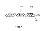
- FIG. 1 is a cross-sectional view showing a structure of a double sided printed circuit board of an embodiment of this invention.
- FIG. 2 (a) - (d) are cross-sectional views showing a method of manufacturing a double sided printed circuit board of an embodiment of this invention.
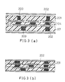
- FIG. 3 (a) and (b) are cross-sectional views showing a method of manufacturing a multilayer printed circuit board of an embodiment of this invention.
- FIG. 4 (a) and (b) are cross-sectional views showing a method of manufacturing a multilayer printed circuit board of another embodiment of this invention.
- FIG. 5 is a schematic view of a conductive particle used for a printed circuit board of an embodiment of this invention.
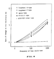
- FIG. 6 is a graph showing the relationship between the change of via hole connection resistance value in a heat cycle test and the frequency of the test in an embodiment of this invention, in which the via hole connection is achieved with paste containing different epoxy resins in a printed circuit board.
- FIG. 7 is a graph showing the relationship between the change of via hole connection resistance value in a heat cycle test and the frequency of the test in an embodiment of this invention, in which the via hole connection is achieved with paste containing epoxy resin in different mixing ratios in a printed circuit board.
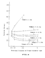
- FIG. 8 is a graph showing the relationship between the rotational frequency (shear) in an E-type viscometer and the viscosity of paste which includes a dispersant in different amounts.
- FIG. 1 is a cross-sectional view showing a structure of a double sided printed circuit board of an embodiment of this invention.
- a double sided printed circuit board 104 comprises a laminated base material 101, a copper foil 102 (In FIG. 1, a copper foil is formed into a circuit pattern), and a conductive via hole 103 in which a conductive paste has hardened.
- the major advantages of this invention are that a conductive paste can easily fill the holes due to its low viscosity and low volatility, and that the substrate has excellent reliability since the connection is achieved by a large amount of conductive filler.
- laminated base material 101 it is possible to use laminated base materials which are widely known at present.
- Examples are a glass-epoxy base material, an aramid-epoxy base material, and a paper phenol base material.
- the base material is called "prepreg" before being heated and pressurized and comprises a glass cloth or a nonwoven fabric as a core material which is impregnated with an uncured resin.
- the conductive filler As for the conductive filler, almost any kind of noble metals such as gold and silver or base metals such as copper, tin, nickel or lead can be used. In addition, not only pure metals can be used, but also alloyed metals or those comprising a metal or an insulating core covered with a conductive material as shown in FIG. 5.
- 501 denotes a spherical core
- 502 denotes a conductive material which covers the core surface and serves as the conductive filler.
- FIG. 2 (a) to (d) are views showing a method of manufacturing a double sided printed circuit board of this invention.
- a laminated base material 201 is a prepreg. This prepreg is disposed with through-holes. Usually, a drill is used for this step, but a laser beam can be used for processing specific materials.
- FIG. 2 (b) shows a state in which FIG. 2 (a) is positioned between two copper foils 202.
- FIG. 2 (c) shows a state after FIG. 2 (b) is heated and pressurized.
- FIG. 2 (c) shows a state in which the through-holes disposed in the prepreg have an increased density of metal filling after being heated and pressurized.
- FIG. 2 (d) shows a state after copper foil 202 on the surface is processed (e.g., etched) into circuit patterns. Copper foil 102 becomes a circuit conductor after being processed. After that, printed circuit boards used must be processed further prior to use, for example, applied with a solder resist, printed with letters and signs, or disposed with holes for insert components.
- FIGS. 3 (a) and (b) show a method of manufacturing a multilayer printed circuit board by repeatedly applying the above-mentioned method of manufacturing a double sided printed circuit board.
- FIG. 3 (a) shows a state in which a double sided circuit board 104 which serves as a core is positioned between substrates of FIG. 2 (a) having through-holes filled with conductive paste to which are further applied copper foils 202.
- a multilayer printed circuit board of FIG. 3 (b) is obtained which has already established an inner-via-hole connection.
- the copper foils on the upper and lower sides are patterned, a multilayer printed circuit board consisting of four layers is completed. After that, by repeating these steps, a multilayer printed circuit board with even more layers can be attained.
- the double sided printed circuit board used for the core was the double sided printed circuit board of this invention.
- this is not necessarily the case here. Instead, it is clear that a conventional through-hole double sided printed circuit board can be applied as well. In this case, it is better to fill the through-holes in advance.
- the through-hole substrate indicates a resin substrate, and not only can the through-hole substrate be used but also a ceramic substrate etc.
- FIGS. 4 (a) and (b) show another method of manufacturing a multilayer printed circuit board.
- a prepreg 201 which is filled with conductive paste 203 and is in the state before being heated and pressurized is positioned between two sheets of double sided printed circuit boards 104.
- a multilayer printed circuit board consisting of four layers of FIG. 4 (b) can be obtained.
- a multilayer printed circuit board consisting of more layers can be obtained by providing a plurality of double sided printed circuit boards, positioning the above-noted laminated substrates which are filled with a conductive filler and are in a state before being heated and pressurized between the double sided printed circuit boards, and heating and pressurizing.
- the double sided printed circuit board used was a double sided printed circuit board of this invention.
- a conventional through-hole double sided printed circuit board can be applied as well.
- the through-hole substrate be used but also a ceramic substrate etc.
- Epoxy resins used in the following embodiments are indicated below.
- a prepreg was an aramid epoxy sheet (TA-01 manufactured by Teijin Ltd.) of 200 ⁇ m in thickness. This prepreg was applied on one side with a 20 ⁇ m thick polyethylene terephthalate film by an adhesive and was disposed with through-holes of 0.2 mm in diameter by a drill.
- TA-01 manufactured by Teijin Ltd.
- Table 1 shows the form of the metal particle, the average size of the particle, the specific surface area, and the viscosity of the via hole filling paste of 0.5 rpm in an E-type viscometer at room temperature.
- Example Powder Form Average size of particle ⁇ m Specific surface area m 2 /g Paste viscosity Pa•sec Via resistance ⁇ 10 -5 ⁇ cm 1 silver spherical 0.2 3.14 2,300 6.3 2 0.5 1.35 1,050 1.2 3 1.0 0.62 620 0.3 4 2.0 0.30 480 0.3 5 5.0 0.16 320 0.4 6 10.0 0.10 100 0.6 7 flake 20.0 0.13 120 1.5 8 30.0 0.07 40 9.3 9 gold spherical 2.0 0.40 650 0.3 10 copper spherical 1.0 0.66 870 0.5 11 2.0 0.35 500 0.4 12 3.0 0.26 350 0.4 13 flake 10.0 0.20 400 1.5 14 nickel flake 5.0 0.32 680 2.7
- the prepreg filled with the paste was applied with copper foil 102 of 30 ⁇ m thickness on the upper and the lower sides. Then, this was formed into a double sided copper applied plate by heating and pressurizing 60 minutes at a temperature of 180°C and 50 Kg/cm 2 .
- electrode patterns were formed by using a conventional etching technique.
- Table 1 shows the resistance value of the inner-via-hole-connection conducted by using the respective paste. In all cases, a low resistance connection was obtained in which the resistivity value was ten times or less of the specific resistance value of the conductor although the paste included an insulating resin.
- the specific resistance value of each metal is (silver) 1.6 ⁇ 10 -6 ⁇ cm, (gold) 2.3 ⁇ 10 -6 ⁇ cm, and (nickel) 6.8 ⁇ 10 -6 ⁇ cm.
- the prepreg of a second embodiment had through-holes formed with 0.2 mm in diameter, and these through-holes were filled with conductive paste comprising metal particles of copper powder with an average particle size of 2 ⁇ m at 85 weight %, a resin selected from bisphenol A-type epoxy resin (EPICOAT 828 manufactured by Yuka Shell Epoxy Co., Ltd.), bisphenol F-type epoxy resin (EPICOAT 807 manufactured by Yuka Shell Epoxy Co., Ltd.), alicylic epoxy resin (ST-1000 manufactured by Tohto Kasei Co., Ltd.), amine-type epoxy resin (ELN-125 manufactured by Sumitomo Chemical Co., Ltd.), and epoxy resin composed of glycidyl esterificated dimer acids at 12 weight %, and an amine adduct hardener (PN-23 manufactured by Ajinomoto Co., Ltd.) at 3 weight %.
- a resin selected from bisphenol A-type epoxy resin EPICOAT 828 manufactured by Yuka Shell Epoxy Co., Ltd.
- Example Resin Paste viscosity Pa•sec Volatile amount WT% Via resistance ⁇ 10 -5 ⁇ cm 1 bisphenol A-type 1,500 0.16 0.4 2 bisphenol F-type 800 0.15 0.4 3 alicyclic epoxy 200 0.30 0.7 4 amine-type epoxy 60 0.30 0.6 5 glycidyl ester type 80 0.40 0.4
- the prepreg having holes was filled with the paste and copper foil 102 was applied on the upper and the lower sides. Then, this was formed into a double sided copper applied plate by heating and pressurizing 60 minutes at 180°C and 50 Kg/cm 2 . Electrode patterns were formed by using a conventional etching technique.
- Table 2 shows the resistance value of the inner-via-hole-connection conducted by using the respective paste. In all cases, a low resistance connection was obtained in which the resistivity value was ten times or less of the specific resistance value of the conductor although the paste included an insulating resin.
- FIG. 6 shows the change of the via hole connection resistance value in a heat cycle test (-55°C ⁇ 125°C, 30 minutes each) up to 1000 cycles.
- the change of the via hole resistance value in each paste sample was 10 percent or less against the initial resistance value, so the reliability of the via hole was not ruined.
- the glycidyl ester type showed a rate of change at 1 % or less. Due to the flexibility of the resin, only a slight change occurred against a thermal shock, and the reliability of the via-hole-connection was extremely good.
- the prepreg of a third embodiment had through-holes formed with 0.2 mm in diameter, and these through-holes were filled with conductive paste comprising metal particles of copper powder with an average particle size of 2 ⁇ m at 85 weight %, a blended resin consisting of one resin selected from Group A (bisphenol A-type epoxy resin, bisphenol F-type epoxy resin) and one resin selected from Group B (alicylic epoxy resin, amine-type epoxy resin, or epoxy resin composed of glycidyl esterificated dimer acids) at 12 gross weight %, and an amine adduct hardener (MY-24) at 3 weight %. They were mixed and kneaded on three roles.
- conductive paste comprising metal particles of copper powder with an average particle size of 2 ⁇ m at 85 weight %
- a blended resin consisting of one resin selected from Group A (bisphenol A-type epoxy resin, bisphenol F-type epoxy resin) and one resin selected from Group B (alicylic epoxy resin, amine-type epoxy resin, or epoxy resin composed of
- Table 3 shows the viscosity of the via hole filling paste of 0.5 rpm in an E-type viscometer at room temperature.
- Example Resin A WT% Resin B WT% Paste viscosity Pa•sec Via resistance ⁇ 10 -5 ⁇ cm 1 bisphenol A-type 50 alicyclic 50 720 0.8 2 50 amine-type 50 540 0.6 3 75 glycidyl ester 25 1,060 0.5 5 50 50 660 0.5 6 25 75 75 380 0.4 7 bisphenol F-type 75 glycidyl ester 25 620 0.5 9 50 50 400 0.4 10 25 75 220 0.4
- the prepreg filled with this paste was applied with copper foil 102 on the upper and the lower sides. Then, this was formed into a double sided copper applied plate by heating and pressurizing 60 minutes at 180°C and 50 Kg/cm 2 . Electrode patterns were formed by using a conventional etching technique.
- Table 3 shows the resistance value of the inner-via-hole-connection conducted by using the respective paste. In all cases, a low resistance connection was obtained in which the resistivity value was ten times or less of the specific resistance value of the conductor although the paste included an insulating resin.
- FIG. 7 shows the change of the via hole resistance value in a heat cycle test (-55°C ⁇ 125°C, 30 minutes each) up to 1000 cycles.
- the change of the via hole resistance value in each paste sample was 10 percent or less against the initial resistance value, so the reliability of the via hole was not ruined.
- the glycidyl ester mixed type showed a rate of change at 1 % or less at the amount content of 50 weight % or more, thereby maintaining the reliability of the via-hole-connection.
- the prepreg of a fourth embodiment had through-holes formed with 0.2 mm in diameter, and these through-holes were filled with conductive paste comprising metal particles of silver powder or copper powder with an average particle size of 2 ⁇ m at 75 to 92.5 weight %, a blended resin consisting of bisphenol A-type epoxy resin and epoxy resin composed of glycidyl esterificated dimer acids in 25 to 75 weight ratio at 4.5 to 22 gross weight %, and an amine adduct hardener (MY-24) at 3 weight %. They were mixed and kneaded on three roles. Table 4 shows the viscosity of the via hole filling paste at room temperature.
- the prepreg filled with this paste was applied with copper foil 102 on the upper and the lower sides. Then, this was formed into a double sided copper applied plate by heating and pressurizing 60 minutes at 180°C and 50 Kg/cm 2 . Electrode patterns were formed by using a conventional etching technique.
- Table 4 shows the resistance value of the inner-via-hole-connection conducted by using the respective paste. In all cases, a low resistance connection was obtained in which the resistivity value was ten times or less of the specific resistance value of the conductor although the paste included an insulating resin. On the other hand, when the metal content was 80 weight % or less, the via hole resistance value was large due to the lack of the conductive metal. Furthermore, when the metal content was 92 weight % or more, the via hole filling was difficult to conduct due to high paste viscosity.
- the prepreg of a fifth embodiment had through-holes formed with 0.2 mm in diameter, and these through-holes were filled with conductive paste comprising metal particles of silver powder or copper powder with an average particle size of 2 ⁇ m at 85 weight %, a blended resin consisting of bisphenol A-type epoxy resin and epoxy resin composed of glycidyl esterificated dimer acids in 25 to 75 weight ratio at 12 gross weight %, and dicyandiamide (DICY7 manufactured by Yuka Shell Epoxy Co., Ltd.) or acid anhydride (RIKACID MH manufactured by New Japan Chemical Co., Ltd.) or amine adduct hardener (PN-23, MY-24 manufactured by Ajinomoto Co., Ltd.) at 3 weight %.
- conductive paste comprising metal particles of silver powder or copper powder with an average particle size of 2 ⁇ m at 85 weight %
- a blended resin consisting of bisphenol A-type epoxy resin and epoxy resin composed of glycidyl esterificated dimer acids in 25
- Table 5 shows the viscosity of the via hole filling paste at room temperature and the volatile amount of the paste when heated to 300°C at a rate of 10°C/min.
- Example Metal Hardener Paste viscosity Pa ⁇ sec Volatile amount WT% Via resistance ⁇ 10 -5 ⁇ cm 1 silver dicyandiamide 520 0.32 0.4 2 acid anhydride 200 1.50 0.5 3 amine adduct(MY-24) 620 0.50 0.4 4 amine adduct(PN-23) 600 0.42 0.4 5 copper dicyandiamide 380 0.35 0.4 6 acid anhydride 120 1.56 0.5 7 amine adduct(MY-24) 430 0.50 0.4 8 amine adduct(PN-23) 450 0.40 0.4
- the prepreg filled with this paste was applied with copper foil 102 on the upper and the lower sides. Then, this was formed into a double sided copper applied plate by heating and pressurizing 60 minutes at 180°C and 50 Kg/cm 2 . Electrode patterns were formed by using a conventional etching technique.
- Table 5 shows the resistance value of the inner-via-hole-connection conducted by using the respective paste. Regardless of the hardener type, a low resistance connection was obtained in which the resistivity value was ten times or less of the specific resistance value of the conductor although the paste included an insulating resin.
- the prepreg of a sixth embodiment had through-holes formed with 0.2 mm in diameter, and these through-holes were filled with conductive paste comprising metal particles of copper powder with an average particle size of 2 ⁇ m at 85 weight %, a blended resin consisting of bisphenol A-type epoxy resin and epoxy resin composed of glycidyl esterificated dimer acids in 25 to 75 weight ratio at 8 to 14.5 gross weight %, and phthalic anhydride or amine adduct type hardener (MY-24) at 0.5 to 7 weight %. They were mixed and kneaded and mixed on three roles.
- Table 6 shows the viscosity of the via hole filling paste at room temperature and the volatile amount of the paste when heated to 300°C at a rate of 10°C/min.
- Example Hardener Amount of hardener WT% Paste viscosity Pa ⁇ sec Volatile amount WT% Via resistance ⁇ 10 -5 ⁇ cm 1 acid anhydride 0.5 160 0.60 0.8 2 3.0 120 1.56 0.5 3 5.0 120 1.95 0.4 4 7.0 110 2.34 - 5 amine adduct 0.5 180 0.40 0.4 6 3.0 450 0.40 0.4 7 5.0 850 0.38 0.5 8 7.0 2,400 0.35 20.0
- the prepreg filled with this paste was applied with copper foil 102 on the upper and the lower sides. Then, this was formed into a double sided copper applied plate by heating and pressurizing 60 minutes at 180°C and 50 Kg/cm 2 . Electrode patterns were formed by using a conventional etching technique.
- Table 6 shows the resistance value of the inner-via-hole-connection conducted by using the respective paste. Regardless of the hardener type, a low resistance connection was obtained in which the resistivity value was ten times or less of the specific resistance value of the conductor although the paste included an insulating resin. However, when too much solid powder such as an amine adduct hardener was added, the viscosity increased, so the via hole filling was difficult to conduct by using the paste added with a hardener of 5 weight % or more. Furthermore, when the paste using a hardener with high volatility such as acid anhydride had a volatile amount of more than 2 weight %, a double sided copper applied plate of satisfactory quality was not obtained due to swelling of the substrate and the electrode.
- the prepreg of a seventh embodiment had through-holes formed with 0.2 mm in diameter, and these through-holes were filled with conductive paste comprising metal particles of copper powder with an average particle size of 2 ⁇ m having different surface oxygen amounts at 85 weight %, a blended resin consisting of bisphenol A-type epoxy resin and epoxy resin composed of glycidyl esterificated dimer acids in 25 to 75 weight ratio at 12 gross weight %, and an amine adduct hardener (MY-24) at 3 weight %. They were mixed and kneaded on three roles. Table 7 shows the viscosity of the via hole filling paste at room temperature.
- the prepreg filled with this paste was applied with copper foil 102 on the upper and the lower sides. Then, this was formed into a double sided copper applied plate by heating and pressurizing 60 minutes at 180°C and 50 Kg/cm 2 . Electrode patterns were formed by using a conventional etching technique.
- Table 7 shows the resistance value of the inner-via-hole-connection conducted by using the respective paste.
- the conductive paste used here comprised metal particles of copper powder with an average particle size of 2 ⁇ m at 85 weight %, a blended resin consisting of bisphenol A-type epoxy resin and epoxy resin composed of glycidyl esterificated dimer acids in 25 to 75 weight ratio at 12 gross weight %, and an amine adduct hardener (MY-24) at 3 weight %.
- the components had been mixed and kneaded on three roles.
- An aramid-epoxy prepreg was disposed with through-holes of 0.2 mm in diameter which were filled with the above-mentioned paste. This aramid-epoxy prepreg was positioned between two sheets of aramid-epoxy double sided substrates having patterns formed for the connection resistance measurement. Then, this was formed into a four-layer printed circuit board by heating and pressurizing 60 minutes at 180°C and 50 Kg/cm 2 .
- the inner-via-hole connection resistance formed between the second and the third layer of the four-layer substrate showed the same resistance value as in the first embodiment. Also, a six-layer printed circuit board attained the same reliability with the same connection resistance value as in the four-layer printed circuit board.
- the above-mentioned paste was used for manufacturing an aramid-epoxy double sided substrate with the same method as in Example 1.
- One sheet of this substrate was positioned between two sheets of aramid-epoxy prepregs having through-holes of 0.2 mm in diameter filled with the above-noted paste.
- equivalent resistance was obtained for the via-hole-connection.
- the same reliability was obtained in a six-layer printed circuit board manufactured by using this method.
- a ceramic substrate with circuits was used instead of the aramid-epoxy double sided substrate manufactured by the same method as in Example 1, and the same reliability was obtained for the via-hole-connection resistance.
- the prepreg was an aramid-epoxy sheet (TA-01 manufactured by Teijin Ltd.) of 200 ⁇ m in thickness. This prepreg was applied on one side with a 20 ⁇ m thick polyethylene terephthalate film by an adhesive and was disposed with through-holes of 0.2 mm in diameter by a drill.
- TA-01 manufactured by Teijin Ltd.
- via hole filling paste comprising metal particles of silver, gold, copper and nickel in a spherical and flake form at 85 weight %, a resin composition of bisphenol A-type epoxy resin (EPICOAT 828 manufactured by Yuka Shell Epoxy Co., Ltd.) at 3 weight %, an epoxy resin composed of glycidyl esterificated dimer acids (YD-171 manufactured by Tohto Kasei Co., Ltd.) at 9 weight %, an amine adduct hardener (MY-24 manufactured by Ajinomoto Co., Ltd.) at 3 weight %, and a dispersant at 0.01 to 2.0 weight % against the gross amount of the metal, the resin, and the hardener comprising one dispersant selected from polyoxyethylene sorbitan fatty acid ester (nonionic surface active agent "SOLGEN” TW manufactured by Dai-ichi Kogyo Seiyaku Co., Ltd.), phosphate (anion surface active agent "PLYSU
- Table 8 shows the form of the metal particles, the average size of the particles, the specific surface area, the type of the dispersant and its compounded amount (weight %), and the viscosity of the via hole filling paste of 0.5 rpm in an E-type viscometer at room temperature.
- the prepreg filled with the paste was applied with copper foil 102 of 35 ⁇ m thick on the upper and the lower sides. Then, this was formed into a double sided copper applied plate by heating and pressurizing 60 minutes at 180°C and 50 Kg/cm 2 .
- electrode patterns were formed by using a conventional etching technique.
- Table 8 shows the resistance value of the inner-via-hole-connection conducted by using the respective paste. In all cases, a low resistance connection was obtained in which the resistivity value was ten times or less of the specific resistance value of the conductor although the paste included an insulating resin.
- the specific resistance value of each metal used in this embodiment is: silver (1.6 ⁇ 10 -6 ⁇ cm), gold (2.3 ⁇ 10 -6 ⁇ cm), copper (1.7 ⁇ 10 -6 ⁇ cm), and nickel (6.8 ⁇ 10 -6 ⁇ cm).
- the change of the paste viscosity is shown in FIG. 8 in which shear is provided to the paste by changing the frequency with an E-type viscometer. It is desirable for a filling paste that the viscosity decreases under high shear in a printing process compared to under the condition of no shear. In the examples without dispersant added the viscosity increased when provided with shear, so it was difficult to fill the paste. On the other hand, the examples with dispersant added made a small increase in the viscosity under high shear, and for those added more than 0.5 weight part the viscosity decreased under high shear. Accordingly, the filling became easier to conduct. However, the examples with dispersant added 2.0 weight % or more had the connection of the metal particles disturbed, so the via connection resistance increased.
- the prepreg of a tenth embodiment had through-holes formed with 0.2 mm in diameter, and these through-holes were filled with conductive paste comprising metal particles of copper powder with an average size of 2 ⁇ m at 85 weight %, a resin selected from bisphenol A-type epoxy resin, bisphenol F-type epoxy resin (EPICOAT 807 manufactured by Yuka Shell Epoxy Co., Ltd.), alicylic epoxy resin (ST-1000 manufactured by Tohto Kasei Co., Ltd.), amine type epoxy resin (ELN-125 manufactured by Sumitomo Chemical Co., Ltd.), and an epoxy resin composed of glycidyl esterificated dimer acids at 12 weight %, an amine adduct hardener (PN-23 manufactured by Ajinomoto Co., Ltd.) at 3 weight %, and a dispersant containing phosphate (“PLYSURF" manufactured by Dai-ichi Kogyo Seiyaku Co., Ltd.) contained at 0.2 weight % against the
- Example Resin Paste viscosity Pa•sec Volatile amount WT% Via resistance ⁇ 10 -5 ⁇ cm 1 bisphenol A-type 1,350 0.16 0.4 2 bisphenol F-type 720 0.15 0.4 3 alicyclic epoxy 180 0.30 0.8 4 amine-type epoxy 50 0.30 0.6 5 glycidyl ester type 60 0.40 0.6
- the prepreg having holes was filled with the paste and applied with copper foil 102 on the upper and the lower sides. Then, this was formed into a double sided copper applied plate by heating and pressurizing 60 minutes at 180°C and 50 Kg/cm 2 . Electrode patterns were formed by using a conventional etching technique.
- Table 9 shows the resistance value of the inner-via-hole-connection conducted by using the respective paste. In all cases, a low resistance connection was obtained in which the resistivity value was ten times or less of the specific resistance value of the conductor although the paste included an insulating resin.
- the prepreg of an eleventh embodiment had through-holes formed with 0.2 mm in diameter, and these through-holes were filled with conductive paste comprising metal particles of copper powder with an average particle size of 2 ⁇ m at 85 weight %, a blended resin consisting of one epoxy resin selected from Group A (bisphenol A-type epoxy resin, bisphenol F-type epoxy resin) and one selected from Group B (alicylic epoxy resin, amine-type epoxy resin, epoxy resin composed of glycidyl esterificated dimer acids) at 12 gross weight %, an amine adduct hardener (MY-24) at 3 weight %, and a dispersant containing phosphate ("PLYSURF" manufactured by Dai-ichi Kogyo Seiyaku Co., Ltd.) at 0.2 weight % against the gross amount of the metal, the resin, and the hardener.
- a blended resin consisting of one epoxy resin selected from Group A (bisphenol A-type epoxy resin, bisphenol F-type epoxy resin) and one selected from Group B
- An aramid-epoxy prepreg comprised a prepreg disposed with through-holes of 0.2 mm in diameter which were filled with the above-mentioned paste.
- Table 10 shows the viscosity of the via hole filling paste of 0.5 rpm in an E-type viscometer at room temperature.
- the prepreg filled with this paste was applied with copper foil 102 on the upper and the lower sides. Then, this was formed into a double sided copper applied plate by heating and pressurizing 60 minutes at 180°C and 50 Kg/cm 2 . Electrode patterns were formed by using a conventional etching technique.
- Table 10 shows the resistance value of the inner-via-hole-connection conducted by using the respective paste. A low resistance connection was obtained in which the resistivity value was ten times or less of the specific resistance value of the conductor although the paste included an insulating resin.
- the prepreg of a twelfth embodiment had through-holes formed with 0.2 mm in diameter, and these through-holes were filled with conductive paste comprising metal particles of silver powder or copper powder with an average particle size of 2 ⁇ m at 75 to 93.0 weight %, a blended resin consisting of bisphenol A-type epoxy resin and epoxy resin composed of glycidyl esterificated dimer acids in 25 to 75 weight ratio at 4.0 to 22 gross weight %, an amine adduct hardener (MY-24) at 3 weight %, and a dispersant containing phosphate ("PLYSURF" manufactured by Dai-ichi Kogyo Seiyaku Co., Ltd.) at 0.2 weight % against the gross amount of the metal, the resin, and the hardener.
- conductive paste comprising metal particles of silver powder or copper powder with an average particle size of 2 ⁇ m at 75 to 93.0 weight %
- a blended resin consisting of bisphenol A-type epoxy resin and epoxy resin composed of
- Table 11 shows the viscosity of the via hole filling paste at room temperature.
- Example Metal weight WT% Resin WT% Paste viscosity Pa•sec Via resistance ⁇ 10 -5 ⁇ cm 1 silver 80.0 bisphenol A (25WT%) + glycidyl ester (75WT%) 17 250 0.7 2 85.0 12 480 0.4 3 copper 75.0 bisphenol A (25WT%) + glycidyl ester (75WT%) 22 40 5.0 4 80.0 17 180 0.7 5 85.0 12 380 0.4 6 90.0 7 890 0.4 7 92.0 5 1,450 0.3 8 92.5 4.5 1,880 0.4 9 93.0 4 2,680 -
- the prepreg filled with this paste was applied with copper foil 102 on the upper and the lower sides. Then, this was formed into a double sided copper applied plate by heating and pressurizing 60 minutes at 180°C and 50 Kg/cm 2 . Electrode patterns were formed by using a conventional etching technique.
- Table 11 shows the resistance value of the inner-via-hole-connection conducted by using the respective paste.
- a low resistance connection was obtained in which the resistivity value was ten times or less of the specific resistance value of the conductor although the paste included an insulating resin.
- the via hole resistance value was large due to the lack of the conductive metal.
- the via hole filling was difficult to conduct due to high paste viscosity.
- the prepreg of a thirteenth embodiment had through-holes formed with 0.2 mm in diameter, and these through-holes were filled with conductive paste comprising metal particles of silver powder or copper powder with an average particle size of 2 ⁇ m at 85 weight %, a blended resin consisting of bisphenol A-type epoxy resin and epoxy resin composed of glycidyl esterificated dimer acids in 25 to 75 weight ratio at 12 gross weight %, a hardener selected from dicyandiamide (DICY7 manufactured by Yuka Shell Epoxy Co., Ltd.) or acid anhydride (RIKACID MH manufactured by New Japan Chemical Co., Ltd.) or amine adduct hardener (PN-23, MY-24 manufactured by Ajinomoto Co., Ltd.) at 3 weight %, and a dispersant containing phosphate ("PLYSURF" manufactured by Dai-ichi Kogyo Seiyaku Co., Ltd.) at 0.2 weight % against the gross amount of the metal, the
- Table 12 shows the viscosity of the via hole filling paste at room temperature (25°C) and the volatile amount of the paste when heated to 300°C at a rate of 10°C/min.
- Example Metal Hardener Paste viscosity Pa•sec Volatile amount WT% Via resistance ⁇ 10 -5 ⁇ cm 1 silver dicyandiamide 470 0.32 0.4 2 acid anhydride 180 1.50 0.4 3 amine adduct(MY-24) 540 0.50 0.4 4 amine adduct(PN-23) 520 0.42 0.4 5 copper dicyandiamide 320 0.35 0.4 6 acid anhydride 100 1.56 0.5 7 amine adduct(MY-24) 380 0.50 0.4 8 amine adduct(PN-23) 380 0.40 0.4
- the prepreg filled with this paste was applied with copper foil 102 on the upper and the lower sides. Then, this was formed into a double sided copper applied plate by heating and pressurizing 60 minutes at 180°C and 50 Kg/cm 2 . Electrode patterns were formed by using a conventional etching technique.
- Table 12 shows the resistance value of the inner-via-hole-connection conducted by using the respective paste. Regardless of the hardener type, a low resistance connection was obtained in which the resistivity value was ten times or less of the specific resistance value of the conductor although the paste included an insulating resin.
- the prepreg of a fourteenth embodiment had through-holes formed with 0.2 mm in diameter, and these through-holes were filled with conductive paste comprising metal particles of silver powder or copper powder with an average particle size of 2 ⁇ m at 85 weight %, a blended resin consisting of bisphenol A-type epoxy resin and epoxy resin composed of glycidyl esterificated dimer acids in 25 to 75 weight ratio at 8 to 14.5 gross weight %, a phthalic anhydride or amine adduct hardener (MY-24) at 0.5 to 7 weight %, and a dispersant containing phosphate ("PLYSURF" manufactured by Dai-ichi Kogyo Seiyaku Co., Ltd.) at 0.2 weight % against the gross amount of the metal, the resin, and the hardener.
- conductive paste comprising metal particles of silver powder or copper powder with an average particle size of 2 ⁇ m at 85 weight %
- a blended resin consisting of bisphenol A-type epoxy resin and epoxy resin composed of g
- Table 13 shows the viscosity of the via hole filling paste at room temperature and the volatile amount of the paste when heated to 300°C at a rate of 10°C/min.
- Example Hardener Amount of hardener WT% Paste viscosity Pa•sec Volatile amount WT% Via resistance ⁇ 10 -5 ⁇ cm 1 acid anhydride 0.5 140 0.60 0.9 2 3.0 100 1.58 0.5 3 5.0 110 1.95 0.4 4 7.0 110 2.34 - 5 amine adduct 0.5 170 0.40 0.5 6 3.0 410 0.40 0.5 7 5.0 720 0.38 0.5 8 7.0 2,100 0.35 15.0
- the prepreg filled with this paste was applied with copper foil 102 on the upper and the lower sides. Then, this was formed into a double sided copper applied plate by heating and pressurizing 60 minutes at 180°C and 50 Kg/cm 2 . Electrode patterns were formed by using a conventional etching technique.
- Table 13 shows the resistance value of the inner-via-hole-connection conducted by using the respective paste. Regardless of the weight ratio of the hardener, a low resistance connection was obtained in which the resistivity value was ten times or less of the specific resistance value of the conductor although the paste included an insulating resin. However, when too much solid powder such as an amine adduct hardener was added, the viscosity increased, so the via hole filling was difficult to conduct by using the paste added with a hardener of 5 weight % or more. Furthermore, when the paste using a hardener with high volatility such as acid anhydride had a volatile amount of more than 2 weight %, a double sided copper applied plate of satisfactory quality was not obtained due to swelling of the substrate and the electrode.
- the prepreg of a fifteenth embodiment had through-holes formed with 0.2 mm in diameter, and these through-holes were filled with conductive paste comprising metal particles of copper powder with an average particle size of 2 ⁇ m having different surface oxygen amounts at 85 weight %, a blended resin consisting of bisphenol A-type epoxy resin and epoxy resin composed of glycidyl esterificated dimer acids in 25 to 75 weight ratio at 12 gross weight %, an amine adduct hardener (MY-24) at 3 weight %, and a dispersant containing phosphate ("PLYSURF" manufactured by Dai-ichi Kogyo Seiyaku Co., Ltd.) at 0.2 weight % against the gross amount of the metal, the resin, and the hardener.
- conductive paste comprising metal particles of copper powder with an average particle size of 2 ⁇ m having different surface oxygen amounts at 85 weight %
- a blended resin consisting of bisphenol A-type epoxy resin and epoxy resin composed of glycidyl esterificated dimer
- Table 14 shows the viscosity of the via hole filling paste at room temperature.
- the prepreg filled with this paste was applied with copper foil 102 on the upper and the lower sides. Then, this was formed into a double sided copper applied plate by heating and pressurizing 60 minutes at 180°C and 50 Kg/cm 2 . Electrode patterns were formed by using a conventional etching technique.
- Table 14 shows the resistance value of the inner-via-hole-connection conducted by using the respective paste.
- Conductive paste used here comprised metal particles of copper powder with an average particle size of 2 ⁇ m at 85 weight %, a blended resin consisting of bisphenol A-type epoxy resin and epoxy resin composed of glycidyl esterificated dimer acids in 25 to 75 weight ratio at 12 gross weight %, an amine adduct hardener (MY-24) at 3 weight %, and a dispersant containing phosphate ("PLYSURF" manufactured by Dai-ichi Kogyo Seiyaku Co., Ltd.) at 0.2 weight % against the gross amount of the metal, the resin, and the hardener. They were mixed and kneaded on three roles.
- An aramid-epoxy prepreg was disposed with through-holes of 0.2 mm in diameter which were filled with the above-mentioned paste.
- This aramid-epoxy prepreg was positioned between two sheets of aramid-epoxy double sided substrates having patterns formed for the connection resistance measurement. Then, this was formed into a four-layer printed circuit board by heating and pressurizing 60 minutes at 180°C and 50 Kg/cm 2 .
- the inner-via-hole connection resistance formed between the second and the third layer of the four-layer substrate showed the same resistance value as in the first embodiment. Also, a six-layer printed circuit board attained the same reliability with the same connection resistance value as in the four-layer printed circuit board.
- the above-mentioned paste was used for manufacturing an aramid-epoxy double sided substrate with the same method as in Example 8.
- One sheet of this substrate was positioned between two sheets of aramid-epoxy prepregs having through-holes of 0.2 mm in diameter filled with the above-noted paste.
- equivalent resistance was obtained for the via-hole-connection.
- the same reliability was obtained in a six-layer printed circuit board manufactured by using this method.
- a ceramic substrate with circuits was used instead of the aramid-epoxy double sided substrate manufactured by the same method as in Example 8, and the same reliability was obtained for the via-hole-connection resistance.
- a double sided printed circuit board As described above, similar to a double sided printed circuit board, a multilayer printed circuit board, and methods of manufacturing the same with use of the via hole filling paste of this invention, and a double sided printed circuit board with inner via holes can be attained without using a through-hole plating technique. Furthermore, this circuit board can be formed into a multilayer printed circuit board easily.
Landscapes
- Engineering & Computer Science (AREA)
- Microelectronics & Electronic Packaging (AREA)
- Chemical & Material Sciences (AREA)
- Dispersion Chemistry (AREA)
- Manufacturing & Machinery (AREA)
- Physics & Mathematics (AREA)
- Spectroscopy & Molecular Physics (AREA)
- Printing Elements For Providing Electric Connections Between Printed Circuits (AREA)
- Conductive Materials (AREA)
Claims (18)
- Composition de pâte conductrice pour remplir des trous d'interconnexion comprenant (a) une charge conductrice à raison de 80 à 92 pour-cent en poids, ayant une granulométrie moyenne de 0,5 à 20 µm et une surface spécifique de 0,1 à 1,5 m2/g, (b) une résine époxyde liquide, à raison de 4,5 à 19,5 pour-cent en poids, contenant deux groupes époxyde ou davantage, comprenant au moins 10 % en poids d'une résine époxyde qui comprend des glycidyle esters d'acides gras dimérisés, et ayant une viscosité à la température ambiante de 15 Pa.sec ou moins et (c) un agent de durcissement, à raison de 0,5 à 5 pour-cent en poids, où la composition de pâte conductrice a une viscosité de 2000 Pa.sec ou moins et contient 2,0 pour-cent en poids ou moins de composants volatiles.
- Pâte conductrice selon la revendication 1, comprenant en outre un dispersant, à raison de 0,01 à 1,5 parties en poids pour 100 parties en poids desdits composants (a) à (c).
- Pâte conductrice selon la revendication 1 ou 2, où ladite charge conductrice comprend au moins une substance choisie parmi l'or, l'argent, le palladium, le cuivre, le nickel, l'étain et le plomb, sous la forme de grains fins.
- Pâte conductrice selon la revendication 1, 2 ou 3, où ladite charge conductrice comprend du cuivre ayant une concentration en oxygène de surface de 1,0 pour-cent en poids ou moins.
- Pâte conductrice selon l'une quelconque des revendications 1 à 4, où ladite résine époxyde comprend au moins une résine époxyde liquide choisie parmi les résines époxyde à base de bisphénol A, les résines époxyde à base de bisphénol F, les résines époxyde alicycliques, les résines époxyde à base d'amines et les résines époxyde à base de glycidyle esters.
- Pâte conductrice selon l'une quelconque des revendications 1 à 5, où ladite résine époxyde liquide est un composé comprenant 50 % en poids ou moins d'une résine époxyde choisie parmi les résines époxyde à base de bisphénol A et les résines époxyde à base de bisphénol F et comprendant, en outre, 50 pour-cent en poids ou plus, d'une résine époxyde à base de glycidyle ester d'acides gras dimérisés, avec un équivalent en groupes époxyde de 300 à 600 g/éq.
- Pâte conductrice selon l'une quelconque des revendications 1 à 6, où ledit agent de durcissement est au moins un agent de durcissement choisi parmi les agents de durcissement dérivés d'amines, de l'urée, d'anhydrides d'acide et d'amines aromatiques.
- Pâte conductrice selon l'une quelconque des revendications 1 à 7, où ledit agent de durcissement comprend un agent de durcissement latent.
- Pâte conductrice selon l'une quelconque des revendications 2 à 8, où ledit dispersant comprend au moins un dispersant choisi parmi les dispersants non ioniques, les dispersants anioniques et les dispersants cationiques du type sel d'ammonium quaternaire.
- Utilisation de la pâte conductrice selon l'une quelconque des revendications 1 à 9 pour remplir des trous traversants dans le matériau de base isolant de plaquettes à circuits imprimés.
- Plaquette à circuits imprimés sur les deux côtés comprenant un matériau de base isolant pourvu de trous d'interconnexion interne qui sont remplis avec la pâte conductrice selon l'une quelconque des revendications 1 à 9 et pressée à chaud et durcie, où des couches des électrodes inférieure et supérieure, présentes sur la surface dudit matériau de base isolant, sont connectées électriquement.
- Plaquette à couches multiples de circuits imprimés comprenant une pluralité de couches de matériau de base isolant et deux couches d'électrodes ou davantage, où chaque matériau de base isolant est pourvu de trous d'interconnexion internes remplis avec la pâte conductrice selon l'une quelconque des revendications 1 à 9 et pressée à chaud et durcie, où chaque couche d'électrode est connectée électriquement.
- Plaquette à circuits imprimés selon la revendication 11 ou 12, où ledit matériau de base isolant comprend un matériau composite constitué de fibres d'aramide et d'une résine thermodurcissable.
- Plaquette à circuits imprimés selon la revendication 11 ou 12, où ledit matériau de base isolant comprend un matériau composite constitué d'un non tissé d'aramide et d'une résine époxyde.
- Procédé de fabrication d'une plaquette à circuits imprimés sur les deux côtés, comprenant les étapes consistant à :réaliser des trous d'interconnexion dans un préimprégné utilisé pour la fabrication d'une plaquette à circuits imprimés;remplir les trous d'interconnexion avec une pâte conductrice selon l'une quelconque des revendications 1 à 9;placer ledit préimprégné entre des feuilles de cuivre sur les couches supérieure et inférieure et appliquer de la chaleur et de la pression; etformer des circuits par une attaque des feuilles de cuivre.
- Procédé de fabrication d'une plaquette à couches multiples de circuits imprimés, comprenant les étapes consistant à :réaliser des trous d'interconnexion dans un préimprégné utilisé pour la fabrication d'une plaquette à circuits imprimés;remplir les trous d'interconnexion avec une pâte conductrice selon l'une quelconque des revendications 1 à 9;placer ledit préimprégné au-dessus et en dessous d'une plaquette à circuits imprimés sur les deux côtés;placer lesdits préimprégnés entre des feuilles de cuivre sur les couches supérieures, appliquer de la chaleur et de la pression, et effectuer une attaque sur les feuilles de cuivre; ouappliquer de la chaleur et de la pression et former les circuits.
- Procédé selon la revendication 15 ou 16, où ledit préimprégné comprend un matériau composite constitué par des fibres d'aramide et une résine thermodurcissable.
- Procédé selon la revendication 15 ou 16, où ledit préimprégné comprend une feuille en un non tissé d'aramide imprégné avec une résine époxyde thermodurcissable.
Applications Claiming Priority (4)
| Application Number | Priority Date | Filing Date | Title |
|---|---|---|---|
| JP27261893 | 1993-10-29 | ||
| JP272619/93 | 1993-10-29 | ||
| JP272618/93 | 1993-10-29 | ||
| JP27261993 | 1993-10-29 |
Publications (2)
| Publication Number | Publication Date |
|---|---|
| EP0651602A1 EP0651602A1 (fr) | 1995-05-03 |
| EP0651602B1 true EP0651602B1 (fr) | 1999-04-07 |
Family
ID=26550292
Family Applications (1)
| Application Number | Title | Priority Date | Filing Date |
|---|---|---|---|
| EP94117098A Expired - Lifetime EP0651602B1 (fr) | 1993-10-29 | 1994-10-28 | Composition d'une pâte conductrice pour le remplissage de trous de contact, plaque de circuit imprimé en utilisant cette pâte conductrice, et procédé de sa production |
Country Status (3)
| Country | Link |
|---|---|
| US (4) | US5652042A (fr) |
| EP (1) | EP0651602B1 (fr) |
| DE (1) | DE69417684T2 (fr) |
Cited By (2)
| Publication number | Priority date | Publication date | Assignee | Title |
|---|---|---|---|---|
| WO2017207078A1 (fr) | 2016-06-03 | 2017-12-07 | Häusermann GmbH | Procédé de fabrication d'une carte de circuit imprimé multicouche avec interconnexion de couches internes, carte de circuit imprimé multicouche et installation pour sa fabrication |
| EP4270459A4 (fr) * | 2020-12-28 | 2024-07-03 | Suzhou Institute of Nano-Tech and Nano-Bionics (SINANO), Chinese Academy of Sciences | Structure d'interconnexion d'électrodes, son procédé de fabrication et son application |
Families Citing this family (116)
| Publication number | Priority date | Publication date | Assignee | Title |
|---|---|---|---|---|
| US5484647A (en) * | 1993-09-21 | 1996-01-16 | Matsushita Electric Industrial Co., Ltd. | Connecting member of a circuit substrate and method of manufacturing multilayer circuit substrates by using the same |
| CN1044762C (zh) | 1993-09-22 | 1999-08-18 | 松下电器产业株式会社 | 印刷电路板及其制造方法 |
| US5652042A (en) * | 1993-10-29 | 1997-07-29 | Matsushita Electric Industrial Co., Ltd. | Conductive paste compound for via hole filling, printed circuit board which uses the conductive paste |
| US5780143A (en) * | 1995-03-01 | 1998-07-14 | Tokuyama Corporation | Circuit board |
| US5575956A (en) * | 1995-07-19 | 1996-11-19 | Hughes Aircraft Company | Room-temperature stable, one-component, electrically-conductive, flexible epoxy adhesives |
| US5837356A (en) * | 1995-09-22 | 1998-11-17 | Kyocera Corporation | Wiring board and method for manufacturing the same |
| US5829694A (en) | 1996-01-04 | 1998-11-03 | Resource Concepts, Inc. | Apparatus and systems that separate and isolate precious and semi-precious metals from electronic circuit boards |
| US6320140B1 (en) * | 1996-06-14 | 2001-11-20 | Ibiden Co., Ltd. | One-sided circuit board for multi-layer printed wiring board, multi-layer printed wiring board, and method of its production |
| US5822856A (en) * | 1996-06-28 | 1998-10-20 | International Business Machines Corporation | Manufacturing circuit board assemblies having filled vias |
| US5744285A (en) * | 1996-07-18 | 1998-04-28 | E. I. Du Pont De Nemours And Company | Composition and process for filling vias |
| US6703565B1 (en) * | 1996-09-06 | 2004-03-09 | Matsushita Electric Industrial Co., Ltd. | Printed wiring board |
| TW398163B (en) * | 1996-10-09 | 2000-07-11 | Matsushita Electric Industrial Co Ltd | The plate for heat transfer substrate and manufacturing method thereof, the heat-transfer substrate using such plate and manufacturing method thereof |
| DE69730629T2 (de) * | 1996-12-26 | 2005-02-03 | Matsushita Electric Industrial Co., Ltd., Kadoma | Leiterplatte und Elektronikkomponente |
| DE19835613C2 (de) * | 1997-01-13 | 2002-12-12 | Aisin Seiki | Elektrisch leitfähige Harzzusammensetzung und deren Verwendung zur Herstellung von Harzformteilen |
| JPH10256687A (ja) * | 1997-03-14 | 1998-09-25 | Matsushita Electric Ind Co Ltd | ビアホール充填用導体ペースト組成物とそれを用いたプリント配線基板 |
| JP3324437B2 (ja) * | 1997-04-04 | 2002-09-17 | 松下電器産業株式会社 | 多層プリント配線板の製造方法 |
| JP4460150B2 (ja) * | 1997-08-28 | 2010-05-12 | イー インク コーポレイション | 電気泳動ディスプレイのための新規のアドレッシング方式 |
| JP3422233B2 (ja) * | 1997-09-26 | 2003-06-30 | 株式会社村田製作所 | バイアホール用導電性ペースト、およびそれを用いた積層セラミック基板の製造方法 |
| US6300686B1 (en) | 1997-10-02 | 2001-10-09 | Matsushita Electric Industrial Co., Ltd. | Semiconductor chip bonded to a thermal conductive sheet having a filled through hole for electrical connection |
| CA2306144A1 (fr) * | 1997-10-14 | 1999-04-22 | Cytec Technology Corp. | Composite thermodurcissable moulable et son procede d'obtention |
| JPH11150135A (ja) * | 1997-11-17 | 1999-06-02 | Nec Corp | 熱伝導性が良好な導電性ペースト及び電子部品 |
| US6038133A (en) * | 1997-11-25 | 2000-03-14 | Matsushita Electric Industrial Co., Ltd. | Circuit component built-in module and method for producing the same |
| DE19757877A1 (de) * | 1997-12-24 | 1999-07-01 | Bosch Gmbh Robert | Verfahren zur Herstellung piezoelektrischer Aktoren und piezoelektrischer Aktor |
| US6598291B2 (en) | 1998-03-20 | 2003-07-29 | Viasystems, Inc. | Via connector and method of making same |
| US6303881B1 (en) * | 1998-03-20 | 2001-10-16 | Viasystems, Inc. | Via connector and method of making same |
| US6580035B1 (en) * | 1998-04-24 | 2003-06-17 | Amerasia International Technology, Inc. | Flexible adhesive membrane and electronic device employing same |
| US6139777A (en) * | 1998-05-08 | 2000-10-31 | Matsushita Electric Industrial Co., Ltd. | Conductive paste for filling via-hole, double-sided and multilayer printed circuit boards using the same, and method for producing the same |
| US6565954B2 (en) | 1998-05-14 | 2003-05-20 | Matsushita Electric Industrial Co., Ltd. | Circuit board and method of manufacturing the same |
| SG86345A1 (en) | 1998-05-14 | 2002-02-19 | Matsushita Electric Industrial Co Ltd | Circuit board and method of manufacturing the same |
| US6080336A (en) * | 1998-06-19 | 2000-06-27 | Kyoto Elex Co., Ltd. | Via-filling conductive paste composition |
| US6274070B1 (en) | 1998-08-07 | 2001-08-14 | Aisin Seiki Kabushiki Kaisha | Methods of producing resin moldings |
| US6312621B1 (en) * | 1998-11-17 | 2001-11-06 | Johnson Matthey Electronics, Inc. | Via fill formulations which are electrically and/or thermally conductive, or non-conductive |
| US6183669B1 (en) * | 1999-03-25 | 2001-02-06 | Murata Manufacturing Co., Ltd. | Paste composition, circuit board using the same, ceramic green sheet, ceramic substrate, and method for manufacturing ceramic multilayer substrate |
| JP2000276945A (ja) * | 1999-03-25 | 2000-10-06 | Murata Mfg Co Ltd | 導体ペースト及びそれを用いた回路基板 |
| EP1178498A4 (fr) * | 1999-04-12 | 2002-07-03 | Toyota Motor Co Ltd | Produit a parties conductrices en resine hautement conductrice, et procede de fabrication |
| US6188027B1 (en) | 1999-06-30 | 2001-02-13 | International Business Machines Corporation | Protection of a plated through hole from chemical attack |
| JP3739600B2 (ja) * | 1999-07-06 | 2006-01-25 | 太陽インキ製造株式会社 | 液状熱硬化性樹脂組成物及びそれを用いたプリント配線板の永久穴埋め方法 |
| DE60030743T2 (de) * | 1999-07-12 | 2007-09-06 | Ibiden Co., Ltd., Ogaki | Verfahren zum Herstellen einer Leiterplatte |
| TW512653B (en) * | 1999-11-26 | 2002-12-01 | Ibiden Co Ltd | Multilayer circuit board and semiconductor device |
| US6337037B1 (en) | 1999-12-09 | 2002-01-08 | Methode Electronics Inc. | Printed wiring board conductive via hole filler having metal oxide reducing capability |
| JP3620404B2 (ja) * | 1999-12-14 | 2005-02-16 | 株式会社村田製作所 | ガラス膜の形成方法、金属膜の形成方法、および電子部品の製造方法 |
| US6871396B2 (en) | 2000-02-09 | 2005-03-29 | Matsushita Electric Industrial Co., Ltd. | Transfer material for wiring substrate |
| US7467742B1 (en) | 2000-02-24 | 2008-12-23 | International Business Machines Corporation | Electrically conducting adhesives for via fill applications |
| JP2001257471A (ja) * | 2000-03-10 | 2001-09-21 | Ngk Insulators Ltd | 多層配線基板及びその製造方法 |
| US6518514B2 (en) * | 2000-08-21 | 2003-02-11 | Matsushita Electric Industrial Co., Ltd. | Circuit board and production of the same |
| JP2002094200A (ja) * | 2000-09-18 | 2002-03-29 | Matsushita Electric Ind Co Ltd | 回路基板用電気絶縁材と回路基板およびその製造方法 |
| JP2002124763A (ja) | 2000-10-16 | 2002-04-26 | Matsushita Electric Ind Co Ltd | 回路形成基板の製造方法、回路形成基板および回路形成基板用材料 |
| US7081214B2 (en) * | 2000-10-25 | 2006-07-25 | Harima Chemicals, Inc. | Electroconductive metal paste and method for production thereof |
| EP1213952A3 (fr) * | 2000-12-05 | 2004-06-30 | Matsushita Electric Industrial Co., Ltd. | Substrat à circuit et son procédé de fabrication |
| JP3867523B2 (ja) * | 2000-12-26 | 2007-01-10 | 株式会社デンソー | プリント基板およびその製造方法 |
| JP3473601B2 (ja) * | 2000-12-26 | 2003-12-08 | 株式会社デンソー | プリント基板およびその製造方法 |
| US6692818B2 (en) * | 2001-06-07 | 2004-02-17 | Matsushita Electric Industrial Co., Ltd. | Method for manufacturing circuit board and circuit board and power conversion module using the same |
| JP2002362987A (ja) * | 2001-06-08 | 2002-12-18 | Hitachi Ltd | 電子部品およびその製造方法 |
| JP3840921B2 (ja) * | 2001-06-13 | 2006-11-01 | 株式会社デンソー | プリント基板のおよびその製造方法 |
| US6656389B2 (en) * | 2001-06-29 | 2003-12-02 | International Business Machines Corporation | Thermal paste for low temperature applications |
| US20030066679A1 (en) * | 2001-10-09 | 2003-04-10 | Castro Abram M. | Electrical circuit and method of formation |
| JP4062907B2 (ja) * | 2001-11-12 | 2008-03-19 | 松下電器産業株式会社 | 回路基板およびその製造方法 |
| JP2003163458A (ja) * | 2001-11-29 | 2003-06-06 | Fujitsu Ltd | 多層配線基板及びその製造方法 |
| US6743380B2 (en) | 2001-12-28 | 2004-06-01 | Caterpillar Inc | High temperature electrically conductive material |
| US6749775B2 (en) * | 2002-01-29 | 2004-06-15 | Cts Corporation | Conductive via composition |
| US6742247B2 (en) * | 2002-03-14 | 2004-06-01 | General Dynamics Advanced Information Systems, Inc. | Process for manufacturing laminated high layer count printed circuit boards |
| US20040094751A1 (en) * | 2002-03-25 | 2004-05-20 | Toshiaki Ogiwara | Composition for filling through-holes in printed wiring boards |
| KR100757163B1 (ko) * | 2002-05-31 | 2007-09-07 | 다츠다 덴센 가부시키가이샤 | 도전성 페이스트, 이를 이용한 다층기판과 그 제조방법 |
| US7438969B2 (en) * | 2002-07-10 | 2008-10-21 | Ngk Spark Plug Co., Ltd. | Filling material, multilayer wiring board, and process of producing multilayer wiring board |
| JP3849705B2 (ja) * | 2002-08-07 | 2006-11-22 | 株式会社デンソー | 配線基板および配線基板の接続構造 |
| US7521115B2 (en) * | 2002-12-17 | 2009-04-21 | Intel Corporation | Low temperature bumping process |
| US7387827B2 (en) * | 2002-12-17 | 2008-06-17 | Intel Corporation | Interconnection designs and materials having improved strength and fatigue life |
| TWI325739B (en) * | 2003-01-23 | 2010-06-01 | Panasonic Corp | Electroconductive paste, its manufacturing method, circuit board using the same electroconductive paste, and its manufacturing method |
| CN101562953B (zh) * | 2003-02-13 | 2011-12-07 | 株式会社藤仓 | 多层基板及其制造方法 |
| US20060194920A1 (en) * | 2003-04-01 | 2006-08-31 | Capote Miguel A | Thermally conductive adhesive composition and process for device attachment |
| JP2005045150A (ja) * | 2003-07-25 | 2005-02-17 | Matsushita Electric Ind Co Ltd | 中間接続用配線基材および多層配線基板、ならびにこれらの製造方法 |
| JP3979391B2 (ja) * | 2004-01-26 | 2007-09-19 | 松下電器産業株式会社 | 回路形成基板の製造方法および回路形成基板の製造用材料 |
| JP4593123B2 (ja) * | 2004-02-13 | 2010-12-08 | ハリマ化成株式会社 | 導電性接着剤 |
| JP2005240092A (ja) * | 2004-02-26 | 2005-09-08 | Dowa Mining Co Ltd | 銀粉およびその製造方法 |
| JP2005340687A (ja) * | 2004-05-31 | 2005-12-08 | Fujitsu Ltd | 積層基板及びその製造方法、かかる積層基板を有する電子機器 |
| US7494923B2 (en) * | 2004-06-14 | 2009-02-24 | Semiconductor Energy Laboratory Co., Ltd. | Manufacturing method of wiring substrate and semiconductor device |
| JP4595471B2 (ja) * | 2004-09-30 | 2010-12-08 | 住友電気工業株式会社 | 導電性ペースト、及びそれを用いた多層プリント配線板の製造方法 |
| US8211502B2 (en) * | 2004-12-30 | 2012-07-03 | Veyance Technologies, Inc. | Aramid cord treatment |
| US7452568B2 (en) * | 2005-02-04 | 2008-11-18 | International Business Machines Corporation | Centrifugal method for filing high aspect ratio blind micro vias with powdered materials for circuit formation |
| US7763188B2 (en) * | 2005-03-04 | 2010-07-27 | International Business Machines Corporation | Electrically stable copper filled electrically conductive adhesive |
| US20070023292A1 (en) * | 2005-07-26 | 2007-02-01 | The Regents Of The University Of California | Small object moving on printed circuit board |
| EP1950767B1 (fr) * | 2005-09-21 | 2012-08-22 | Nihon Handa Co., Ltd. | Composition particulaire d'argent pateuse, processus de production d'argent massif, argent massif, procede d'assemblage, et processus de production d'une carte imprimee |
| ATE397647T1 (de) * | 2006-03-06 | 2008-06-15 | Umicore Ag & Co Kg | Zusammensetzung zur befestigung von hochleistungshalbleiter |
| US20070231475A1 (en) * | 2006-03-31 | 2007-10-04 | Tadanori Shimoto | Conductor structure on dielectric material |
| US7750650B2 (en) * | 2006-10-26 | 2010-07-06 | Verigy (Singapore) Pte. Ltd. | Solid high aspect ratio via hole used for burn-in boards, wafer sort probe cards, and package test load boards with electronic circuitry |
| GB0622060D0 (en) | 2006-11-06 | 2006-12-13 | Hexcel Composites Ltd | Improved composite materials |
| JP5214154B2 (ja) * | 2007-01-19 | 2013-06-19 | 住友電気工業株式会社 | プリント配線板およびその製造方法 |
| JP4352097B2 (ja) * | 2007-10-24 | 2009-10-28 | 積水化学工業株式会社 | 導電性微粒子、異方性導電材料、接続構造体及び導電性微粒子の製造方法 |
| JP5217640B2 (ja) * | 2008-05-30 | 2013-06-19 | 富士通株式会社 | プリント配線板の製造方法およびプリント基板ユニットの製造方法 |
| JP2009290124A (ja) * | 2008-05-30 | 2009-12-10 | Fujitsu Ltd | プリント配線板 |
| JP5217639B2 (ja) * | 2008-05-30 | 2013-06-19 | 富士通株式会社 | コア基板およびプリント配線板 |
| JP2009290135A (ja) * | 2008-05-30 | 2009-12-10 | Fujitsu Ltd | プリント配線板の製造方法および導電性接合剤 |
| KR20110019421A (ko) * | 2008-06-12 | 2011-02-25 | 나노마스 테크놀러지스, 인코포레이티드 | 전도성 잉크 및 페이스트 |
| JP5344394B2 (ja) * | 2008-07-10 | 2013-11-20 | 山栄化学株式会社 | 硬化性樹脂組成物、並びにハロゲンフリー樹脂基板及びハロゲンフリービルドアッププリント配線板 |
| CN101525469B (zh) * | 2009-04-01 | 2011-05-04 | 哈尔滨理工大学 | 力敏环氧树脂基复合材料 |
| US8383948B2 (en) * | 2009-09-18 | 2013-02-26 | Ibiden Co., Ltd. | Flex-rigid wiring board and method for manufacturing the same |
| CN103369872A (zh) * | 2012-03-30 | 2013-10-23 | 北大方正集团有限公司 | 多层印刷电路板的压合方法 |
| US10111049B2 (en) | 2012-10-26 | 2018-10-23 | Qualcomm Incorporated | Multiband eMBMS enhancement using carrier aggregation |
| US9232640B2 (en) | 2013-03-10 | 2016-01-05 | Qualcomm Incorporated | Thermal isolation in printed circuit board assemblies |
| JP2014216552A (ja) | 2013-04-26 | 2014-11-17 | 富士通株式会社 | 積層構造体及びその製造方法 |
| CN203707402U (zh) * | 2013-12-05 | 2014-07-09 | 番禺得意精密电子工业有限公司 | 电连接器 |
| US20150203694A1 (en) * | 2014-01-17 | 2015-07-23 | E I Du Pont De Nemours And Company | Conductivity thick film pastes containing platinum powder |
| WO2015118982A1 (fr) * | 2014-02-04 | 2015-08-13 | 株式会社村田製作所 | Module de composant électronique, et procédé de fabrication de module de composant électronique |
| WO2015141769A1 (fr) | 2014-03-20 | 2015-09-24 | 住友電気工業株式会社 | Substrat pour carte de câblage imprimé, carte de câblage imprimé et procédé de fabrication de substrat pour carte de câblage imprimé |
| WO2015147219A1 (fr) * | 2014-03-27 | 2015-10-01 | 住友電気工業株式会社 | Substrat pour cartes de circuits imprimés, carte de circuits imprimés et procédé de fabrication de substrat pour cartes de circuits imprimés |
| KR20160010960A (ko) * | 2014-07-21 | 2016-01-29 | 삼성전기주식회사 | 인쇄회로기판 및 그 제조방법 |
| JPWO2016117575A1 (ja) | 2015-01-22 | 2017-10-26 | 住友電気工業株式会社 | プリント配線板用基材、プリント配線板及びプリント配線板の製造方法 |
| DE102015207551A1 (de) * | 2015-04-24 | 2016-10-27 | Robert Bosch Gmbh | Vorrichtung und Verfahren zur photothermischen Qualitätskontrolle von Korngröße und Schichthaftung eines Bauteils |
| CN107172808A (zh) * | 2016-03-08 | 2017-09-15 | 讯芯电子科技(中山)有限公司 | 双面直接镀铜陶瓷电路板及其制造方法 |
| WO2017154692A1 (fr) * | 2016-03-11 | 2017-09-14 | 株式会社村田製作所 | Substrat composite et procédé de fabrication d'un substrat composite |
| EP3290399B1 (fr) | 2016-08-29 | 2022-03-02 | Infineon Technologies AG | Procédé de production d'un substrat métal-céramique ayant au moins un via |
| CN111128439A (zh) * | 2019-12-31 | 2020-05-08 | 合肥圣达电子科技实业有限公司 | 一种环保型介质陶瓷滤波器用银电极浆料及其制备方法 |
| JP2021125521A (ja) * | 2020-02-04 | 2021-08-30 | 矢崎総業株式会社 | プリント配線板、プリント回路板、及びプリント配線板の製造方法 |
| CN113163628B (zh) * | 2021-04-29 | 2022-11-15 | 成都天锐星通科技有限公司 | 线路板结构及其制程方法 |
| KR20260030909A (ko) * | 2023-08-24 | 2026-03-06 | 헤라우스 매터리얼즈 싱가포르 피티이 엘티디 | 은 페이스트 |
| CN118782576B (zh) * | 2024-09-10 | 2024-12-27 | 四川富乐华半导体科技有限公司 | 一种可双面安装芯片的陶瓷覆铜载板和供电板及制造方法 |
Family Cites Families (29)
| Publication number | Priority date | Publication date | Assignee | Title |
|---|---|---|---|---|
| US3211584A (en) * | 1962-02-12 | 1965-10-12 | Chomerics Inc | Radar antenna |
| US3983075A (en) * | 1974-06-21 | 1976-09-28 | Kennecott Copper Corporation | Copper filled conductive epoxy |
| US4383363A (en) * | 1977-09-01 | 1983-05-17 | Sharp Kabushiki Kaisha | Method of making a through-hole connector |
| JPS55160072A (en) | 1979-05-31 | 1980-12-12 | Matsushita Electric Ind Co Ltd | Electrically conductive adhesive |
| JPS56103260A (en) | 1980-01-22 | 1981-08-18 | Asahi Kagaku Kenkyusho:Kk | Conductive paint containing copper powder |
| JPS57113505A (en) | 1981-01-07 | 1982-07-15 | Matsushita Electric Industrial Co Ltd | Conductive composition |
| US4634623A (en) * | 1983-07-18 | 1987-01-06 | The Gates Corporation | Conductive elastomeric ink composition |
| US4598037A (en) * | 1984-12-21 | 1986-07-01 | E. I. Du Pont De Nemours And Company | Photosensitive conductive metal composition |
| US4964948A (en) * | 1985-04-16 | 1990-10-23 | Protocad, Inc. | Printed circuit board through hole technique |
| US4747968A (en) * | 1985-05-08 | 1988-05-31 | Sheldahl, Inc. | Low temperature cure having single component conductive adhesive |
| US4652398A (en) | 1985-09-12 | 1987-03-24 | Stauffer Chemical Company | Rapid curing, thermally stable adhesive composition comprising epoxy resin, polyimide, reactive solvent, and crosslinker |
| US4937148A (en) * | 1986-03-06 | 1990-06-26 | Catalysts & Chemicals Industries Co., Ltd. | Process for preparing conductive fine particles |
| US4880570A (en) | 1986-03-31 | 1989-11-14 | Harris Corporation | Electroconductive adhesive |
| EP0239901B1 (fr) | 1986-03-31 | 1992-11-11 | Tatsuta Electric Wire & Cable Co., Ltd | Composition de pâte conductrice contenant du cuivre |
| JPH0759660B2 (ja) | 1987-09-25 | 1995-06-28 | アルプス電気株式会社 | 導電性組成物 |
| US4967314A (en) * | 1988-03-28 | 1990-10-30 | Prime Computer Inc. | Circuit board construction |
| US5117069A (en) * | 1988-03-28 | 1992-05-26 | Prime Computer, Inc. | Circuit board fabrication |
| JP2585070B2 (ja) * | 1988-08-02 | 1997-02-26 | 日本ペイント株式会社 | 画像形成方法 |
| US5180523A (en) * | 1989-11-14 | 1993-01-19 | Poly-Flex Circuits, Inc. | Electrically conductive cement containing agglomerate, flake and powder metal fillers |
| US5043102A (en) * | 1989-11-29 | 1991-08-27 | Advanced Products, Inc. | Conductive adhesive useful for bonding a semiconductor die to a conductive support base |
| US5376403A (en) | 1990-02-09 | 1994-12-27 | Capote; Miguel A. | Electrically conductive compositions and methods for the preparation and use thereof |
| JP2702796B2 (ja) * | 1990-02-23 | 1998-01-26 | 旭化成工業株式会社 | 銀合金導電性ペースト |
| US4999699A (en) * | 1990-03-14 | 1991-03-12 | International Business Machines Corporation | Solder interconnection structure and process for making |
| JPH0412595A (ja) * | 1990-05-02 | 1992-01-17 | Mitsubishi Petrochem Co Ltd | 導電性ペースト組成物 |
| US5243142A (en) * | 1990-08-03 | 1993-09-07 | Hitachi Aic Inc. | Printed wiring board and process for producing the same |
| JPH05175650A (ja) * | 1991-12-25 | 1993-07-13 | Tokuyama Soda Co Ltd | 回路基板の製造方法 |
| JP2601128B2 (ja) * | 1992-05-06 | 1997-04-16 | 松下電器産業株式会社 | 回路形成用基板の製造方法および回路形成用基板 |
| JP3057924B2 (ja) * | 1992-09-22 | 2000-07-04 | 松下電器産業株式会社 | 両面プリント基板およびその製造方法 |
| US5652042A (en) * | 1993-10-29 | 1997-07-29 | Matsushita Electric Industrial Co., Ltd. | Conductive paste compound for via hole filling, printed circuit board which uses the conductive paste |
-
1994
- 1994-10-28 US US08/330,733 patent/US5652042A/en not_active Expired - Lifetime
- 1994-10-28 DE DE69417684T patent/DE69417684T2/de not_active Expired - Lifetime
- 1994-10-28 EP EP94117098A patent/EP0651602B1/fr not_active Expired - Lifetime
-
1996
- 1996-05-17 US US08/649,189 patent/US5914358A/en not_active Expired - Lifetime
-
1997
- 1997-01-08 US US08/780,329 patent/US5977490A/en not_active Expired - Lifetime
- 1997-03-10 US US08/814,026 patent/US5733467A/en not_active Expired - Lifetime
Cited By (5)
| Publication number | Priority date | Publication date | Assignee | Title |
|---|---|---|---|---|
| WO2017207078A1 (fr) | 2016-06-03 | 2017-12-07 | Häusermann GmbH | Procédé de fabrication d'une carte de circuit imprimé multicouche avec interconnexion de couches internes, carte de circuit imprimé multicouche et installation pour sa fabrication |
| DE102016006813A1 (de) | 2016-06-03 | 2017-12-07 | Häusermann GmbH | Verfahren zur Herstellung einer Mehrlagenleiterplatte mit Kontaktierung von Innenlagen sowie Mehrlagenleiterplatte und Anlage zur Herstellung |
| DE102016006813B4 (de) * | 2016-06-03 | 2021-04-08 | Ksg Austria Gmbh | Verfahren zur Herstellung einer Mehrlagenleiterplatte mit Kontaktierung von Innenlagen sowie Mehrlagenleiterplatte |
| EP4270459A4 (fr) * | 2020-12-28 | 2024-07-03 | Suzhou Institute of Nano-Tech and Nano-Bionics (SINANO), Chinese Academy of Sciences | Structure d'interconnexion d'électrodes, son procédé de fabrication et son application |
| US12408475B2 (en) | 2020-12-28 | 2025-09-02 | Suzhou Institute Of Nano-Tech And Nano-Bionics (Sinano) , Chinese Academy Of Sciences | Interconnected electrode structure having multi-conductive through hole and method of manufacturing same |
Also Published As
| Publication number | Publication date |
|---|---|
| US5914358A (en) | 1999-06-22 |
| EP0651602A1 (fr) | 1995-05-03 |
| DE69417684T2 (de) | 1999-09-09 |
| US5977490A (en) | 1999-11-02 |
| DE69417684D1 (de) | 1999-05-12 |
| US5652042A (en) | 1997-07-29 |
| US5733467A (en) | 1998-03-31 |
Similar Documents
| Publication | Publication Date | Title |
|---|---|---|
| US5733467A (en) | Conductive paste compound for via hole filling, printed circuit board which uses the conductive paste, and method of manufacturing the same | |
| EP0955795B1 (fr) | Pâte conductrice pour le remplissage de trous de contact, plaques à circuit imprimé à double face et multicouche en l'utilisant, et son procédé de production | |
| JP2603053B2 (ja) | ビアホール充填用導体ペースト組成物並びにそれを用いた両面及び多層プリント基板とその製造方法 | |
| KR101225497B1 (ko) | 도전성 접착제와 그 제조 방법 및 이를 포함하는 전자 장치 | |
| US6515237B2 (en) | Through-hole wiring board | |
| DE69431866T2 (de) | Zusammensetzungen zum Füllen von Durchkontaktierungslöchern zur direkten Befestigung von Vorrichtungen und Verfahren zu ihrer Anbringung | |
| JPH10256687A (ja) | ビアホール充填用導体ペースト組成物とそれを用いたプリント配線基板 | |
| US8617688B2 (en) | Conductive paste and multilayer printed wiring board using the same | |
| WO2004068506A1 (fr) | Pate conductrice | |
| EP0965997B1 (fr) | Composition d'une pâte conductrice pour le remplissage | |
| EP1589540A1 (fr) | Pate conductrice, procede de production de celle-ci, carte a circuits utilisant celle-ci et procede de production de la carte | |
| JP4235888B2 (ja) | 導電ペースト | |
| JP5310545B2 (ja) | ビアホール充填用導電体ペースト組成物と、それを用いたプリント基板並びにその製造方法 | |
| EP2333787B1 (fr) | Pâte conductrice et procédé de fabrication de carte de circuit imprimé multicouche l'utilisant | |
| JP3038210B2 (ja) | ビアホ―ル充填用導電体ペ―スト組成物並びにそれを用いた両面及び多層プリント基板とその製造方法 | |
| JP4224771B2 (ja) | 導電ペースト | |
| JP3513636B2 (ja) | 複合導電粉、導電ペースト、電気回路及び電気回路の製造法 | |
| US20230328897A1 (en) | Member for forming wiring, method for forming wiring layer using member for forming wiring, and wiring forming member | |
| JP4235885B2 (ja) | 導電ペースト | |
| JP4224772B2 (ja) | 導電ペースト | |
| JP4224774B2 (ja) | 導電ペースト | |
| Kisiel | Polymers for electrical connections in printed circuit boards |
Legal Events
| Date | Code | Title | Description |
|---|---|---|---|
| PUAI | Public reference made under article 153(3) epc to a published international application that has entered the european phase |
Free format text: ORIGINAL CODE: 0009012 |
|
| AK | Designated contracting states |
Kind code of ref document: A1 Designated state(s): DE FR GB |
|
| 17P | Request for examination filed |
Effective date: 19950314 |
|
| 17Q | First examination report despatched |
Effective date: 19961002 |
|
| TPAD | Observations filed by third parties |
Free format text: ORIGINAL CODE: EPIDOS TIPA |
|
| GRAG | Despatch of communication of intention to grant |
Free format text: ORIGINAL CODE: EPIDOS AGRA |
|
| GRAG | Despatch of communication of intention to grant |
Free format text: ORIGINAL CODE: EPIDOS AGRA |
|
| GRAG | Despatch of communication of intention to grant |
Free format text: ORIGINAL CODE: EPIDOS AGRA |
|
| GRAH | Despatch of communication of intention to grant a patent |
Free format text: ORIGINAL CODE: EPIDOS IGRA |
|
| GRAH | Despatch of communication of intention to grant a patent |
Free format text: ORIGINAL CODE: EPIDOS IGRA |
|
| GRAA | (expected) grant |
Free format text: ORIGINAL CODE: 0009210 |
|
| AK | Designated contracting states |
Kind code of ref document: B1 Designated state(s): DE FR GB |
|
| REF | Corresponds to: |
Ref document number: 69417684 Country of ref document: DE Date of ref document: 19990512 |
|
| ET | Fr: translation filed | ||
| PLBE | No opposition filed within time limit |
Free format text: ORIGINAL CODE: 0009261 |
|
| STAA | Information on the status of an ep patent application or granted ep patent |
Free format text: STATUS: NO OPPOSITION FILED WITHIN TIME LIMIT |
|
| 26N | No opposition filed | ||
| REG | Reference to a national code |
Ref country code: GB Ref legal event code: IF02 |
|
| PGFP | Annual fee paid to national office [announced via postgrant information from national office to epo] |
Ref country code: FR Payment date: 20131009 Year of fee payment: 20 Ref country code: DE Payment date: 20131023 Year of fee payment: 20 Ref country code: GB Payment date: 20131023 Year of fee payment: 20 |
|
| REG | Reference to a national code |
Ref country code: DE Ref legal event code: R071 Ref document number: 69417684 Country of ref document: DE |
|
| REG | Reference to a national code |
Ref country code: DE Ref legal event code: R071 Ref document number: 69417684 Country of ref document: DE |
|
| REG | Reference to a national code |
Ref country code: GB Ref legal event code: PE20 Expiry date: 20141027 |
|
| PG25 | Lapsed in a contracting state [announced via postgrant information from national office to epo] |
Ref country code: GB Free format text: LAPSE BECAUSE OF EXPIRATION OF PROTECTION Effective date: 20141027 |