EP0652669A1 - Schemata mit kombinierten Modulatoren für räumliche Lichtmodulatoren - Google Patents
Schemata mit kombinierten Modulatoren für räumliche Lichtmodulatoren Download PDFInfo
- Publication number
- EP0652669A1 EP0652669A1 EP94104496A EP94104496A EP0652669A1 EP 0652669 A1 EP0652669 A1 EP 0652669A1 EP 94104496 A EP94104496 A EP 94104496A EP 94104496 A EP94104496 A EP 94104496A EP 0652669 A1 EP0652669 A1 EP 0652669A1
- Authority
- EP
- European Patent Office
- Prior art keywords
- modulator
- row
- pulse width
- data
- photosensitive surface
- Prior art date
- Legal status (The legal status is an assumption and is not a legal conclusion. Google has not performed a legal analysis and makes no representation as to the accuracy of the status listed.)
- Granted
Links
Images

Classifications
-
- H—ELECTRICITY
- H04—ELECTRIC COMMUNICATION TECHNIQUE
- H04N—PICTORIAL COMMUNICATION, e.g. TELEVISION
- H04N1/00—Scanning, transmission or reproduction of documents or the like, e.g. facsimile transmission; Details thereof
- H04N1/40—Picture signal circuits
- H04N1/40025—Circuits exciting or modulating particular heads for reproducing continuous tone value scales
- H04N1/40031—Circuits exciting or modulating particular heads for reproducing continuous tone value scales for a plurality of reproducing elements simultaneously
Definitions
- This invention relates to printing systems, more particularly with printing systems using spatial light modulator arrays.
- the computer to plate systems need large arrays that can time delay and integrate (TDI) .
- TDI time delay and integrate
- the image data for one line on the board passes from line to line on the device, keeping the image data for that line on the board the entire time the board is under the device. This gives high energy transfer onto the photosensitive media, which does not have very high sensitivity.
- a typical array for this application may have as many as 256 rows. This appears satisfactory for printing, allowing 256 gray shades.
- the present invention disclosed herein comprises a method to combine pulse width modulation with time delay and integration (TDI) techniques that increase the number of gray scale available for gray scale printing.
- TDI time delay and integration
- Figures 1a-1c show a prior art method of Time Delay and Integration in computer to plate offset printing.
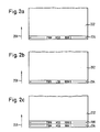
- Figures 2a-2c show a spatial light modulator array performing pulse width modulation and TDI at the beginning of a page.
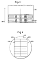
- Figure 3 shows a spatial light modulator array performing pulse width modulation and TDI in the middle of a page.
- Figure 4 shows a wafer with spatial light modulator arrays before they are separated into individual chips.
- FIGs 1a-1c show a prior art example of Time Delay and Integration (TDI) in computer to plate offset printing.
- the light rays impinge upon spatial light modulator 102.
- One cell shown in row 104 is activated, in this case shown as being deflected.
- Some examples of such modulators are Digital Micromirror Devices (DMD), Liquid Crystal Devices (LCD), and magneto-optic modulators.
- DMD Digital Micromirror Devices
- LCD Liquid Crystal Devices
- magneto-optic modulators magneto-optic modulators.
- the modulator shown is assumed to be a DMD, comprising an array of individual mirrors that are deflectable such as is shown in Figure 1a.
- Figure 1c shows another step in the process.
- the data that had been in row 106 in Figure 1b is now at row 114 in Figure 1c.
- the deflected element passes the light through the lens and again strikes the spot 112 on plate 110. This allows multiple time exposures of the same spot on the plate as it passes by the modulator, or as the modulator passes by the plate.
- Figures 2a-2c show a method that achieves a larger number of gray shades than simple time delay and integration (TDI).
- the printing process moves in the direction of arrow 208.
- the face of spatial light modulator is being viewed from what is seen as the vertical edge next to modulator row 104 in Figures 1a-1c.
- the modulator selected must have a relatively fast response time. For 600 dots-per-inch (dpi), the modulator has to load and display its data quickly. For example, assume a printer that prints 40 pages per minute, allowing 440 inches per minute, or 7.3 inches per sec. At 600 dpi, one inch has 600 pixels, requiring the modulator to print 4400 pixels per sec.
- the device configuration is assumed to be 2600 columns and 128 rows (600 dpi x 8.5" equals 5100 columns of pixels, so there are two devices of 2600 columns each). Worst case would be if the entire device 2600 x 128, or 332,800 pixels would have to be loaded at once. Printing 440 pixels per sec x 332,800, results in a 1.46 GHz data rate, a very difficult rate to achieve.
- the modulator would be divided into 58 blocks.
- the number of frames per page equals 600 dots/inch x 11.5 inch/page, or 6900 frames/page, and 6900 frames/page x pages/sec equals the frames per second.
- a highly competitive page rate would be 40 pages per minute, or 40/60 pages/sec. This results in a frame rate of 4600 frames per second.
- the resulting frame time equals 217 ⁇ secs per frame.
- a least significant bit (LSB) time of 217 ⁇ secs means that with no pulse-width modulation, the device would have to be loaded in 217 ⁇ secs.
- the LSB time would be divided by the number of bits of PWM. For example, if 2 bits of PWM is desired, the LSB time becomes 217 ⁇ secs/2, or 108 ⁇ secs. For faster modulators, this time presents no significant problems with loading the device.
- a 2-bit system by 128 TDI would provide 256 shades of gray.
- the modulator is shown at the very beginning of the cycle.
- the first row encountered in the process direction 204 displays the data for the most significant bit (MSB) for Row 0 of the printed image.
- row 204 on the modulator displays the LSB for the same row.
- Data line 0 then moves to the next row on the modulator in Figure 2c.
- the MSB for Row 0 is now on modulator row 206, and the MSB for Row 1 is on modulator row 204. This process continues up the device. Note that in this case there is no optical reversion as in Figures 1a-1c.
- Figure 3 shows an example later in time on a portion of modulator 302. The process still moves in direction of the arrow 308.
- Modulator row 306 is not modulating the data for the MSB of Row 63, and row 304 of the modulator displays the MSB of Row 64. The rest of the modulator's 128 rows would have the bottom 64 rows displaying Rows' 1-64 data onto the drum.
- FIG. 4 shows an illustration of this advantage at the wafer level.
- the wafer 402 has a set of modulators that are essentially finished except for the final dicing of the wafer.
- the modulators would be tested while on the wafer. If for example, modulators 404a and 406a both tested correctly, they could be left connected together and used in the PCB system, which requires high energy transfer. The two would essentially become a 2600 x 256 modulator array, in an embodiment where the modulators were 2600 x 128.
- modulators 404a and 404b would remain linked and go into a 600 dpi printing system. They would function as a 5200 x 128 array. They can still compete in the gray scale area because of the above technique, requiring fewer lines of a modulator for 256 shades of gray. In the above situation, where 406a is a inoperative modulator, and 404a and 404b stay linked for printing, modulator 406b appears to go to waste. However, because of the above techniques, it can still achieve 256 shades of gray, but at 300 dpi. The single modulators can be used in lower-end printing systems.
Landscapes
- Engineering & Computer Science (AREA)
- Multimedia (AREA)
- Signal Processing (AREA)
- Printers Or Recording Devices Using Electromagnetic And Radiation Means (AREA)
- Mechanical Light Control Or Optical Switches (AREA)
- Dot-Matrix Printers And Others (AREA)
- Color, Gradation (AREA)
- Exposure And Positioning Against Photoresist Photosensitive Materials (AREA)
Applications Claiming Priority (2)
| Application Number | Priority Date | Filing Date | Title |
|---|---|---|---|
| US38392 | 1993-03-29 | ||
| US08/038,392 US5455602A (en) | 1993-03-29 | 1993-03-29 | Combined modulation schemes for spatial light modulators |
Publications (2)
| Publication Number | Publication Date |
|---|---|
| EP0652669A1 true EP0652669A1 (de) | 1995-05-10 |
| EP0652669B1 EP0652669B1 (de) | 1999-10-20 |
Family
ID=21899685
Family Applications (1)
| Application Number | Title | Priority Date | Filing Date |
|---|---|---|---|
| EP94104496A Expired - Lifetime EP0652669B1 (de) | 1993-03-29 | 1994-03-22 | Schemata mit kombinierten Modulatoren für räumliche Lichtmodulatoren |
Country Status (7)
| Country | Link |
|---|---|
| US (1) | US5455602A (de) |
| EP (1) | EP0652669B1 (de) |
| JP (1) | JPH07125316A (de) |
| KR (1) | KR100324055B1 (de) |
| CN (1) | CN1049780C (de) |
| DE (1) | DE69421241T2 (de) |
| TW (1) | TW284934B (de) |
Cited By (1)
| Publication number | Priority date | Publication date | Assignee | Title |
|---|---|---|---|---|
| EP0795995A1 (de) * | 1996-03-14 | 1997-09-17 | Agfa-Gevaert N.V. | Halbtonreproduktion durch Aufzeichnung einzelner Punkte mittels mehrerer Laserstrahlen |
Families Citing this family (53)
| Publication number | Priority date | Publication date | Assignee | Title |
|---|---|---|---|---|
| US6219015B1 (en) | 1992-04-28 | 2001-04-17 | The Board Of Directors Of The Leland Stanford, Junior University | Method and apparatus for using an array of grating light valves to produce multicolor optical images |
| US5615016A (en) * | 1994-11-04 | 1997-03-25 | Texas Instruments Incorporated | Exposure scheme for minimizing microbanding inslm-based printers |
| US5841579A (en) | 1995-06-07 | 1998-11-24 | Silicon Light Machines | Flat diffraction grating light valve |
| DE19545625C1 (de) * | 1995-12-07 | 1997-11-13 | Agfa Gevaert Ag | Verfahren und Vorrichtung zur Aufzeichnung von Bildern mittels elektronischer Bildsignale |
| US6057809A (en) * | 1996-08-21 | 2000-05-02 | Neomagic Corp. | Modulation of line-select times of individual rows of a flat-panel display for gray-scaling |
| US5982553A (en) | 1997-03-20 | 1999-11-09 | Silicon Light Machines | Display device incorporating one-dimensional grating light-valve array |
| DE19733369A1 (de) * | 1997-08-01 | 1998-10-29 | Agfa Gevaert Ag | Verfahren und Vorrichtung zum Erzeugen eines Abbildes in einem Abbildungssystem |
| US6088102A (en) | 1997-10-31 | 2000-07-11 | Silicon Light Machines | Display apparatus including grating light-valve array and interferometric optical system |
| EP0933925A3 (de) | 1997-12-31 | 2002-06-26 | Texas Instruments Inc. | Fotobehandlung mit modulierten Lichtquellengittern |
| US6271808B1 (en) | 1998-06-05 | 2001-08-07 | Silicon Light Machines | Stereo head mounted display using a single display device |
| US6130770A (en) | 1998-06-23 | 2000-10-10 | Silicon Light Machines | Electron gun activated grating light valve |
| US6101036A (en) | 1998-06-23 | 2000-08-08 | Silicon Light Machines | Embossed diffraction grating alone and in combination with changeable image display |
| US6215579B1 (en) | 1998-06-24 | 2001-04-10 | Silicon Light Machines | Method and apparatus for modulating an incident light beam for forming a two-dimensional image |
| US6303986B1 (en) | 1998-07-29 | 2001-10-16 | Silicon Light Machines | Method of and apparatus for sealing an hermetic lid to a semiconductor die |
| US6872984B1 (en) | 1998-07-29 | 2005-03-29 | Silicon Light Machines Corporation | Method of sealing a hermetic lid to a semiconductor die at an angle |
| US6414706B1 (en) | 1998-10-30 | 2002-07-02 | Texas Instruments Incorporated | High resolution digital printing with spatial light modulator |
| US6956878B1 (en) | 2000-02-07 | 2005-10-18 | Silicon Light Machines Corporation | Method and apparatus for reducing laser speckle using polarization averaging |
| US7177081B2 (en) | 2001-03-08 | 2007-02-13 | Silicon Light Machines Corporation | High contrast grating light valve type device |
| US6707591B2 (en) | 2001-04-10 | 2004-03-16 | Silicon Light Machines | Angled illumination for a single order light modulator based projection system |
| US6865346B1 (en) | 2001-06-05 | 2005-03-08 | Silicon Light Machines Corporation | Fiber optic transceiver |
| US6782205B2 (en) | 2001-06-25 | 2004-08-24 | Silicon Light Machines | Method and apparatus for dynamic equalization in wavelength division multiplexing |
| US6747781B2 (en) | 2001-06-25 | 2004-06-08 | Silicon Light Machines, Inc. | Method, apparatus, and diffuser for reducing laser speckle |
| JP3620477B2 (ja) | 2001-07-04 | 2005-02-16 | ヤマハ株式会社 | 信号情報表示装置 |
| US6829092B2 (en) | 2001-08-15 | 2004-12-07 | Silicon Light Machines, Inc. | Blazed grating light valve |
| US6930364B2 (en) | 2001-09-13 | 2005-08-16 | Silicon Light Machines Corporation | Microelectronic mechanical system and methods |
| US6956995B1 (en) | 2001-11-09 | 2005-10-18 | Silicon Light Machines Corporation | Optical communication arrangement |
| US6800238B1 (en) | 2002-01-15 | 2004-10-05 | Silicon Light Machines, Inc. | Method for domain patterning in low coercive field ferroelectrics |
| US6767751B2 (en) | 2002-05-28 | 2004-07-27 | Silicon Light Machines, Inc. | Integrated driver process flow |
| US6728023B1 (en) | 2002-05-28 | 2004-04-27 | Silicon Light Machines | Optical device arrays with optimized image resolution |
| US7054515B1 (en) | 2002-05-30 | 2006-05-30 | Silicon Light Machines Corporation | Diffractive light modulator-based dynamic equalizer with integrated spectral monitor |
| US6822797B1 (en) | 2002-05-31 | 2004-11-23 | Silicon Light Machines, Inc. | Light modulator structure for producing high-contrast operation using zero-order light |
| US6829258B1 (en) | 2002-06-26 | 2004-12-07 | Silicon Light Machines, Inc. | Rapidly tunable external cavity laser |
| US6813059B2 (en) | 2002-06-28 | 2004-11-02 | Silicon Light Machines, Inc. | Reduced formation of asperities in contact micro-structures |
| US6908201B2 (en) | 2002-06-28 | 2005-06-21 | Silicon Light Machines Corporation | Micro-support structures |
| US6801354B1 (en) | 2002-08-20 | 2004-10-05 | Silicon Light Machines, Inc. | 2-D diffraction grating for substantially eliminating polarization dependent losses |
| US7057795B2 (en) | 2002-08-20 | 2006-06-06 | Silicon Light Machines Corporation | Micro-structures with individually addressable ribbon pairs |
| CN101487982A (zh) * | 2002-08-24 | 2009-07-22 | 无掩模平版印刷公司 | 连续地直接写的光刻技术 |
| US6712480B1 (en) | 2002-09-27 | 2004-03-30 | Silicon Light Machines | Controlled curvature of stressed micro-structures |
| US6928207B1 (en) | 2002-12-12 | 2005-08-09 | Silicon Light Machines Corporation | Apparatus for selectively blocking WDM channels |
| US7057819B1 (en) | 2002-12-17 | 2006-06-06 | Silicon Light Machines Corporation | High contrast tilting ribbon blazed grating |
| US6987600B1 (en) | 2002-12-17 | 2006-01-17 | Silicon Light Machines Corporation | Arbitrary phase profile for better equalization in dynamic gain equalizer |
| US6934070B1 (en) | 2002-12-18 | 2005-08-23 | Silicon Light Machines Corporation | Chirped optical MEM device |
| US6927891B1 (en) | 2002-12-23 | 2005-08-09 | Silicon Light Machines Corporation | Tilt-able grating plane for improved crosstalk in 1×N blaze switches |
| US7068372B1 (en) | 2003-01-28 | 2006-06-27 | Silicon Light Machines Corporation | MEMS interferometer-based reconfigurable optical add-and-drop multiplexor |
| US7286764B1 (en) | 2003-02-03 | 2007-10-23 | Silicon Light Machines Corporation | Reconfigurable modulator-based optical add-and-drop multiplexer |
| US6947613B1 (en) | 2003-02-11 | 2005-09-20 | Silicon Light Machines Corporation | Wavelength selective switch and equalizer |
| US6922272B1 (en) | 2003-02-14 | 2005-07-26 | Silicon Light Machines Corporation | Method and apparatus for leveling thermal stress variations in multi-layer MEMS devices |
| US6829077B1 (en) | 2003-02-28 | 2004-12-07 | Silicon Light Machines, Inc. | Diffractive light modulator with dynamically rotatable diffraction plane |
| US7391973B1 (en) | 2003-02-28 | 2008-06-24 | Silicon Light Machines Corporation | Two-stage gain equalizer |
| US7027202B1 (en) | 2003-02-28 | 2006-04-11 | Silicon Light Machines Corp | Silicon substrate as a light modulator sacrificial layer |
| US6922273B1 (en) | 2003-02-28 | 2005-07-26 | Silicon Light Machines Corporation | PDL mitigation structure for diffractive MEMS and gratings |
| US6806997B1 (en) | 2003-02-28 | 2004-10-19 | Silicon Light Machines, Inc. | Patterned diffractive light modulator ribbon for PDL reduction |
| US7042611B1 (en) | 2003-03-03 | 2006-05-09 | Silicon Light Machines Corporation | Pre-deflected bias ribbons |
Citations (4)
| Publication number | Priority date | Publication date | Assignee | Title |
|---|---|---|---|---|
| US4074319A (en) * | 1976-12-13 | 1978-02-14 | Bell Telephone Laboratories, Incorporated | Light emitting diode array imaging system - parallel approach |
| EP0321143A2 (de) * | 1987-12-17 | 1989-06-21 | AT&T Corp. | Verfahren und Gerät zum direkten Farbdruck |
| US5061049A (en) * | 1984-08-31 | 1991-10-29 | Texas Instruments Incorporated | Spatial light modulator and method |
| EP0467048A2 (de) * | 1990-06-29 | 1992-01-22 | Texas Instruments Incorporated | Deformierbare Spiegelvorrichtung mit aktualisiertem Raster |
Family Cites Families (5)
| Publication number | Priority date | Publication date | Assignee | Title |
|---|---|---|---|---|
| US4054797A (en) * | 1976-09-23 | 1977-10-18 | The United States Of America As Represented By The Secretary Of The Navy | Series-parallel scan, IR, CID, focal-plane array |
| US4638309A (en) * | 1983-09-08 | 1987-01-20 | Texas Instruments Incorporated | Spatial light modulator drive system |
| US5132773A (en) * | 1991-02-06 | 1992-07-21 | Olin Corporation | Carrier ring having first and second ring means with bonded surfaces |
| US5280280A (en) * | 1991-05-24 | 1994-01-18 | Robert Hotto | DC integrating display driver employing pixel status memories |
| US5357273A (en) * | 1991-07-29 | 1994-10-18 | Xerox Corporation | Resolution conversion via intensity controlled overscanned illumination for optical printers and the like having high gamma photosensitive recording media |
-
1993
- 1993-03-29 US US08/038,392 patent/US5455602A/en not_active Expired - Lifetime
-
1994
- 1994-03-22 EP EP94104496A patent/EP0652669B1/de not_active Expired - Lifetime
- 1994-03-22 DE DE69421241T patent/DE69421241T2/de not_active Expired - Fee Related
- 1994-03-28 KR KR1019940006205A patent/KR100324055B1/ko not_active Expired - Fee Related
- 1994-03-28 JP JP6057655A patent/JPH07125316A/ja active Pending
- 1994-03-29 CN CN94103177A patent/CN1049780C/zh not_active Expired - Fee Related
- 1994-08-22 TW TW083107652A patent/TW284934B/zh active
Patent Citations (4)
| Publication number | Priority date | Publication date | Assignee | Title |
|---|---|---|---|---|
| US4074319A (en) * | 1976-12-13 | 1978-02-14 | Bell Telephone Laboratories, Incorporated | Light emitting diode array imaging system - parallel approach |
| US5061049A (en) * | 1984-08-31 | 1991-10-29 | Texas Instruments Incorporated | Spatial light modulator and method |
| EP0321143A2 (de) * | 1987-12-17 | 1989-06-21 | AT&T Corp. | Verfahren und Gerät zum direkten Farbdruck |
| EP0467048A2 (de) * | 1990-06-29 | 1992-01-22 | Texas Instruments Incorporated | Deformierbare Spiegelvorrichtung mit aktualisiertem Raster |
Cited By (1)
| Publication number | Priority date | Publication date | Assignee | Title |
|---|---|---|---|---|
| EP0795995A1 (de) * | 1996-03-14 | 1997-09-17 | Agfa-Gevaert N.V. | Halbtonreproduktion durch Aufzeichnung einzelner Punkte mittels mehrerer Laserstrahlen |
Also Published As
| Publication number | Publication date |
|---|---|
| JPH07125316A (ja) | 1995-05-16 |
| DE69421241D1 (de) | 1999-11-25 |
| DE69421241T2 (de) | 2000-05-11 |
| CN1049780C (zh) | 2000-02-23 |
| TW284934B (de) | 1996-09-01 |
| KR100324055B1 (ko) | 2002-07-08 |
| EP0652669B1 (de) | 1999-10-20 |
| US5455602A (en) | 1995-10-03 |
| CN1101433A (zh) | 1995-04-12 |
Similar Documents
| Publication | Publication Date | Title |
|---|---|---|
| US5455602A (en) | Combined modulation schemes for spatial light modulators | |
| CN1055588C (zh) | 数字微反射器印刷机的方法和构造 | |
| US5696549A (en) | Method of reducing print artifacts | |
| US5461410A (en) | Gray scale printing using spatial light modulators | |
| US5953103A (en) | Color printer | |
| EP0689181A1 (de) | Speicherschaltungen für räumliche Lichtmodulatoren | |
| EP0321143B1 (de) | Verfahren und Gerät zum direkten Farbdruck | |
| US6295078B1 (en) | Methods of providing lower resolution format data into a higher resolution format | |
| US5166999A (en) | High resolution print bar system | |
| EP0713192B1 (de) | Druckverfahren und Drucker unter Verwendung eines räumlichen Modulators | |
| US5043743A (en) | Method and apparatus for the image-wise exposure of light-sensitive medium by a plurality of light valves | |
| JPH09265139A (ja) | 画像露光装置および画像表示装置 | |
| US5140350A (en) | Image forming apparatus for forming an image with smooth curved lines | |
| KR100379731B1 (ko) | Slm이용프린터에서마이크로밴딩을최소화하는노광방법에의한프린팅방법 | |
| KR100189853B1 (ko) | 전자사진 화상형성장치 | |
| JPS63280665A (ja) | 液晶プリンタヘッド | |
| JPH05286173A (ja) | 強誘電性液晶シャッターヘッド | |
| JPH0852899A (ja) | 高解像度プリント方法および空間光変調器アレイ | |
| Banks et al. | Digital ferroelectric printhead technology | |
| JPS63280278A (ja) | 液晶プリンタヘッド | |
| JPH09318893A (ja) | プリント画像の欠陥画素修復方法及び写真プリンタ |
Legal Events
| Date | Code | Title | Description |
|---|---|---|---|
| PUAI | Public reference made under article 153(3) epc to a published international application that has entered the european phase |
Free format text: ORIGINAL CODE: 0009012 |
|
| AK | Designated contracting states |
Kind code of ref document: A1 Designated state(s): DE FR GB IT NL |
|
| 17P | Request for examination filed |
Effective date: 19951026 |
|
| 17Q | First examination report despatched |
Effective date: 19971110 |
|
| GRAG | Despatch of communication of intention to grant |
Free format text: ORIGINAL CODE: EPIDOS AGRA |
|
| GRAG | Despatch of communication of intention to grant |
Free format text: ORIGINAL CODE: EPIDOS AGRA |
|
| GRAH | Despatch of communication of intention to grant a patent |
Free format text: ORIGINAL CODE: EPIDOS IGRA |
|
| GRAH | Despatch of communication of intention to grant a patent |
Free format text: ORIGINAL CODE: EPIDOS IGRA |
|
| GRAA | (expected) grant |
Free format text: ORIGINAL CODE: 0009210 |
|
| AK | Designated contracting states |
Kind code of ref document: B1 Designated state(s): DE FR GB IT NL |
|
| PG25 | Lapsed in a contracting state [announced via postgrant information from national office to epo] |
Ref country code: IT Free format text: LAPSE BECAUSE OF FAILURE TO SUBMIT A TRANSLATION OF THE DESCRIPTION OR TO PAY THE FEE WITHIN THE PRESCRIBED TIME-LIMIT;WARNING: LAPSES OF ITALIAN PATENTS WITH EFFECTIVE DATE BEFORE 2007 MAY HAVE OCCURRED AT ANY TIME BEFORE 2007. THE CORRECT EFFECTIVE DATE MAY BE DIFFERENT FROM THE ONE RECORDED. Effective date: 19991020 |
|
| ET | Fr: translation filed | ||
| REF | Corresponds to: |
Ref document number: 69421241 Country of ref document: DE Date of ref document: 19991125 |
|
| PGFP | Annual fee paid to national office [announced via postgrant information from national office to epo] |
Ref country code: NL Payment date: 20000313 Year of fee payment: 7 |
|
| PLBE | No opposition filed within time limit |
Free format text: ORIGINAL CODE: 0009261 |
|
| STAA | Information on the status of an ep patent application or granted ep patent |
Free format text: STATUS: NO OPPOSITION FILED WITHIN TIME LIMIT |
|
| 26N | No opposition filed | ||
| PGFP | Annual fee paid to national office [announced via postgrant information from national office to epo] |
Ref country code: FR Payment date: 20010822 Year of fee payment: 8 |
|
| PG25 | Lapsed in a contracting state [announced via postgrant information from national office to epo] |
Ref country code: NL Free format text: LAPSE BECAUSE OF NON-PAYMENT OF DUE FEES Effective date: 20011001 |
|
| NLV4 | Nl: lapsed or anulled due to non-payment of the annual fee |
Effective date: 20011001 |
|
| REG | Reference to a national code |
Ref country code: GB Ref legal event code: IF02 |
|
| PG25 | Lapsed in a contracting state [announced via postgrant information from national office to epo] |
Ref country code: FR Free format text: LAPSE BECAUSE OF NON-PAYMENT OF DUE FEES Effective date: 20021129 |
|
| REG | Reference to a national code |
Ref country code: FR Ref legal event code: ST |
|
| PGFP | Annual fee paid to national office [announced via postgrant information from national office to epo] |
Ref country code: GB Payment date: 20080211 Year of fee payment: 15 |
|
| PGFP | Annual fee paid to national office [announced via postgrant information from national office to epo] |
Ref country code: DE Payment date: 20080331 Year of fee payment: 15 |
|
| GBPC | Gb: european patent ceased through non-payment of renewal fee |
Effective date: 20090322 |
|
| PG25 | Lapsed in a contracting state [announced via postgrant information from national office to epo] |
Ref country code: DE Free format text: LAPSE BECAUSE OF NON-PAYMENT OF DUE FEES Effective date: 20091001 |
|
| PG25 | Lapsed in a contracting state [announced via postgrant information from national office to epo] |
Ref country code: GB Free format text: LAPSE BECAUSE OF NON-PAYMENT OF DUE FEES Effective date: 20090322 |