EP0653111B1 - Protection contre les inversions de polarite a l'aide d'un element de protection a surface reduite - Google Patents
Protection contre les inversions de polarite a l'aide d'un element de protection a surface reduite Download PDFInfo
- Publication number
- EP0653111B1 EP0653111B1 EP93915646A EP93915646A EP0653111B1 EP 0653111 B1 EP0653111 B1 EP 0653111B1 EP 93915646 A EP93915646 A EP 93915646A EP 93915646 A EP93915646 A EP 93915646A EP 0653111 B1 EP0653111 B1 EP 0653111B1
- Authority
- EP
- European Patent Office
- Prior art keywords
- polarity
- reversal protection
- current
- protection element
- conductor system
- Prior art date
- Legal status (The legal status is an assumption and is not a legal conclusion. Google has not performed a legal analysis and makes no representation as to the accuracy of the status listed.)
- Expired - Lifetime
Links
- 239000004020 conductor Substances 0.000 claims abstract description 24
- 230000008878 coupling Effects 0.000 claims abstract description 23
- 238000010168 coupling process Methods 0.000 claims abstract description 23
- 238000005859 coupling reaction Methods 0.000 claims abstract description 23
- 238000004804 winding Methods 0.000 claims abstract description 20
- 239000003990 capacitor Substances 0.000 claims description 9
- 230000005540 biological transmission Effects 0.000 description 23
- 230000010365 information processing Effects 0.000 description 2
- XUIMIQQOPSSXEZ-UHFFFAOYSA-N Silicon Chemical compound [Si] XUIMIQQOPSSXEZ-UHFFFAOYSA-N 0.000 description 1
- 238000006243 chemical reaction Methods 0.000 description 1
- 230000000694 effects Effects 0.000 description 1
- 230000001939 inductive effect Effects 0.000 description 1
- 230000010354 integration Effects 0.000 description 1
- 239000000463 material Substances 0.000 description 1
- 239000004065 semiconductor Substances 0.000 description 1
- 229910052710 silicon Inorganic materials 0.000 description 1
- 239000010703 silicon Substances 0.000 description 1
Images

Classifications
-
- H—ELECTRICITY
- H02—GENERATION; CONVERSION OR DISTRIBUTION OF ELECTRIC POWER
- H02H—EMERGENCY PROTECTIVE CIRCUIT ARRANGEMENTS
- H02H11/00—Emergency protective circuit arrangements for preventing the switching-on in case an undesired electric working condition might result
- H02H11/002—Emergency protective circuit arrangements for preventing the switching-on in case an undesired electric working condition might result in case of inverted polarity or connection; with switching for obtaining correct connection
-
- H—ELECTRICITY
- H04—ELECTRIC COMMUNICATION TECHNIQUE
- H04B—TRANSMISSION
- H04B3/00—Line transmission systems
- H04B3/54—Systems for transmission via power distribution lines
- H04B3/548—Systems for transmission via power distribution lines the power on the line being DC
-
- H—ELECTRICITY
- H04—ELECTRIC COMMUNICATION TECHNIQUE
- H04B—TRANSMISSION
- H04B2203/00—Indexing scheme relating to line transmission systems
- H04B2203/54—Aspects of powerline communications not already covered by H04B3/54 and its subgroups
- H04B2203/5462—Systems for power line communications
- H04B2203/547—Systems for power line communications via DC power distribution
-
- H—ELECTRICITY
- H04—ELECTRIC COMMUNICATION TECHNIQUE
- H04B—TRANSMISSION
- H04B2203/00—Indexing scheme relating to line transmission systems
- H04B2203/54—Aspects of powerline communications not already covered by H04B3/54 and its subgroups
- H04B2203/5462—Systems for power line communications
- H04B2203/5483—Systems for power line communications using coupling circuits
Definitions
- the invention relates to reverse polarity protection for coupling an electrical circuit to an energy and information-carrying conductor system, at least one coupling path comprising a controllable element as reverse polarity protection.
- Such reverse polarity protection is known (EP-A-0 487 759).
- the reverse polarity protection element requires a relatively large element area, that is to say a correspondingly large silicon area in the case of conventional semiconductor material.
- the invention has for its object to improve the known reverse polarity protection so that the element surface can be significantly reduced in the reverse polarity protection element.
- the reverse polarity protection element can be extended up to a gain B of, for example, three.
- the gain is defined as the quotient from the collector current to the base current.
- the reverse polarity protection can be used to couple an electrical circuit to a conductor system carrying direct current energy and alternating voltage information.
- at least one coupling path comprises a controllable element as reverse polarity protection, for which purpose this reverse polarity protection element blocks or enables the coupling path depending on the polarity of the conductor system. It is essential that when a transmitter circuit is inductively coupled to the conductor system by a converter which, in conjunction with a capacitor, serves as a switch for direct current energy and for alternating voltage information, the working current of the winding of the converter serving as the transmitter winding is conducted via the control electrode of the controllable element.
- the capacitor is arranged in the line, in the train of which there is a working electrode, for example the emitter, of the polarity reversal protection element.
- a line for the signal current of the transmitter is led to the control electrode of the reverse polarity protection element.
- the working current via the winding on the transmitter side is also conducted here via the control electrode of the reverse polarity protection element.
- the capacitor lies between energy-carrying lines.
- the polarity reversal protection element is designed as a symmetrical double emitter transistor, the control input of which is connected to a control circuit in addition to the line for the transmission current.
- a double-emitter transistor with the appropriate wiring on the transmitter side, enables an energy freewheeling in the pauses of the transmission signal, without further wiring on the reverse polarity protection element.
- Such a double emitter transistor can advantageously be used for a variety of circuit-related tasks. Such designs are particularly suitable for integration in an IC.
- a reverse polarity protection is illustrated in FIG.
- the reverse polarity protection element 4 ensures that the coupling path 5 is blocked or released depending on the polarity of the conductor system 3.
- the circuit 2 can be understood as a transmission circuit which is inductively coupled to the conductor system 3 by a converter 6.
- the converter 6 serves as a switch for direct current energy and for alternating voltage information, which are transmitted via the conductor system 3.
- the transmission current is conducted via the primary side 7 of the converter 6.
- the secondary windings 8 facing the conductor system 3 allow direct current energy to be taken from the capacitor 11 of the coupling circuit 1 on both sides of the capacitor 11. If the reverse polarity protection element 4 when connecting the coupling circuit 1 to the conductor system 3 as a result of incorrect connection direction and correspondingly incorrect polarity, the on-board electrical system supply and thus the coupling circuit are not operated without short-circuiting effects occurring for the conductor system 3. The conductor system 3 is therefore not loaded when a coupling circuit is connected in the wrong way.
- the polarity reversal protection element 4 consists of a transistor 9 and a parallel valve 10, which can also be formed by a second transistor connected in anti-parallel.
- the transmission power is controlled by a transmission valve 12.
- the operating current of the transmission valve 12 is conducted via a further coupling path 18 to the control electrode of the reverse polarity protection element.
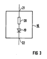
- a control circuit 16 also works on this control electrode.
- the control circuit 16 is designed in such a way that it supplies the polarity reversal protection element 4 with a corresponding control current, depending on the operating state, for example receiving or transmitting, or high direct current requirements for the vehicle electrical system. It is assumed that a current of a few milliamperes flows through the polarity reversal protection element 4, for example of 10 milliamperes, in the normal receiving operating state. A current in the order of magnitude of, for example, + 0.3 amperes then flows during transmission operation. This requires a considerably larger control current for the polarity reversal protection element 4.
- the working current flowing through the winding 7 on the transmitter side is conducted via the control electrode of the reverse polarity protection element and the greater control current is thus applied.
- the base of a symmetrical double emitter (symmetrical bi-polar transistor) transistor serves as the control electrode.
- the control circuit 16 is designed such that, with correct polarity, the reverse polarity protection element is turned on by drawing current from the base of the polarity reversal protection element 4. If the polarity is incorrect, that is to say if the transmission circuit 2 is connected with the wrong polarity, the control circuit 16 does not draw any current, that is to say it blocks, so that the polarity reversal protection element 4 is not conductively controlled, that is to say it blocks. Furthermore, it is therefore designed such that the required control current is provided in each case during transmission operation or when the connected circuit, including the transmission circuit 2, requires more power.
- the commutation current is used as a control current.
- a control unit of the type of the control circuit 16 has a control inertia, so that a high-impedance intermediate state occurs before positive or negative current through the controlled element.
- This disadvantage is avoided by redirecting the commutation current according to the invention and using it as a control current, which is guided over the base of the polarity reversal protection element 4, which can be regarded here as an element to be controlled.
- the commutation current as an additional control current, one avoids the high-resistance intermediate state. This enables you to control the system without inertia.
- a symmetrical double emitter transistor is therefore to be understood to mean a symmetrical structure, for example of a pnp bipolar transistor, in which, depending on the current direction, one of the emitters becomes a collector. In relation to a normal transistor with emitter and collector, the current flows in normal operation and then in inverse operation.
- the polarity reversal protection element 4 is designed as a double emitter transistor, as is illustrated in FIG. 2.
- the working current from the transmission valve 12 via the transmission winding or primary winding 7 is again passed through the control electrode of the polarity reversal protection element 4.
- a symmetrical transmission mode is made possible by two transmission valves 12 and 13.
- the operating current of the transmission valve 12 is fed to the control electrode of the polarity reversal protection element 4 via a further coupling path 18 - as in FIG. 1.
- Two valves 14 and 15 are arranged in a branch parallel to the capacitor 11, in which the winding 7 lies on the information processing side.
- the winding 7 is arranged between these valves.
- valves 14 and 15 the coil 7 is switched in phase opposition with respect to the transmission valves 12 and 13 in the transmission branch.
- the valves 14 and 15 provide a type of free-wheeling circuit for the primary winding or transmission winding 7 in the pauses of the transmission pulses, but of a special type, as described in detail in EP-A-0 379 902.
- the energy stored in the winding on the information processing side is thereby recovered and brought to the energy-feeding secondary side of the converter.
- the efficiency of the system is increased in a bus system as a conductor system 3 with many coupling circuits.
Landscapes
- Engineering & Computer Science (AREA)
- Power Engineering (AREA)
- Computer Networks & Wireless Communication (AREA)
- Signal Processing (AREA)
- Emergency Protection Circuit Devices (AREA)
- Semiconductor Integrated Circuits (AREA)
- Charge And Discharge Circuits For Batteries Or The Like (AREA)
- Facsimile Transmission Control (AREA)
- Bipolar Transistors (AREA)
- Power Conversion In General (AREA)
Claims (3)
- Protection contre l'inversion de pôles, destinée au couplage d'un circuit électrique (2) à un système (3) de conducteurs véhiculant de l'énergie et de l'information, au moins une voie (5) de couplage comprenant comme protection contre l'inversion de pôles un élément (4) pouvant être commandé, caractérisée qu'en cas de couplage inductif d'un circuit (2) d'émission au système (3) de conducteurs au moyen d'un transformateur (6), le courant de fonctionnement, qui passe par l'enroulement (7) du côté émission, conduit par l'intermédiaire de l'électrode de commande de l'élément pouvant être commandé, appelé élément (4) de protection contre l'inversion des pôles.
- Protection contre l'inversion de pôles, destinée au couplage d'un circuit électrique (2) à un système (3) de conducteurs véhiculant une énergie en courant continu et une information de tension alternative, au moins une branche (5) de couplage comprenant comme protection contre l'inversion de pôles un élément (4) pouvant être commandé, cet élément (4) de protection contre l'inversion des pôles bloquant ou libérant, en fonction de la polarité du système (3) de conducteurs, la voie (5) de couplage, caractérisée en ce qu'en cas de couplage inductif du circuit (2) d'émission au système (3) de conducteurs par un transformateur (6), qui sert, en liaison avec un condensateur (11) d'aiguillage de l'énergie en courant continu et de l'information en tension alternative, le courant de fonctionnement, qui passe par l'enroulement du transformateur (6) servant d'enroulement (7) d'émission, est conduit par l'intermédiaire de l'électrode de commande de l'élément (4) de protection contre l'inversion des pôles, par le fait que le condensateur (11) est disposé dans une ligne, à la suite de laquelle se trouve une électrode de fonctionnement, par exemple l'émetteur, de l'élément (4) de protection contre l'inversion des pôles, et une autre voie (18) de couplage du courant d'émission est amenée à l'électrode de commande de l'élément (4) de protection contre l'inversion de pôles.
- Protection contre l'inversion de pôles suivant la revendication 1 ou 2, caractérisée en ce que l'élément (4) de protection contre l'inversion de pôles est un transistor (17) symétrique à émetteur double, dont l'entrée de commande est reliée, outre à la ligne pour le courant d'émission, à un circuit (18) de commande.
Applications Claiming Priority (3)
| Application Number | Priority Date | Filing Date | Title |
|---|---|---|---|
| DE4225457 | 1992-07-31 | ||
| DE4225457 | 1992-07-31 | ||
| PCT/DE1993/000639 WO1994003956A1 (fr) | 1992-07-31 | 1993-07-20 | Protection contre les inversions de polarite a l'aide d'un element de protection a surface reduite |
Publications (2)
| Publication Number | Publication Date |
|---|---|
| EP0653111A1 EP0653111A1 (fr) | 1995-05-17 |
| EP0653111B1 true EP0653111B1 (fr) | 1996-09-18 |
Family
ID=6464634
Family Applications (1)
| Application Number | Title | Priority Date | Filing Date |
|---|---|---|---|
| EP93915646A Expired - Lifetime EP0653111B1 (fr) | 1992-07-31 | 1993-07-20 | Protection contre les inversions de polarite a l'aide d'un element de protection a surface reduite |
Country Status (6)
| Country | Link |
|---|---|
| EP (1) | EP0653111B1 (fr) |
| JP (1) | JPH07509834A (fr) |
| AT (1) | ATE143190T1 (fr) |
| AU (1) | AU669726B2 (fr) |
| DE (1) | DE59303897D1 (fr) |
| WO (1) | WO1994003956A1 (fr) |
Family Cites Families (2)
| Publication number | Priority date | Publication date | Assignee | Title |
|---|---|---|---|---|
| EP0379902B1 (fr) * | 1989-01-27 | 1994-09-07 | Siemens Aktiengesellschaft | Dispositif de traitement d'informations à couplage inductif |
| EP0487759B1 (fr) * | 1990-11-26 | 1995-04-26 | Siemens Aktiengesellschaft | Protection contre l'inversion des bornes de la batterie |
-
1993
- 1993-07-20 EP EP93915646A patent/EP0653111B1/fr not_active Expired - Lifetime
- 1993-07-20 JP JP6504884A patent/JPH07509834A/ja active Pending
- 1993-07-20 AU AU45577/93A patent/AU669726B2/en not_active Ceased
- 1993-07-20 DE DE59303897T patent/DE59303897D1/de not_active Expired - Fee Related
- 1993-07-20 WO PCT/DE1993/000639 patent/WO1994003956A1/fr not_active Ceased
- 1993-07-20 AT AT93915646T patent/ATE143190T1/de not_active IP Right Cessation
Also Published As
| Publication number | Publication date |
|---|---|
| EP0653111A1 (fr) | 1995-05-17 |
| DE59303897D1 (de) | 1996-10-24 |
| WO1994003956A1 (fr) | 1994-02-17 |
| JPH07509834A (ja) | 1995-10-26 |
| AU4557793A (en) | 1994-03-03 |
| ATE143190T1 (de) | 1996-10-15 |
| AU669726B2 (en) | 1996-06-20 |
Similar Documents
| Publication | Publication Date | Title |
|---|---|---|
| DE1171983B (de) | Selbstgesteuerter Wechselrichter mit Transistoren | |
| DE3231788C2 (de) | Ansteuerschaltung für elektronische Leistungsschalter | |
| DE3618221C1 (de) | Schaltnetzteil mit einem primaer getakteten Gleichspannungswandler | |
| DE2342294B2 (de) | Schaltungsanordnung zur galvanischen Trennung von analogen Gleichstromsignalen | |
| DE2255220B2 (de) | Kontaktloser ueberlastschalter | |
| WO1994003956A1 (fr) | Protection contre les inversions de polarite a l'aide d'un element de protection a surface reduite | |
| EP0201700A1 (fr) | Commande pour enclencher et déclencher des composants semi-conducteurs de puissance | |
| DE2555260B2 (de) | Treiberschaltung zur Umsetzung der Übergänge eines nichtsymmetrischen Datencode in eine Folge abwechselnd positiver und negativer, je einen Übergang anzeigender Impulse | |
| EP0653110B1 (fr) | Protection contre les inversions de polarite avec element a surface reduite | |
| DE2647958C3 (de) | Schaltungsanordnung für einen fremdgesteuerten· Wechselrichter | |
| EP0048490B1 (fr) | Circuit pour transformer un signal d'entrée binaire en un signal télégraphique | |
| EP0949737A2 (fr) | Circuit de protection contre l'inversion des bornes de la batterie | |
| DE2422501A1 (de) | Schaltungsanordnung zur drehzahlstellung von gleichstrommotoren | |
| DE2132616A1 (de) | Tastschaltung fuer die abgabe von fernschreibzeichen mit konstantem ausgangsstrom | |
| DE2124390B2 (de) | Einrichtung zur Energieversorgung | |
| EP0487759B1 (fr) | Protection contre l'inversion des bornes de la batterie | |
| DE1275198B (de) | Transistorbrueckenwechselrichter | |
| EP0840433B1 (fr) | Alimentation de tension pour le circuit de commande d'un commutateur dans un convertisseur avec circuit intermédiaire de tension | |
| EP1398877B1 (fr) | Procédé pour détecter des erreurs dans une transmission d'informations à un circuit d'attaque | |
| DE102022119531A1 (de) | Stromrichtereinrichtung mit einem Stromrichter und mit einer Steuereinrichtung | |
| DE1226141B (de) | Schaltungsanordnung zur kontaktlosen Signaluebertragung von einem elektronischen Fernschreibsender auf die Leitung | |
| DE1939276C3 (de) | Steuerschaltung für einen Transistor-Wechselrichter in Gegentaktschaltung | |
| DE2408381B2 (de) | Schaltungsanordnung zur pulsbreitenmodulierten Ansteuerung von Leistungstransistoren | |
| DE1267339B (de) | Anordnung zur Lastumschaltung bei Stufentransformatoren mit steuerbaren Halbleitergleichrichtern | |
| DE1034263B (de) | Schaltungsanordnung fuer Kontaktumformer mit Schaltdrosselspulen |
Legal Events
| Date | Code | Title | Description |
|---|---|---|---|
| PUAI | Public reference made under article 153(3) epc to a published international application that has entered the european phase |
Free format text: ORIGINAL CODE: 0009012 |
|
| 17P | Request for examination filed |
Effective date: 19941118 |
|
| AK | Designated contracting states |
Kind code of ref document: A1 Designated state(s): AT CH DE FR GB IT LI |
|
| 17Q | First examination report despatched |
Effective date: 19951010 |
|
| GRAH | Despatch of communication of intention to grant a patent |
Free format text: ORIGINAL CODE: EPIDOS IGRA |
|
| GRAH | Despatch of communication of intention to grant a patent |
Free format text: ORIGINAL CODE: EPIDOS IGRA |
|
| GRAA | (expected) grant |
Free format text: ORIGINAL CODE: 0009210 |
|
| AK | Designated contracting states |
Kind code of ref document: B1 Designated state(s): AT CH DE FR GB IT LI |
|
| REF | Corresponds to: |
Ref document number: 143190 Country of ref document: AT Date of ref document: 19961015 Kind code of ref document: T |
|
| REG | Reference to a national code |
Ref country code: CH Ref legal event code: NV Representative=s name: SIEMENS SCHWEIZ AG |
|
| REF | Corresponds to: |
Ref document number: 59303897 Country of ref document: DE Date of ref document: 19961024 |
|
| GBT | Gb: translation of ep patent filed (gb section 77(6)(a)/1977) |
Effective date: 19961025 |
|
| ITF | It: translation for a ep patent filed | ||
| ET | Fr: translation filed | ||
| PLBE | No opposition filed within time limit |
Free format text: ORIGINAL CODE: 0009261 |
|
| STAA | Information on the status of an ep patent application or granted ep patent |
Free format text: STATUS: NO OPPOSITION FILED WITHIN TIME LIMIT |
|
| 26N | No opposition filed | ||
| REG | Reference to a national code |
Ref country code: GB Ref legal event code: IF02 |
|
| PGFP | Annual fee paid to national office [announced via postgrant information from national office to epo] |
Ref country code: GB Payment date: 20030710 Year of fee payment: 11 |
|
| PGFP | Annual fee paid to national office [announced via postgrant information from national office to epo] |
Ref country code: AT Payment date: 20040623 Year of fee payment: 12 |
|
| PGFP | Annual fee paid to national office [announced via postgrant information from national office to epo] |
Ref country code: FR Payment date: 20040716 Year of fee payment: 12 |
|
| PG25 | Lapsed in a contracting state [announced via postgrant information from national office to epo] |
Ref country code: GB Free format text: LAPSE BECAUSE OF NON-PAYMENT OF DUE FEES Effective date: 20040720 |
|
| PGFP | Annual fee paid to national office [announced via postgrant information from national office to epo] |
Ref country code: DE Payment date: 20040920 Year of fee payment: 12 |
|
| PGFP | Annual fee paid to national office [announced via postgrant information from national office to epo] |
Ref country code: CH Payment date: 20041013 Year of fee payment: 12 |
|
| GBPC | Gb: european patent ceased through non-payment of renewal fee |
Effective date: 20040720 |
|
| PG25 | Lapsed in a contracting state [announced via postgrant information from national office to epo] |
Ref country code: IT Free format text: LAPSE BECAUSE OF NON-PAYMENT OF DUE FEES;WARNING: LAPSES OF ITALIAN PATENTS WITH EFFECTIVE DATE BEFORE 2007 MAY HAVE OCCURRED AT ANY TIME BEFORE 2007. THE CORRECT EFFECTIVE DATE MAY BE DIFFERENT FROM THE ONE RECORDED. Effective date: 20050720 Ref country code: AT Free format text: LAPSE BECAUSE OF NON-PAYMENT OF DUE FEES Effective date: 20050720 |
|
| PG25 | Lapsed in a contracting state [announced via postgrant information from national office to epo] |
Ref country code: LI Free format text: LAPSE BECAUSE OF NON-PAYMENT OF DUE FEES Effective date: 20050731 Ref country code: CH Free format text: LAPSE BECAUSE OF NON-PAYMENT OF DUE FEES Effective date: 20050731 |
|
| PG25 | Lapsed in a contracting state [announced via postgrant information from national office to epo] |
Ref country code: DE Free format text: LAPSE BECAUSE OF NON-PAYMENT OF DUE FEES Effective date: 20060201 |
|
| REG | Reference to a national code |
Ref country code: CH Ref legal event code: PL |
|
| PG25 | Lapsed in a contracting state [announced via postgrant information from national office to epo] |
Ref country code: FR Free format text: LAPSE BECAUSE OF NON-PAYMENT OF DUE FEES Effective date: 20060331 |
|
| REG | Reference to a national code |
Ref country code: FR Ref legal event code: ST Effective date: 20060331 |