EP0653761A2 - Serieller Zugriffspeicher - Google Patents
Serieller Zugriffspeicher Download PDFInfo
- Publication number
- EP0653761A2 EP0653761A2 EP94308279A EP94308279A EP0653761A2 EP 0653761 A2 EP0653761 A2 EP 0653761A2 EP 94308279 A EP94308279 A EP 94308279A EP 94308279 A EP94308279 A EP 94308279A EP 0653761 A2 EP0653761 A2 EP 0653761A2
- Authority
- EP
- European Patent Office
- Prior art keywords
- access memory
- serial access
- circuit
- data
- register
- Prior art date
- Legal status (The legal status is an assumption and is not a legal conclusion. Google has not performed a legal analysis and makes no representation as to the accuracy of the status listed.)
- Granted
Links
- 230000015654 memory Effects 0.000 title claims abstract description 526
- 238000012546 transfer Methods 0.000 claims abstract description 146
- 230000004044 response Effects 0.000 claims description 45
- 230000003111 delayed effect Effects 0.000 claims description 17
- 238000000034 method Methods 0.000 claims description 16
- 239000004065 semiconductor Substances 0.000 claims description 5
- 239000011347 resin Substances 0.000 claims 4
- 229920005989 resin Polymers 0.000 claims 4
- 238000010586 diagram Methods 0.000 description 73
- 230000006870 function Effects 0.000 description 32
- 230000000694 effects Effects 0.000 description 23
- 101710202686 Penicillin-sensitive transpeptidase Proteins 0.000 description 9
- 230000008569 process Effects 0.000 description 8
- 102100021699 Eukaryotic translation initiation factor 3 subunit B Human genes 0.000 description 7
- 101000896557 Homo sapiens Eukaryotic translation initiation factor 3 subunit B Proteins 0.000 description 7
- 230000010354 integration Effects 0.000 description 7
- 230000002093 peripheral effect Effects 0.000 description 6
- 238000013461 design Methods 0.000 description 5
- 101100544970 Saccharomyces cerevisiae (strain ATCC 204508 / S288c) YRA1 gene Proteins 0.000 description 4
- 101150113391 YRA2 gene Proteins 0.000 description 2
- 230000000295 complement effect Effects 0.000 description 2
- 230000006872 improvement Effects 0.000 description 2
- 238000012986 modification Methods 0.000 description 2
- 230000004048 modification Effects 0.000 description 2
- 238000005192 partition Methods 0.000 description 2
- 230000009467 reduction Effects 0.000 description 2
- 238000003491 array Methods 0.000 description 1
- 239000003990 capacitor Substances 0.000 description 1
- 239000004020 conductor Substances 0.000 description 1
- 238000012937 correction Methods 0.000 description 1
- 238000006073 displacement reaction Methods 0.000 description 1
- 238000001914 filtration Methods 0.000 description 1
- 239000004576 sand Substances 0.000 description 1
Images


Classifications
-
- G—PHYSICS
- G11—INFORMATION STORAGE
- G11C—STATIC STORES
- G11C7/00—Arrangements for writing information into, or reading information out from, a digital store
- G11C7/10—Input/output [I/O] data interface arrangements, e.g. I/O data control circuits, I/O data buffers
- G11C7/1072—Input/output [I/O] data interface arrangements, e.g. I/O data control circuits, I/O data buffers for memories with random access ports synchronised on clock signal pulse trains, e.g. synchronous memories, self timed memories
Definitions
- This invention relates to a serial access memory having a plurality of output ports.
- serial access memory two port memory having a plurality of output ports has been used to remove noise produced in screens of a digital television, a digital VTR, etc. and correct screen movements (time base).
- Interlace system Filtering techniques for replacing a noise-produced line with a line arranged before or after the line to remove the noise produced in the screens have been used particularly in the present TV system (called "interlace system") wherein a single display screen comprises a screen comprised of odd-numbered lines and a screen comprised of even-numbered lines.
- a serial access memory for achieving the field delay is called a "field memory”
- a serial access memory for achieving the line delay is called a "line memory”.
- serial access memories have been described in Japanese Patent Application Laid-Open Publication No. 64-59694 laid-open in March 7, 1989 and Japanese Patent Application Laid-Open Publication No. 2-187989 laid-open in July 24, 1990, for example.
- a typical serial access memory comprising a data transfer unit which includes a memory cell array having a plurality of memory cells arranged therein for storing data therein, a first transfer register electrically connected to the memory cell array through a first switching circuit and a second transfer register electrically connected to the first transfer register through a second switching circuit and which is provided so that when each of the first and second switching circuits is in an ON state, data passes through the first transfer register so as to be transferred from the memory cell array to the second transfer register and when the first switching circuit is in an ON state and the second switching circuit is in an OFF state, data is transferred from the memory cell array to the first transfer register.
- a typical serial access memory comprising a clock signal generating circuit for generating a first clock signal and a second clock signal subsequent to the first clock signal therefrom, a first serial access memory unit for outputting data therefrom in response to the first clock signal, a second serial access memory unit for receiving data therein in response to the second clock signal, and a delay circuit connected between the first and second serial access memory units, for delaying the data output from the first serial access memory unit by a predetermined period and supplying the delayed data to the second serial access memory unit.
- serial access memory Since the serial access memory according to the one aspect of the present invention is constructed as described above, a function equivalent to a function which has heretofore been realized by a plurality of serial access memories, can be achieved by series-connecting the first and second transfer registers to one another.
- serial access memory according to another aspect of the present invention is constructed as described above, the plurality of serial access memories which have heretofore been used, can simply be formed into one chip.
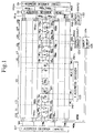
- Fig. 1 is a schematic block diagram showing the structure of a serial access memory according to the first embodiment of the present invention.
- the serial access memory has a memory cell array 101.
- An X address decoder 103 is electrically connected to the memory cell array 101.
- the X address decoder 103 is electrically connected to the plurality of word lines WL i and has a function of selecting a desired column from the memory cell array 101 in response to one of X addresses supplied from the outside.
- An input circuit 105 serves as a circuit for inputting write data input from an input terminal D in to the memory cell array 101 through a pair of write data buses WDB and WDB ⁇ .
- a Y address decoder (for writing) 107 has a function for decoding one of Y addresses supplied from the outside and selecting a desired row from the memory cell array 101 based on an address signal YW i .
- Data on the write data bus pair WDB and WDB ⁇ are input to a desired memory cell arranged in the selected row.
- a transfer circuit 109 is comprised of a plurality of transistor pairs 109 k and 109 k ⁇ . These transistors are of N channel MOS transistors (NMOSs). The transistor pairs 109k and 109k ⁇ are respectively electrically connected between the write data bus pair WDB and WDB ⁇ and flip-flops WF k of a write register 111. A desired transistor pair 109 k and 109 k ⁇ is selected based on an output YW k produced from the Y address decoder 107. The transfer circuit 109 has a function for transferring the write data on the write data bus pair WDB and WDB ⁇ to the write register 111.
- NMOSs N channel MOS transistors
- Each flip-flop WF k is comprised of two inverters WI nk and WI nk ⁇ reversely parallel-connected to each other.
- the write register 111 has a function for storing write data therein.
- a transfer circuit 113 is electrically connected between the memory cell array 101 and the write register 111 and is comprised of a plurality of transistor pairs 113 k and 113 k ⁇ . These transistors are of N channel MOS transistors (NMOSs). The transistor pairs 113 k and 113 k ⁇ are respectively electrically connected between the flip-flops WF k and the bit line pairs BL k and BL k ⁇ .
- the transfer circuit 113 has a function for writing the write data stored in the write register 111 therein and transferring the write data to the memory cell array 101 in response to a control signal PWT.
- a transfer circuit 115 for transferring read data to a first read register 117 is electrically connected to the memory cell array 101.
- the transfer circuit 115 is made up of a plurality of transistor pairs 115 k and 115 k ⁇ . These transistors correspond to N channel MOS transistors (NMOSs).
- the transistor pairs 115 k and 115 k ⁇ are respectively electrically connected between the bit line pairs BL k and BL k ⁇ and flip-flops RF k of the first read register 117. Further, the transistor pairs 115 k and 115 k ⁇ transfer data read from the memory cell array 101 to their corresponding flip-flops RF k in response to a control signal PRT1.
- Each of the flip-flops RF k is comprised of two inverters RI nk and RI nk ⁇ electrically reversely parallel-connected to one another.
- the first read register 117 has a function for storing therein read data corresponding to each column, which have been transferred from the transfer circuit 115.
- a transfer circuit 119 is electrically connected between a pair of first read data buses RD1 and RD1 ⁇ and the first read register 117 and comprises a plurality of transistor pairs 119 k and 119 k ⁇ . These transistors are of N channel MOS transistors (NMOSs). The transistor pairs 119 k and 119 k ⁇ are respectively electrically connected between the flip-flops RF k and the first read data bus pair RD1 and RD1 ⁇ . The transfer circuit 119 transfers each read data stored in the first read register 117 to the first read data bus pair RD1 and RD1 ⁇ in response to an address signal YR 1k supplied from a first Y address decoder (Read) 121.
- NMOSs N channel MOS transistors
- a first output circuit 123 is electrically connected to the first read data bus pair RD1 and RD1 ⁇ .
- the first output circuit 123 outputs each read data transferred from the first read register 117 to a first output terminal DOUT1.
- the data stored in the memory cells Q 1, a through Q m,a respectively connected to the word line WL a are read into the bit line pairs BL1 and BL1 ⁇ through BL m and BL m ⁇ to which their corresponding memory cells are electrically connected. Thereafter, the data read into the bit line pairs are amplified by sense amplifiers SA1 through SA m respectively.
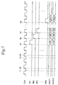
- first serial access memory of a type wherein a memory cell at an address common to the same two serial access memories provided adjacent to each other and electrically connected to an input circuit in which a write data bus common to the serial access memories is used, is selected and the same write data is written into the memory cell and data stored in memory cells at different addresses are respectively read from separately-provided output circuits in accordance with separate read operations.
- An address signal YR1 supplied from the Y address decoder (Read) 601 is brought to an "H" so that a transistor pair 1191 and 1191 ⁇ of the transfer circuit 119 and a transistor pair 1291 and 1291 ⁇ of the transfer circuit 129 are turned ON.
- read data stored in a flip-flop RF1 of a first read register 117 is transferred to an output circuit 123 through a first read data bus pair RD1 and RD1 ⁇ .
- read data stored in a flip-flop RF'1 of a second read register 127 is transferred to an output circuit 133 through a second read data bus pair RD2 and RD2 ⁇ .
- data D1 is output to the first output terminal DOUT1 from the output circuit 123 and data D1' is output to the second output terminal DOUT2 from the output circuit 133.
- the data read from the memory cell array are successively output from the two output terminals.
- serial access memory according to the second embodiment brings about the advantageous effect obtained by the serial access memory according to the first embodiment and shares the use of the read Y address decoder. It is therefore possible to realize a serial access memory which is reduced in its occupied area.
- fields to which the serial access memory according to the second embodiment is applied there are considered those such as low-grade TV and VTR, etc. which do not necessarily require the correction of a time base and are accessible under the same Y address.
- the first delay circuit 800 is activated in synchronism with a clock signal CLK.
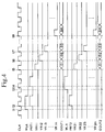
- a read operation of the serial access memory according to the present embodiment will now be described with reference to a timing chart shown in Fig. 10.
- the operation of the serial access memory according to the present embodiment can be easily understood by reference to the description of the operations of the serial access memories according to the first and second embodiments, which are shown by the timing charts of Figs. 4 and 7.
- the description of operations executed during periods t1 through t4 will be omitted by reference to the description of Figs. 4 and 7 and operations subsequent to a period t5 will be described in the present embodiment.
- An address signal YR1 supplied from a Y address decoder (Read) 601 is brought to an "H" so that a transistor pair 1191 and 1191 ⁇ of a transfer circuit 119 and a transistor pair 1291 and 1291 ⁇ of a transfer circuit 129 are turned ON.
- read data stored in a flip-flop RF1 of a first read register 117 is transferred to the first delay circuit 800 through a first read data bus pair RD1 and RD1 ⁇ . Thereafter, the read data is stored in a flip-flop FF1.
- read data stored in a flip-flop RF'1 of a second read register 127 is transferred to an output circuit 133 through a second read data bus pair RD2 and RD2 ⁇ . Thereafter, data D1' is output to the second output terminal DOUT2 from the output circuit 133.
- an address signal YR2 supplied from the Y address decoder (Read) 601 is brought to an "H" so that a transistor pair 1192 and 1192 ⁇ of the transfer circuit 119 is turned ON and a transistor pair 1292 and 1292 ⁇ of the transfer circuit 129 is turned ON.
- read data stored in a flip-flop RF2 of the first read register 117 is transferred to the first delay circuit 800 through the first read data bus pair RD1 and RD1 ⁇ .
- data stored in a flip-flop FF1 is input to a flip-flop FF2 in synchronism with the clock signal CLK and the data read from the flip-flop RF2 is input to the flip-flop FF1.
- read data stored in a flip-flop RF'2 of the second read register 127 is transferred to the output circuit 133 through the second read data bus pair RD2 and RD2 ⁇ . Thereafter, data D2' is output to the second output terminal DOUT2 from the output circuit 133.
- an address signal YR3 supplied from the Y address decoder (Read) 601 is brought to an "H" so that a transistor pair 1193 and 1193 ⁇ of the transfer circuit 119 is turned ON and a transistor pair 1293 and 1293 ⁇ of the transfer circuit 129 is turned ON.
- read data stored in a flip-flop RF3 of the first read register 117 is transferred to the first delay circuit 800 through the first read data bus pair RD1 and RD1 ⁇ .
- the data stored in the flip-flop FF1 is input to the flip-flop FF2 in synchronism with the clock signal CLK and the data stored in the flip-flop FF2 is input to a flip-flop FF3 in synchronism with the clock signal CLK.
- the data read from the flip-flop FF3 is input to the flip-flop FF1. Further, read data stored in a flip-flop RF'3 of the second read register 127 is transferred to the output circuit 133 through the second read data bus pair RD2 and RD2 ⁇ . Thereafter, data D3' is output to the second output terminal DOUT2 from the output circuit 133.
- an address signal YR4 supplied from the Y address decoder (Read) 601 is brought to an "H" so that a transistor pair 1194 and 1194 ⁇ of the transfer circuit 119 is turned ON and a transistor pair 1294 and 1294 ⁇ of the transfer circuit 129 is turned ON.
- read data stored in a flip-flop RF4 of the first read register 117 is transferred to the first delay circuit 800 through the first read data bus pair RD1 and RD1 ⁇ .
- the data stored in the flip-flop FF1 is input to the flip-flop FF2 in synchronism with the clock signal CLK and the data stored in the flip-flop FF2 is input to the flip-flop FF3 in synchronism with the clock signal CLK.
- the data read from the memory cell array are successively output from the two output terminals.
- the present embodiment can bring about an advantageous effect capable of delaying data output from one of the output terminals. It is therefore possible to increase variations in data output and make a wide range of user's choice.
- FIG. 11 is a block diagram showing the structure of a serial access memory according to the fourth embodiment of the present invention.
- the aforementioned elements are suitably blocked and typically shown to provide an easy understanding of illustration of the present embodiment.
- the same elements of structure as those described above are identified by like reference numerals and their description will therefore be omitted.
- the serial access memory according to the fourth embodiment has a delay bypass circuit 1100 electrically connected to the first delay circuit 800 employed in the serial access memory according to the third embodiment.
- the delay bypass circuit 1100 comprises transistors 1101, 1102 and 1103 and an inverter 1104. These transistors are of N-type MOS transistors.
- the transistor 1101 is electrically connected between a first read data bus pair RD1 and RD1 ⁇ and a first output circuit 123 so as to be arranged in shunt with a delay circuit 800.
- the transistor 1102 is electrically connected between a flip-flop FF1 and the first read data bus pair RD1 and RD1 ⁇ .
- the transistor 1103 is electrically connected between a flip-flop FFx and the first output circuit 123.
- a control electrode of the transistor 1101 is supplied with a delay bypass signal PBP.
- both control electrodes of the transistors 1102 and 1103 are supplied with the delay bypass signal PBP through the inverter 1104.
- the delay bypass circuit 1100 has a function for controlling a delay in data transfer in response to the delay bypass signal PBP.
- the transistor 1101 When the delay bypass signal PBP is brought to an "H" in the serial access memory according to the fourth embodiment, the transistor 1101 is turned ON and the transistors 1102 and 1103 are turned OFF. In this case, data on the read bus pair bypasses the delay circuit 800 so as to be transferred to the first output circuit 123. Namely, a delay effect is not brought about due to this bypass process.
- the delay bypass signal PBP is of a LOW LEVEL (hereinafter simply called "L")
- the transistor 1101 is turned OFF and the transistors 1102 and 1103 are turned ON.
- L LOW LEVEL
- the function of the serial access memory according to the second or third embodiment can be selected based on the delay bypass signal PBP supplied from the outside in addition to the achievement of the advantageous effects of the aforementioned embodiments.
- Fig. 13 is a block diagram showing the structure of a serial access memory according to the fifth embodiment of the present invention.
- the aforementioned elements are suitably blocked and typically shown to provide an easy understanding of illustration of the present embodiment.
- the same elements of structure as those described above are identified by like reference numerals and their description will therefore be omitted.
- the serial access memory according to the fifth embodiment is constructed such that a delay circuit 800' and a delay bypass circuit 1100' similar to those described in the third and fourth embodiments are added to the second read data bus pair RD2 and RD2 ⁇ of the serial access memory according to the fourth embodiment.
- the delay circuit 800' and the delay bypass circuit 1100' are identical in structure to the delay circuit 800 and the delay bypass circuit 1100 respectively. These circuits are controlled based on a delay bypass signal PBP'.
- serial access memory according to the present embodiment can be easily understood by reference to the third and fourth embodiments.
- the serial access memory according to the present embodiment can arbitrarily delay read data output from first and second output terminals based on a signal supplied from the outside as well as bring about the advantageous effects obtained by the aforementioned embodiments.
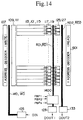
- Fig. 14 is a block diagram showing the structure of a serial access memory according to the sixth embodiment of the present invention.
- the aforementioned elements are suitably blocked and typically shown to provide an easy understanding of illustration of the present embodiment.
- the same elements of structure as those described above are identified by like reference numerals and their description will therefore be omitted.
- a delay selection circuit 1400 is electrically connected between a first read data bus pair RD1 and RD1 ⁇ and a first output circuit 123.
- the delay selection circuit 1400 comprises a plurality of transistors as shown in Fig. 15. These transistors are respectively provided between the first read data bus pair RD1 and RD1 ⁇ and the first output circuit 123 and between flip-flops FF1 through FF x and the first output circuit 123. Further, these transistors are respectively supplied with delay select signals PBP1 through PBPx. Each of the transistors is ON- or OFF-controlled according to a logic level of each delay select signal. These transistors are of N channel MOS transistors.
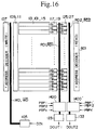
- FIG. 16 is a block diagram showing the structure of a serial access memory according to the seventh embodiment of the present invention.
- the aforementioned elements are suitably blocked and typically shown to provide an easy understanding of illustration of the present embodiment.
- the same elements of structure as those described above are identified by like reference numerals and their description will therefore be omitted.
- the present embodiment has the structure of the sixth embodiment and is constructed such that a delay selection circuit 1400' identical in structure to the delay selection circuit 1400 employed in the sixth embodiment is electrically connected between a second read data bus pair RD2 and RD2 ⁇ and a second output circuit 133.
- a detailed configuration of the delay selection circuit 1400' can be easily understood by reference to Fig. 15.
- These transistors are respectively provided between the second read data bus pair RD2 and RD2 ⁇ and the second output circuit 133 and between flip-flops FF1' through FF x ' and the second output circuit 133. Further, these transistors are respectively supplied with delay select signals PBP1' through PBPx'. Each of the transistors is ON- or OFF-controlled according to a logic level of each delay select signal.
- These transistors are of N channel MOS transistors.
- the serial access memory according to the present embodiment can select desired delay bits based on each of the delay select signals PBP1 through PBPx and each of the delay select signals PBP1' through PBPx' as well as bring about the advantageous effects obtained by the aforementioned embodiments. Therefore, a delay in data output from each of first and second output terminals can be suitably set.
- Fig. 17 is a block diagram showing the structure of a serial access memory according to the eighth embodiment of the present invention.
- the aforementioned elements are suitably blocked and typically shown to provide an easy understanding of illustration of the present embodiment.
- the same elements of structure as those described above are identified by like reference numerals and their description will therefore be omitted.
- a delay control address decoder 1700 for outputting delay select signals PBP1 through PBPx therefrom is electrically connected to the delay selection circuit 1400 employed in the serial access memory according to the sixth embodiment.
- the delay control address decoder 1700 has a function for decoding addresses AA1 through AAx supplied from the outside to control delay bits and outputting the delay select signals PBP1 through PBPx based on the result of decoding.
- the delay select signals are produced based on the external addresses in addition to the advantageous effects obtained by the aforementioned embodiments, the number of delay bits can be suitably set based on the reduced number of external signals.
- FIG. 18 is a block diagram showing the structure of a serial access memory according to the ninth embodiment of the present invention.
- the aforementioned elements are suitably blocked and typically shown to provide an easy understanding of illustration of the present embodiment.
- the same elements of structure as those described above are identified by like reference numerals and their description will therefore be omitted.
- a delay control address decoder 1700 for outputting the delay select signals PBP1 through PBPx described in the eighth embodiment and a delay control address decoder 1700' having a function equivalent to that of the delay control address decoder 1700 are respectively electrically connected to the delay selection circuit 1400 and 1400' of the serial access memory according to the seventh embodiment.
- the delay control address decoder 1700' has a function for decoding addresses AA1' through AAx' supplied from the outside to control delay bits and outputting delay select signals PBP1' through PBPx' based on the result of decoding.
- the delay select signals are produced based on the external addresses in addition to the advantageous effects obtained by the aforementioned embodiments, the number of delay bits can be suitabiy set based on the reduced number of external signals.
- Fig. 19 is a partial timing chart for describing the operation of a serial access memory according to the tenth embodiment of the present invention.
- the same elements of structure as the aforementioned elements are identified by like reference numerals to provide an easy understanding of illustration of the present embodiment and their description will therefore be omitted.
- the basic operation of the present embodiment can be easily understood by reference to the operation of the serial access memory according to the first embodiment shown in Fig. 4 and its description, and the description of the basic operation will therefore be omitted.
- Timing for providing a first read control signal PRT1 and a second read control signal PRT2, which is employed in the present embodiment, is different from that employed in the first embodiment.
- a first read control signal PRT1 is brought to an "H" during a period t2 and read data is transferred to a first read register 117 from a memory cell array 101 and stored in the first register 117.
- a second read control signal PRT2 is thereafter brought to an "H” and the read data stored in the first read register 117 is transferred to a second read register 127.
- the serial access memory can be realized which is capable of improving the efficiency of data transfer and providing a satisfactory margin of operation.
- a serial access memory according to the present embodiment is basically identical in structure to the serial access memory according to the first embodiment.
- the inverters RI nk and RI nk ⁇ of each of the flip-flops RF k and RF k ⁇ of the first read register 117 employed in the serial access memory according to the first embodiment differ in dimension from the inverters RI n'k and RI n'k ⁇ of each of the flip-flops RF k and RF k ⁇ of the second read register 127.
- the dimensions of a P channel MOS transistor (hereinafter called “PMOS”) and an N channel MOS transistor (hereinafter called “NMOS”) which respectively form the inverters RI nk and RI nk ⁇ are smaller than those of a PMOS and an NMOS which respectively form the inverters RI n'k and RI n'k ⁇ .
- the serial access memory can be realized which is capable of improving the efficiency of data transfer and providing a satisfactory margin of operation.
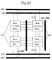
- FIGs. 20, 21 and 22 are respectively block diagrams each showing the structure of a principal part of a serial access memory according to the twelfth embodiment of the present invention.
- the aforementioned elements are suitably blocked and typically shown to provide an easy understanding of illustration of the present embodiment.
- the same elements of structure as those described above are identified by like reference numerals and their description will therefore be omitted.
- resistors R1 and R2 are respectively provided between a second read register 127 and a power source line V DD for supplying a potential to the second read register 127 and between the second read register 127 and the power source line V DD as shown in Fig. 20. Further, resistors R3 and R4 are respectively provided between a first read register 117 and power source lines V DD as shown in Fig. 21. Furthermore, resistors R1 and R2, and R3 and R4 are respectively provided between a second read register 127 and power source lines V DD and between a first read register 117 and the power source lines V DD .
- the serial access memory can be realized which is capable of improving the efficiency of data transfer and providing a satisfactory margin of operation.
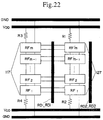
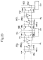
- Fig. 23 is a block diagram showing the structure of a principal part of a serial access memory according to the thirteenth embodiment of the present invention.
- the aforementioned elements are suitably blocked and typically shown to provide an easy understanding of illustration of the present embodiment.
- the same elements of structure as those described above are identified by like reference numerals and their description will therefore be omitted.
- flip-flops RF k and RF k ⁇ of a first read register 117 or flip-flops RF' k and RF' k ⁇ of a second read register 127 are respectively comprised of clocked inverters CRI nk and CRI nk ⁇ or CRI n'k and CRI n'k ⁇ . These clocked inverters are respectively controlled based on control signals ⁇ 1 and ⁇ 2.
- the serial access memory can be materialized which is capable of improving the efficiency of data transfer and providing a satisfactory margin of operation.
- Fig. 24 is a block diagram showing the structure of a principal part of a serial access memory according to the fourteenth embodiment of the present invention. In this case, the aforementioned elements are suitably blocked and typically shown to provide an easy understanding of illustration of the present embodiment.
- the serial access memory according to the present embodiment is comprised of a first serial access memory unit 2400A and a second serial access memory unit 2400B.
- a delay circuit 2403 is electrically connected between a read data bus pair RDA and RDA ⁇ of the first serial access memory unit 2400A and a write data bus pair WDB' and WDB' ⁇ of the second serial access memory unit 2400B.
- the delay circuit 2403 has a function for delaying data read from the first serial access memory unit 2400A by a predetermined period and transferring the data to the write data bus pair WDB' and WDB' ⁇ of the second serial access memory unit 2400B. The necessity of delaying the data by the delay circuit 2403 will be described later.
- the delay circuit 2403 comprises a transistor pair 2701 and 2702 electrically connected to its corresponding read data bus pair RDA and RDA ⁇ , a transistor pair 2703 and 2704 electrically connected to its corresponding write data bus pair WDB and WDB ⁇ , a flip-flop DFF electrically connected between the transistor pair 2701 and 2702 and the transistor pair 2703 and 2704 and comprised of an inverter 2705 and an inverter 2706, and an inverter 2707 for inverting a logic level of a control signal PY and supplying the inverted signal to a control electrode of the transistor pair 2703 and 2704.
- These transistors are of N channel MOS transistors.
- a read/write Y address decoder 2401 decodes outer addresses A0 and A0 ⁇ through A n and A n ⁇ and outputs address signals YRA1 through YRA n and address signals YWB1 through YWB n therefrom. These address signals YRA k and YWB k are of signals whose logic levels are equal to one another. Thus, a desired transistor pair of transistor pairs of a transfer circuit 119A is turned ON and at the same time a transistor pair corresponding to the desired transistor pair, which is selected from transistor pairs of a transfer circuit 108B, is turned ON.
- the read/write Y address decoder 2401 comprises a plurality of P channel MOS transistors (hereinafter called “PMOSs”) PT1 through PT m supplied with a precharge signal PR, a plurality of inverters I n1 through I nm , and a plurality of N channel MOS transistors (hereinafter called “NMOSs”) respectively electrically connected to terminals supplied with the outer addresses A0 and A0 ⁇ through A n and A n ⁇ .
- PMOSs P channel MOS transistors
- I n1 through I nm supplied with a precharge signal PR
- NMOSs N channel MOS transistors
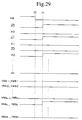
- the operation of the read/write Y address decoder 2401 is represented as an example by a timing chart shown in Fig. 29.
- the timing chart shown in Fig. 29 describes the timing for bringing each of the address signals YRA k and YWB k to the "H".
- the precharge signal PR changes from an "H” to an "L".
- the outer addresses are thereafter input during a period t2
- only the address signals YRA k and YWB k are brought to an "H” level. This is because a signal having an "H” is output from only the inverter I nk arranged in a column related to a combination of the NMOSs.
- the transistor pair 119A k and 119A k ⁇ of the transfer circuit 119A and the transistor pair 108B k and 108B k ⁇ of the transfer circuit 108B are turned ON.
- a read operation of the serial access memory according to the present embodiment will now be described with reference to Fig. 32.
- the read operation is performed on a partition base for each period to provide an easy understanding of illustration.
- nodes in a flip-flop RF1 of a read register 117A are defined as a and b as shown in Fig. 30 and nodes in a flip-flop WF2 of a write register 111B are defined as c and d as shown in Fig. 31.
- a clock signal used for the read operation is generated from the clock signal generating circuit shown in Fig. 5.
- An example in which data is transferred from the first serial access memory unit 2400A to the second serial access memory unit 2400B, will now be described on the central base. Other operations can be easily understood by referring to the operations of the aforementioned embodiments.
- a desired word line WL a (1 ⁇ a ⁇ n) is selected by an X address decoder 103A. In this case, the potential of the selected word line WL a is brought to an "H".
- the word line WL a is electrically connected to a memory cell group having data stored therein to be read from a first output terminal DOUT1A.
- bit line pairs BL1 and BL1 ⁇ through BL m and BL m ⁇ are read into bit line pairs BL1 and BL1 ⁇ through BL m and BL m ⁇ to which their corresponding memory cells are electrically connected. Thereafter, the data read into the bit line pairs are amplified by sense amplifiers SA1 through SA m respectively.
- a logic level of a first read control signal PRTA is brought to an "H". Accordingly, transistor pairs 115A1 and 115A1 ⁇ through 115A m and 115A m ⁇ of a transfer circuit 115A are turned ON.
- the data on the bit line pairs BL1 and BL1 ⁇ through BL m and BL m ⁇ which have been amplified by the sense amplifiers SA1 through SA m during the period t1, are transferred to the first read register 117A at a time.
- a clock signal CLK rises and a timing signal ⁇ P rises in synchronism with the clock signal CLK. Since the address signals YRA1 and YWB1 are output from the read/write Y address decoder 2401 at this time, a transistor pair 119A1 and 119A1 ⁇ of the transfer circuit 119A and a transistor pair 108B1 and 108B1 ⁇ of the transfer circuit 108B are turned ON. Thus, data stored in a flip-flop FF1 of the first read register 117A is transferred to the read data bus pair RDA and RDA ⁇ . Further, the data is transferred to the delay circuit 2403 so as to be stored in therein.
- the transistor pair 2703 and 2704 of the delay circuit 2403 is turned ON so that the data stored in the delay circuit 2403 is transferred to the write data bus pair WDB and WDB ⁇ .
- the transistor pair 2701 and 2702 of the delay circuit 2403 is turned ON so that the data on the read data bus pair RDA and RDA ⁇ is stored in the flip-flop DFF of the delay circuit 2403. Since a transistor pair 108B2 and 108B2 ⁇ of the transfer circuit 108B is turned ON, the data transferred onto the write data bus pair WDB and WDB ⁇ is stored in the flip-flop WF2 of the write register 111 B.
- the delay circuit is provided between the first serial access memory unit and the second serial access memory unit and the data output from the first serial access memory unit is delayed for the predetermined period. It is therefore possible to prevent a data displacement or shift corresponding to one bit from occurring when the data is written.
- the delay circuit for delaying and adjusting the shift corresponding to the one bit is provided in the serial access memory according to the- present embodiment of the present invention, a plurality of serial access memories (two serial access memories in the aforementioned embodiment) can be easily formed into one chip by using the conventional circuit design technology.
- Fig. 33 is a block diagram showing the structure of a principal part of a serial access memory according to the fifteenth embodiment of the present invention.
- the aforementioned elements are suitably blocked and typically shown to provide an easy understanding of illustration of the present embodiment.
- the same elements of structure as the aforementioned elements are identified by like reference numerals and their description will therefore be omitted.
- an initializing circuit 3300 is electrically connected to the read data bus pair RDA and RDA ⁇ employed in the serial access memory according to the fourteenth embodiment.
- the initializing circuit 3300 is comprised of transistors 3301, 3302 and 3303 and has a function for supplying an initializing predetermined potential to the read data bus pair RDA and RDA ⁇ in response to an initialization signal EQ. These transistors are of NMOSs.
- the transistor 3301 is electrically connected between the read data bus RDA ⁇ and a power source having a predetermined potential.
- the transistor 3302 is electrically connected between the read data bus RDA and the power source.
- the transistor 3303 is electrically connected between the read data bus RDA and the read data bus RDA ⁇ .
- Each of control electrodes of these transistors is supplied with the initialization signal EQ.
- the serial access memory according to the present embodiment is basically identical in operation to the serial access memory according to the fourteenth embodiment.
- the present serial access memory is different from the serial access memory according to the fourteenth embodiment in that each of the read data buses RDA and RDA ⁇ is initially set to a predetermined potential by the initializing circuit 3300 during a period in which the initialization EQ is brought to an "H".
- serial access memory The operation of the serial access memory according to the present embodiment will be described below with reference to a timing chart shown in Fig. 34.
- the description of the operation is performed on a partition base for each period in a manner similar to the above-described embodiments.
- a desired word line WL a (1 ⁇ a ⁇ n) is selected by an X address decoder 103A. In this case, the potential of the selected word line WL a is brought to an "H".
- the word line WL a is electrically connected to a memory cell group having data stored therein to be read from a first output terminal DOUT1A.
- bit line pairs BL1 and BL1 ⁇ through BL m and BL m ⁇ are read into bit line pairs BL1 and BL1 ⁇ through BL m and BL m ⁇ to which their corresponding memory cells are electrically connected. Thereafter, the data read into the bit line pairs are amplified by sense amplifiers SA1 through SA m respectively.
- a logic level of a first read control signat PRTA is brought to an "H". Accordingly, transistor pairs 115A1 and 115A1 ⁇ through 115A m and 115A m ⁇ of a transfer circuit 115A are turned ON.
- the data on the bit line pairs BL1 and BL1 ⁇ through BL m and BL m ⁇ which have been amplified by the sense amplifiers SA1 through SA m during the period t1, are transferred to a first read register 117A at a time.
- a clock signal CLK is raised and a timing signal ⁇ P rises in synchronism with the clock signal CLK. Since address signals YRA1 and YWB1 are output from a read/write Y address decoder 2401 at this time, a transistor pair 119A1 and 119A1 ⁇ of a transfer circuit 119A and a transistor pair 108B1 and 108B1 ⁇ of a transfer circuit 108B are turned ON.
- the initialization signal EQ changes from an "H” to an "L"
- data can be transferred to the read data bus pair RDA and RDA ⁇ .
- Each of the read data buses RDA and RDA ⁇ has been initially set to a power source potential before the period t3.
- data stored in a flip-flop FF1 of the first read register 117A is transferred to the read data bus pair RDA and RDA ⁇ . Further, the data is transferred to a delay circuit 2403 so as to be stored in therein.
- the data transferred to the write data bus pair WDB and WDB ⁇ during the period t4 is stored in a flop-flop WF2 of a write register 111B.
- serial access memory according to the present embodiment has the initializing circuit for the read data bus pair as well as having the advantageous effect obtained by the serial access memory according to the fourteenth embodiment, a quicker access can be carried out.
- Fig. 35 is a block diagram showing the structure of a principal part of a serial access memory according to the- sixteenth embodiment of the present invention.
- the aforementioned elements are suitably blocked and typically shown to provide an easy understanding of illustration of the present embodiment.
- the same elements of structure as the aforementioned elements are identified by like reference numerals and their description will therefore be omitted.
- a transfer circuit 108B is electrically directly connected to a memory cell array 101B without providing the write register 111B and the transfer circuit 113B of the serial access memory according to the fourteenth embodiment.
- nodes c and d are defined as nodes corresponding to the nodes c and d employed in the fourteenth embodiment.
- serial access memory according to the present embodiment, data on a write data bus pair RDA and RDA ⁇ is directly transferred to the memory cell array 101B.
- serial access memory according to the present embodiment is used in an application of such a type that the advantageous effect obtained by the fourteenth embodiment is employed and no competition is produced between the reading of data from a second serial access memory and the writing of the data into the second serial access memory, a two port memory can be realized without the write register. It is therefore possible to greatly reduce the size of a chip.
- an initializing circuit 3300 is electrically connected to the read data bus pair RDA and RDA ⁇ of the serial access memory according to the fifteenth embodiment.
- serial access memory according to the present embodiment can be understood by reference to the operations of the fourteenth through sixteenth embodiments.
- the serial access memory according to the present embodiment can provide a quicker access.
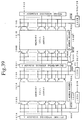
- Fig. 37 is a block diagram showing the structure of a principal part of a serial access memory according to the eighteenth embodiment of the present invention.
- the aforementioned elements are suitably blocked and typically shown to provide an easy understanding of illustration of the present embodiment.
- the same elements of structure as the aforementioned elements are identified by like reference numerals and their description will therefore be omitted.
- nodes a and b are defined as nodes corresponding to the nodes a and b employed in the fourteenth embodiment.
- serial access memory according to the present embodiment can be understood by reference to the description of the operations of the fourteenth, fifteenth and twentieth embodiments.
- serial access memory according to the present embodiment can provide a quicker access because the advantageous effect of the twentieth embodiment is obtained and the initializing circuit is provided in the present serial access memory.
- Fig. 41 is a block diagram showing the structure of a principal part of a serial access memory according to the twenty-second embodiment of the present invention.
- the aforementioned elements are suitably blocked and typically shown to provide an easy understanding of illustration of the present embodiment.
- the same elements of structure as the aforementioned elements are identified by like reference numerals and their description will therefore be omitted.
- a memory circuit 4100 is electrically connected to the write data bus pair WDB' and WDB' ⁇ of the second serial access memory unit employed in the fourteenth embodiment.
- a memory circuit 4100 is electrically connected to the write data bus pair WDB' and WDB' ⁇ of the second serial access memory unit employed in the fifteenth embodiment.
- the memory circuit 4100 since the memory circuit 4100 is electrically connected to the write data bus pair WDB' and WDB' ⁇ of the second serial access memory unit, the operation of the serial access memory is reliably ensured as well as the achievement of the advantageous effects of the fourteenth and sixteenth embodiments when the operation of the serial access memory according to the present embodiment needs to pause.
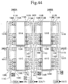
- Fig. 44 is a block diagram showing the structure of a principal part of a serial access memory according to the twenty-fourth embodiment of the present invention. In this case, the aforementioned elements are suitably blocked and typically shown to provide an easy understanding of illustration of the present embodiment.
- the serial access memory according to the present embodiment comprises a first serial access memory unit 2400A, a second serial access memory unit 2400B, a third serial access memory unit 2400C and a fourth serial access memory unit 2400D.
- a write data bus pair WDB and WDB ⁇ and a read data bus pair RDA and RDA ⁇ of the third serial access memory unit 2400C are respectively electrically connected to a write data bus pair WDB and WDB ⁇ and a read data bus pair RDA and RDA ⁇ of the first serial access memory unit 2400A.
- a write data bus pair WDB' and WDB' ⁇ and a read data bus pair RDB and RDB ⁇ of the fourth serial access memory unit 2400D are respectively electrically connected to a write data bus pair WDB' and WDB' ⁇ and a read data bus pair RDB and RDB ⁇ of the second serial access memory unit 2400B.
- Figs. 45 and 46 are respectively typical circuit block diagrams for describing the characteristic operations of the serial access memory according to the present embodiment.
- serial access memory according to the present embodiment can be operated in the above-described manner, the data writing and reading processes can be performed without interruption. It is also possible to provide a serial access memory which can bring about the advantageous effect obtained by the fourteenth embodiment and can be applied to wider uses.
- the twenty-sixth embodiment shows a case where the serial access memory according to the sixteenth embodiment is provided in the form of two banks as shown in Fig. 48 as in the case of the serial access memory according to the twenty-fourth embodiment.
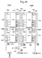
- the twenty-seventh embodiment illustrates a case where the serial access memory according to the seventeenth embodiment is provided in the form of two banks as shown in Fig. 49 as in the case of the serial access memory according to the twenty-fourth embodiment.
- the twenty-eighth embodiment depicts a case where the serial access memory according to the eighteenth embodiment is provided in the form of two banks as shown in Fig. 50 as in the case of the serial access memory according to the twenty-fourth embodiment.
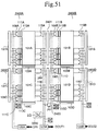
- the twenty-ninth embodiment shows a case where the serial access memory according to the nineteenth embodiment is provided in the form of two banks as shown in Fig. 51 as in the case of the serial access memory according to the twenty-fourth embodiment.
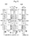
- the thirtieth embodiment illustrates a case where the serial access memory according to the twenty-second embodiment is provided in the form of two banks as shown in Fig. 52 as in the case of the serial access memory according to the twenty-fourth embodiment.
- serial access memories according to the twenty-fifth through thirty-first embodiments can be operated as described in the twenty-fourth embodiment, the data writing and reading processes can be performed without interruption. It is thus possible to provide serial access memories each of which can perform data writing and reading processes and can be applied to wider uses as well as the achievement of the advantageous effect of the fourteenth embodiment.
- Fig. 54 is a block diagram showing the structure of a principal part of a serial access memory according to the thirty-second embodiment of the present invention.
- the aforementioned elements are suitably blocked and typically shown to provide an easy understanding of illustration of the present embodiment.
- the same elements of structure as the aforementioned elements are identified by like reference numerals and their description will therefore be omitted.
- An address counter circuit 5400 for supplying a common X address to each of the X address decoders 103A and 103B employed in the above-described various embodiments is provided in the serial access memory according to the present embodiment.
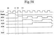
- the address counter circuit 5400 has a function for supplying X addresses A 0X , A 1X , ... A nX to the X address decoders 103A and 103B in common in response to a clock signal CLK and a reset signal Reset.
- the address counter circuit 5400 is comprised of a plurality of unit address counter circuits CNTR0 through CNTR n .
- the unit address counter circuit CNTR i comprises an inverter In1 having an input terminal supplied with the input B n-1 , a transfer gate TR1 controlled based on the output of the inverter In1 and the input B n-1 , a transfer gate TR2 controlled based on the output of the inverter In1 and the input B n-1 , a NOR gate having input terminals one of which is supplied with the reset signal Reset and the other of which is supplied with the X address A iX through the transfer gate TR1 and is electrically connected to the output of an inverter In2 through the transfer gate TR2, a transfer gate TR3 controlled based on the output of the inverter In1 and the input B n-1 , a transfer gate TR4 controlled based on the output of the inverter In1 and the input B n-1 , an inverter In4 having an input terminal electrically connected to the output of the NOR gate through the transfer gate
- the address counter circuit 5400 comprises the plurality of unit address counter circuits electrically series-connected to one another.
- the operation of the address counter circuit 5400 is represented by a partial timing chart shown in Fig. 58 as an illustrative example.
- serial access memory The operation of the serial access memory according to the present embodiment will now be described in brief with reference to Fig. 59.
- the first and second memory cell arrays 101A and 101B respectively select, for example, a word line WL1 of the first memory cell array 101A and a word line WL1 of the second memory cell array 101B in response to the same X address.
- the word line WL1 of the first memory cell array 101A is started up or activated so as to transfer data from the first memory cell array 110A to a first read register 117A (see (A) in the drawing). Thereafter, the data is delayed by one bit under the operation of a delay circuit and the delayed data is written into a second write register 111B (see (B) in the drawing). After that, a word line WL0 of the second memory cell array 101B is started up so that the contents stored in the second write register 111B are transferred to a memory cell electrically connected to the word line WL0 at a time (see (C) in the drawing).
- the data stored in the memory cell connected to the word line of the first memory cell array 101A, which has been selected based on the common X address, is transferred to the first read register 117A and is output from a first output terminal DOUT1 in response to a clock signal CLK. Further, the data is written into the second write register 111B after it has been delayed by a predetermined time interval. After completion of the writing of the data into the second write register 111B, the data is then written into the memory cell connected to the word line of the second memory cell array 101B, which has been selected based on the common X address.
- serial access memories of other inventions of the present application is constructed in the above-described manner, a plurality of conventionally-used serial access memories can be simply formed into one chip.
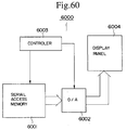
- serial access memories of the present invention can be applied to a display unit or device 6000 as shown in Fig. 60.
- serial access memories of the present invention can be applied to various fields in addition to the above application.
Landscapes
- Dram (AREA)
Applications Claiming Priority (6)
| Application Number | Priority Date | Filing Date | Title |
|---|---|---|---|
| JP28245793 | 1993-11-11 | ||
| JP282457/93 | 1993-11-11 | ||
| JP28245793 | 1993-11-11 | ||
| JP23805794A JP3732245B2 (ja) | 1993-11-11 | 1994-09-30 | シリアルアクセスメモリ |
| JP23805794 | 1994-09-30 | ||
| JP238057/94 | 1994-09-30 |
Publications (3)
| Publication Number | Publication Date |
|---|---|
| EP0653761A2 true EP0653761A2 (de) | 1995-05-17 |
| EP0653761A3 EP0653761A3 (de) | 1996-03-06 |
| EP0653761B1 EP0653761B1 (de) | 2000-07-05 |
Family
ID=26533511
Family Applications (1)
| Application Number | Title | Priority Date | Filing Date |
|---|---|---|---|
| EP94308279A Expired - Lifetime EP0653761B1 (de) | 1993-11-11 | 1994-11-10 | Serieller Zugriffspeicher |
Country Status (3)
| Country | Link |
|---|---|
| US (1) | US5812148A (de) |
| EP (1) | EP0653761B1 (de) |
| DE (1) | DE69425110T2 (de) |
Families Citing this family (5)
| Publication number | Priority date | Publication date | Assignee | Title |
|---|---|---|---|---|
| US6438043B2 (en) * | 1998-09-02 | 2002-08-20 | Micron Technology, Inc. | Adjustable I/O timing from externally applied voltage |
| JP3638857B2 (ja) | 2000-06-26 | 2005-04-13 | 沖電気工業株式会社 | シリアルアクセスメモリおよびデータライト/リード方法 |
| JP3776295B2 (ja) | 2000-06-26 | 2006-05-17 | 沖電気工業株式会社 | シリアルアクセスメモリおよびデータライト/リード方法 |
| JP3687550B2 (ja) * | 2001-02-19 | 2005-08-24 | セイコーエプソン株式会社 | 表示ドライバ、それを用いた表示ユニット及び電子機器 |
| CN1951010A (zh) * | 2003-10-10 | 2007-04-18 | 爱特梅尔股份有限公司 | 可选择延迟的脉冲发生器 |
Citations (2)
| Publication number | Priority date | Publication date | Assignee | Title |
|---|---|---|---|---|
| EP0182719A2 (de) | 1984-11-20 | 1986-05-28 | Fujitsu Limited | Halbleiterspeicher mit Schieberegistern für schnelles Lesen und Schreiben |
| JPH02187989A (ja) | 1989-01-13 | 1990-07-24 | Nec Corp | デュアルポートメモリ |
Family Cites Families (13)
| Publication number | Priority date | Publication date | Assignee | Title |
|---|---|---|---|---|
| US5142275A (en) * | 1984-12-10 | 1992-08-25 | General Electric Company | Method and means for manipulating images in a video display |
| US4683555A (en) * | 1985-01-22 | 1987-07-28 | Texas Instruments Incorporated | Serial accessed semiconductor memory with reconfigureable shift registers |
| JP2599926B2 (ja) * | 1987-08-29 | 1997-04-16 | 株式会社日立製作所 | 半導体記憶装置 |
| GB8728435D0 (en) * | 1987-12-04 | 1988-01-13 | Emi Plc Thorn | Display device |
| US5200925A (en) * | 1988-07-29 | 1993-04-06 | Mitsubishi Denki Kabushiki Kaisha | Serial access semiconductor memory device and operating method therefor |
| JPH07105914B2 (ja) * | 1990-05-23 | 1995-11-13 | 三菱電機株式会社 | 画像出力制御装置 |
| US5321658A (en) * | 1990-05-31 | 1994-06-14 | Oki Electric Industry Co., Ltd. | Semiconductor memory device being coupled by auxiliary power lines to a main power line |
| JP2530055B2 (ja) * | 1990-08-30 | 1996-09-04 | 株式会社東芝 | 半導体集積回路 |
| DE69124932D1 (de) * | 1990-10-31 | 1997-04-10 | Ibm | Video-RAM mit schnellen Rücksetzung und Kopiermöglichkeit |
| JP3316592B2 (ja) * | 1991-06-17 | 2002-08-19 | サン・マイクロシステムズ・インコーポレーテッド | 二重バッファ・出力ディスプレー・システム、および、第1のフレーム・バッファおよび第2のフレーム・バッファ相互間の切り換えを行う方法 |
| US5264837A (en) * | 1991-10-31 | 1993-11-23 | International Business Machines Corporation | Video insertion processing system |
| KR940007757Y1 (ko) * | 1991-11-14 | 1994-10-24 | 금성일렉트론 주식회사 | 반도체 패키지 |
| JP3266638B2 (ja) * | 1992-02-20 | 2002-03-18 | 沖電気工業株式会社 | マルチシリアルアクセスメモリ |
-
1994
- 1994-11-04 US US08/336,661 patent/US5812148A/en not_active Expired - Lifetime
- 1994-11-10 DE DE69425110T patent/DE69425110T2/de not_active Expired - Lifetime
- 1994-11-10 EP EP94308279A patent/EP0653761B1/de not_active Expired - Lifetime
Patent Citations (2)
| Publication number | Priority date | Publication date | Assignee | Title |
|---|---|---|---|---|
| EP0182719A2 (de) | 1984-11-20 | 1986-05-28 | Fujitsu Limited | Halbleiterspeicher mit Schieberegistern für schnelles Lesen und Schreiben |
| JPH02187989A (ja) | 1989-01-13 | 1990-07-24 | Nec Corp | デュアルポートメモリ |
Also Published As
| Publication number | Publication date |
|---|---|
| US5812148A (en) | 1998-09-22 |
| EP0653761A3 (de) | 1996-03-06 |
| EP0653761B1 (de) | 2000-07-05 |
| DE69425110D1 (de) | 2000-08-10 |
| DE69425110T2 (de) | 2001-03-22 |
Similar Documents
| Publication | Publication Date | Title |
|---|---|---|
| JP2554816B2 (ja) | 半導体記憶装置 | |
| EP0188059B1 (de) | Halbleiterspeichereinrichtung mit Lese-Änderung-Schreib-Konfiguration | |
| US5255226A (en) | Semiconductor memory device with a redundancy circuit bypassing failed memory cells | |
| KR0176739B1 (ko) | 듀얼 뱅크 메모리를 리프레시하는 회로 및 방법 | |
| US4870621A (en) | Dual port memory device with improved serial access scheme | |
| EP0503633B1 (de) | Halbleiterspeicheranordnung | |
| US4891795A (en) | Dual-port memory having pipelined serial output | |
| EP0653761A2 (de) | Serieller Zugriffspeicher | |
| US6483772B2 (en) | Semiconductor memory device capable of masking data to be written | |
| US5369618A (en) | Serial access memory | |
| EP0595251B1 (de) | Serieller Zugriffspeicher | |
| US5588133A (en) | Register block circuit for central processing unit of microcomputer | |
| JPH09161495A (ja) | 半導体メモリ装置 | |
| JP3732245B2 (ja) | シリアルアクセスメモリ | |
| EP0209893A2 (de) | Speicheranordnung | |
| US5357477A (en) | Semiconductor memory having multiple data I/O with bit aligned access function | |
| JPH07114794A (ja) | 半導体記憶装置 | |
| JP2000040356A (ja) | 感知電流の消耗を低減しうる半導体メモリ装置 | |
| EP0120485A2 (de) | Speichersystem | |
| US6445634B2 (en) | Serial access memory and data write/read method | |
| US6032222A (en) | Semiconductor memory device with simultaneously write capability | |
| JP2000076845A (ja) | 記憶装置および記憶装置の制御方法 | |
| JP3736942B2 (ja) | Rom回路 | |
| JP4264072B2 (ja) | Rom回路 | |
| JPH0831269B2 (ja) | デ−タ選択回路 |
Legal Events
| Date | Code | Title | Description |
|---|---|---|---|
| PUAI | Public reference made under article 153(3) epc to a published international application that has entered the european phase |
Free format text: ORIGINAL CODE: 0009012 |
|
| AK | Designated contracting states |
Kind code of ref document: A2 Designated state(s): DE FR GB |
|
| PUAL | Search report despatched |
Free format text: ORIGINAL CODE: 0009013 |
|
| AK | Designated contracting states |
Kind code of ref document: A3 Designated state(s): DE FR GB |
|
| 17P | Request for examination filed |
Effective date: 19960618 |
|
| 17Q | First examination report despatched |
Effective date: 19980713 |
|
| GRAG | Despatch of communication of intention to grant |
Free format text: ORIGINAL CODE: EPIDOS AGRA |
|
| GRAG | Despatch of communication of intention to grant |
Free format text: ORIGINAL CODE: EPIDOS AGRA |
|
| GRAH | Despatch of communication of intention to grant a patent |
Free format text: ORIGINAL CODE: EPIDOS IGRA |
|
| GRAH | Despatch of communication of intention to grant a patent |
Free format text: ORIGINAL CODE: EPIDOS IGRA |
|
| GRAA | (expected) grant |
Free format text: ORIGINAL CODE: 0009210 |
|
| AK | Designated contracting states |
Kind code of ref document: B1 Designated state(s): DE FR GB |
|
| REF | Corresponds to: |
Ref document number: 69425110 Country of ref document: DE Date of ref document: 20000810 |
|
| ET | Fr: translation filed | ||
| PLBE | No opposition filed within time limit |
Free format text: ORIGINAL CODE: 0009261 |
|
| STAA | Information on the status of an ep patent application or granted ep patent |
Free format text: STATUS: NO OPPOSITION FILED WITHIN TIME LIMIT |
|
| 26N | No opposition filed | ||
| GBPC | Gb: european patent ceased through non-payment of renewal fee |
Effective date: 20001110 |
|
| PG25 | Lapsed in a contracting state [announced via postgrant information from national office to epo] |
Ref country code: FR Free format text: LAPSE BECAUSE OF NON-PAYMENT OF DUE FEES Effective date: 20010731 |
|
| REG | Reference to a national code |
Ref country code: FR Ref legal event code: ST |
|
| REG | Reference to a national code |
Ref country code: GB Ref legal event code: IF02 |
|
| REG | Reference to a national code |
Ref country code: GB Ref legal event code: 728V |
|
| REG | Reference to a national code |
Ref country code: GB Ref legal event code: 728Y |
|
| REG | Reference to a national code |
Ref country code: GB Ref legal event code: 732E Free format text: REGISTERED BETWEEN 20090416 AND 20090422 |
|
| PGFP | Annual fee paid to national office [announced via postgrant information from national office to epo] |
Ref country code: DE Payment date: 20091105 Year of fee payment: 16 |
|
| PGFP | Annual fee paid to national office [announced via postgrant information from national office to epo] |
Ref country code: GB Payment date: 20091104 Year of fee payment: 16 |
|
| GBPC | Gb: european patent ceased through non-payment of renewal fee |
Effective date: 20101110 |
|
| REG | Reference to a national code |
Ref country code: DE Ref legal event code: R119 Ref document number: 69425110 Country of ref document: DE Effective date: 20110601 Ref country code: DE Ref legal event code: R119 Ref document number: 69425110 Country of ref document: DE Effective date: 20110531 |
|
| PG25 | Lapsed in a contracting state [announced via postgrant information from national office to epo] |
Ref country code: DE Free format text: LAPSE BECAUSE OF NON-PAYMENT OF DUE FEES Effective date: 20110531 |
|
| PG25 | Lapsed in a contracting state [announced via postgrant information from national office to epo] |
Ref country code: GB Free format text: LAPSE BECAUSE OF NON-PAYMENT OF DUE FEES Effective date: 20101110 |