EP0654545A1 - Dispositif semi-conducteur à couche mince et procédé de fabrication - Google Patents
Dispositif semi-conducteur à couche mince et procédé de fabrication Download PDFInfo
- Publication number
- EP0654545A1 EP0654545A1 EP94113308A EP94113308A EP0654545A1 EP 0654545 A1 EP0654545 A1 EP 0654545A1 EP 94113308 A EP94113308 A EP 94113308A EP 94113308 A EP94113308 A EP 94113308A EP 0654545 A1 EP0654545 A1 EP 0654545A1
- Authority
- EP
- European Patent Office
- Prior art keywords
- thin film
- gas
- reaction
- plasma
- semiconductor device
- Prior art date
- Legal status (The legal status is an assumption and is not a legal conclusion. Google has not performed a legal analysis and makes no representation as to the accuracy of the status listed.)
- Withdrawn
Links
Images



Classifications
-
- H—ELECTRICITY
- H10—SEMICONDUCTOR DEVICES; ELECTRIC SOLID-STATE DEVICES NOT OTHERWISE PROVIDED FOR
- H10P—GENERIC PROCESSES OR APPARATUS FOR THE MANUFACTURE OR TREATMENT OF DEVICES COVERED BY CLASS H10
- H10P14/00—Formation of materials, e.g. in the shape of layers or pillars
- H10P14/60—Formation of materials, e.g. in the shape of layers or pillars of insulating materials
- H10P14/69—Inorganic materials
- H10P14/692—Inorganic materials composed of oxides, glassy oxides or oxide-based glasses
- H10P14/6921—Inorganic materials composed of oxides, glassy oxides or oxide-based glasses containing silicon
- H10P14/6922—Inorganic materials composed of oxides, glassy oxides or oxide-based glasses containing silicon the material containing Si, O and at least one of H, N, C, F or other non-metal elements, e.g. SiOC, SiOC:H or SiONC
- H10P14/6924—Inorganic materials composed of oxides, glassy oxides or oxide-based glasses containing silicon the material containing Si, O and at least one of H, N, C, F or other non-metal elements, e.g. SiOC, SiOC:H or SiONC the material being halogen doped silicon oxides, e.g. FSG
-
- C—CHEMISTRY; METALLURGY
- C23—COATING METALLIC MATERIAL; COATING MATERIAL WITH METALLIC MATERIAL; CHEMICAL SURFACE TREATMENT; DIFFUSION TREATMENT OF METALLIC MATERIAL; COATING BY VACUUM EVAPORATION, BY SPUTTERING, BY ION IMPLANTATION OR BY CHEMICAL VAPOUR DEPOSITION, IN GENERAL; INHIBITING CORROSION OF METALLIC MATERIAL OR INCRUSTATION IN GENERAL
- C23C—COATING METALLIC MATERIAL; COATING MATERIAL WITH METALLIC MATERIAL; SURFACE TREATMENT OF METALLIC MATERIAL BY DIFFUSION INTO THE SURFACE, BY CHEMICAL CONVERSION OR SUBSTITUTION; COATING BY VACUUM EVAPORATION, BY SPUTTERING, BY ION IMPLANTATION OR BY CHEMICAL VAPOUR DEPOSITION, IN GENERAL
- C23C16/00—Chemical coating by decomposition of gaseous compounds, without leaving reaction products of surface material in the coating, i.e. chemical vapour deposition [CVD] processes
- C23C16/22—Chemical coating by decomposition of gaseous compounds, without leaving reaction products of surface material in the coating, i.e. chemical vapour deposition [CVD] processes characterised by the deposition of inorganic material, other than metallic material
- C23C16/30—Deposition of compounds, mixtures or solid solutions, e.g. borides, carbides, nitrides
- C23C16/40—Oxides
- C23C16/401—Oxides containing silicon
-
- C—CHEMISTRY; METALLURGY
- C23—COATING METALLIC MATERIAL; COATING MATERIAL WITH METALLIC MATERIAL; CHEMICAL SURFACE TREATMENT; DIFFUSION TREATMENT OF METALLIC MATERIAL; COATING BY VACUUM EVAPORATION, BY SPUTTERING, BY ION IMPLANTATION OR BY CHEMICAL VAPOUR DEPOSITION, IN GENERAL; INHIBITING CORROSION OF METALLIC MATERIAL OR INCRUSTATION IN GENERAL
- C23C—COATING METALLIC MATERIAL; COATING MATERIAL WITH METALLIC MATERIAL; SURFACE TREATMENT OF METALLIC MATERIAL BY DIFFUSION INTO THE SURFACE, BY CHEMICAL CONVERSION OR SUBSTITUTION; COATING BY VACUUM EVAPORATION, BY SPUTTERING, BY ION IMPLANTATION OR BY CHEMICAL VAPOUR DEPOSITION, IN GENERAL
- C23C16/00—Chemical coating by decomposition of gaseous compounds, without leaving reaction products of surface material in the coating, i.e. chemical vapour deposition [CVD] processes
- C23C16/22—Chemical coating by decomposition of gaseous compounds, without leaving reaction products of surface material in the coating, i.e. chemical vapour deposition [CVD] processes characterised by the deposition of inorganic material, other than metallic material
- C23C16/30—Deposition of compounds, mixtures or solid solutions, e.g. borides, carbides, nitrides
- C23C16/40—Oxides
- C23C16/401—Oxides containing silicon
- C23C16/402—Silicon dioxide
-
- C—CHEMISTRY; METALLURGY
- C23—COATING METALLIC MATERIAL; COATING MATERIAL WITH METALLIC MATERIAL; CHEMICAL SURFACE TREATMENT; DIFFUSION TREATMENT OF METALLIC MATERIAL; COATING BY VACUUM EVAPORATION, BY SPUTTERING, BY ION IMPLANTATION OR BY CHEMICAL VAPOUR DEPOSITION, IN GENERAL; INHIBITING CORROSION OF METALLIC MATERIAL OR INCRUSTATION IN GENERAL
- C23C—COATING METALLIC MATERIAL; COATING MATERIAL WITH METALLIC MATERIAL; SURFACE TREATMENT OF METALLIC MATERIAL BY DIFFUSION INTO THE SURFACE, BY CHEMICAL CONVERSION OR SUBSTITUTION; COATING BY VACUUM EVAPORATION, BY SPUTTERING, BY ION IMPLANTATION OR BY CHEMICAL VAPOUR DEPOSITION, IN GENERAL
- C23C16/00—Chemical coating by decomposition of gaseous compounds, without leaving reaction products of surface material in the coating, i.e. chemical vapour deposition [CVD] processes
- C23C16/44—Chemical coating by decomposition of gaseous compounds, without leaving reaction products of surface material in the coating, i.e. chemical vapour deposition [CVD] processes characterised by the method of coating
- C23C16/50—Chemical coating by decomposition of gaseous compounds, without leaving reaction products of surface material in the coating, i.e. chemical vapour deposition [CVD] processes characterised by the method of coating using electric discharges
- C23C16/517—Chemical coating by decomposition of gaseous compounds, without leaving reaction products of surface material in the coating, i.e. chemical vapour deposition [CVD] processes characterised by the method of coating using electric discharges using a combination of discharges covered by two or more of groups C23C16/503 - C23C16/515
-
- H—ELECTRICITY
- H10—SEMICONDUCTOR DEVICES; ELECTRIC SOLID-STATE DEVICES NOT OTHERWISE PROVIDED FOR
- H10P—GENERIC PROCESSES OR APPARATUS FOR THE MANUFACTURE OR TREATMENT OF DEVICES COVERED BY CLASS H10
- H10P14/00—Formation of materials, e.g. in the shape of layers or pillars
- H10P14/60—Formation of materials, e.g. in the shape of layers or pillars of insulating materials
- H10P14/63—Formation of materials, e.g. in the shape of layers or pillars of insulating materials characterised by the formation processes
- H10P14/6326—Deposition processes
- H10P14/6328—Deposition from the gas or vapour phase
- H10P14/6334—Deposition from the gas or vapour phase using decomposition or reaction of gaseous or vapour phase compounds, i.e. chemical vapour deposition
- H10P14/6336—Deposition from the gas or vapour phase using decomposition or reaction of gaseous or vapour phase compounds, i.e. chemical vapour deposition in the presence of a plasma [PECVD]
-
- H—ELECTRICITY
- H10—SEMICONDUCTOR DEVICES; ELECTRIC SOLID-STATE DEVICES NOT OTHERWISE PROVIDED FOR
- H10P—GENERIC PROCESSES OR APPARATUS FOR THE MANUFACTURE OR TREATMENT OF DEVICES COVERED BY CLASS H10
- H10P14/00—Formation of materials, e.g. in the shape of layers or pillars
- H10P14/60—Formation of materials, e.g. in the shape of layers or pillars of insulating materials
- H10P14/66—Formation of materials, e.g. in the shape of layers or pillars of insulating materials characterised by the type of materials
- H10P14/668—Formation of materials, e.g. in the shape of layers or pillars of insulating materials characterised by the type of materials the materials being characterised by the deposition precursor materials
- H10P14/6681—Formation of materials, e.g. in the shape of layers or pillars of insulating materials characterised by the type of materials the materials being characterised by the deposition precursor materials the precursor containing a compound comprising Si
Definitions
- This invention relates to a method for forming thin film semiconductor devices using plasma enhanced CVD to form a thin film on a sample surface such as a semiconductor substrate, etc.
- the plasma enhanced CVD method whereby a plasma is produced in a reaction vessel, and the reaction gas introduced into this reaction vessel is activated using plasma discharge energy, thereby promoting the deposition of a deposit formed by chemical vapor growth of the reaction gas on the sample surface, was widely used as a means of forming a thin film on a semiconductor substrate or other sample surface.
- a single frequency alternating current at 13.56 MHz, 400 kHz, etc. is applied between opposing electrodes erected within the reaction vessel, and said alternating current adjusted to control deposition speed and quality of the thin film formed, or the method whereby a 2.54 GHz microwave is guided to the reaction vessel through a waveguide.
- Gases used for the reaction gas included for the deposition of SiO2 and SiON on the surface of a semiconductor substrate are, for example TEOS (tetraethyl orthosilicate) gas and SiH4 gas.
- TEOS tetraethyl orthosilicate
- Figures 6 (a) - (f) show the vertical sectional shape obtained when, in a conventional plasma-enhanced CVD (referred to below as PECVD), which generates a plasma in a reaction vessel by applying a 13.56 MHz single frequency power between the above opposing electrodes, the introduction of SiH4 gas causes an insulating covering of SiO2, to be formed on the SiO2 oxide layer on the semiconductor substrate surface and Al wiring formed on that surface.
- PECVD plasma-enhanced CVD
- the SiO2 thin film has a sectional shape in which that side has ridges and roundness following the depressions and ridges of the foundation surface.
- the film thickness is greater in the region of the Al wiring upper side than in the region of the Al wiring lower side, the problem arises that voids are created in the region of the lower side of the Al wiring. This invites an extremely serious problem in high density wiring (see Figures 6 (e) and (f)) when the space between voids in Al wiring grows very small, as in the submicron [environment].
- Figures 7 (a) - (f) depict the experimental results (vertical section) of the case where, in a conventional two frequency excitation-type PECVD equipment, wherein a plasma is generated in a reaction vessel by simultaneously applying a high frequency power of 13.56 MHz and a low frequency power of 400 kHz between the aforementioned opposing electrodes, the introduction of a TEOS gas causes an SiO2 thin film to act as an insulating covering to be further formed on the semiconductor substrate surface SiO2 oxide film and on the Al wiring formed on the surface thereof (in other words, on top of the foundation).
- the purpose of this invention is to offer a semiconductor device thin film formation method which takes note of the problems inherent in this conventional PECVD method, and which is capable of handling ever higher densities.
- the invention has as its object a semiconductor device thin film forming method characterized as follows: multiple alternating current power sources of differing frequencies or a power source of a single frequency are used to generate a plasma in a reactor vessel; by activating a reaction gas introduced to this reaction vessel using plasma discharge energy, a deposit is formed by chemical growth of the reaction gas on a sample surface, and, as the above reaction gas, the invention applies a mixed gas of TEOS gas with a SiX n R 4-n , (where 1 ⁇ n ⁇ 3, Si is silicon, X is a halogen substituent, and R is an alkoxy group) silicon halide hydrocarbon gas.
- the "X" halogen substituent in the above halogen carbide hydrocarbon gas is one of the following: fluorine "F”, chlorine “Cl", or bromine “Br", and the alkoxy base "R" above is one of the following: hydrogen "H”, methoxy "OCH3", ethoxy "OC2H5", n-propoxy "OC3H7", i-propoxy "OCH(CH3)2", n-butoxy "OC4H9", i-butoxy "OCH2CH(CH3)2", s-butoxy "OC(CH3)C2H5", or t-butoxy "OC(CH3)3)".
- SiF(OC2H5)3 made up of fluorine "F” for the above halogen substituent "X” and ethoxy "OC2H5" as the above alkoxy group "R".
- the side walls of the thin film When a thin film is formed on the rough surface of the foundation material using TEOS gas and silicon halide hydrocarbon gas as the above reaction gases, the side walls of the thin film will be formed in a regularly tapered shape in conformance with that roughness; the thin film will favorably invade and be finely formed in the depressions thereof, so that even if the surface of the foundation material is rough, the surface of the thin film will be flat.
- the side walls of the thin film are not formed in a reverse tapered manner, but display superior filling characteristics, so voids do not form in the depression of the foundation material.
- the thin film formed includes halogen elements such as fluorine in the film, making it low in electrical inductance, it becomes possible to improve the electrical characteristics of transistors, etc.
- Opposing electrodes 3 and 4 are housed in insulating reaction vessel 2 used to implement reaction chamber 1, which is sealed from the atmosphere.
- One of these electrodes 4 is held at ground potential while a semiconductor substrate 5 for thin film formation is affixed to the opposite surface; the power used to generate a plasma is applied to the other electrode 3.
- the reaction gas is introduced from the upper side of electrode 3 through pipe 6 to reaction chamber 1, while the inside of reaction chamber 1 is put into a condition of negative pressure by exhausting one side of reactor vessel 2.
- a high frequency power of, for example, 13.56 MHz is applied from high frequency power supply 8 to electrode 3 through impedance matching circuit 9, while at the same time a low frequency power of, for example, 400 kHz is applied from low frequency power supply 10 to electrode 3 through impedance matching circuit 11 and high frequency cutoff filter circuit 12, which prevents the passing of the high frequency component. That is to say, by simultaneously applying two frequencies of alternating current to electrode 3, a plasma is generated in reaction chamber 1.
- reaction gas described below (a mixed gas) is introduced into reaction chamber 1, the output power ratio of high frequency power supply 8 and low frequency power supply 10 are adjusted to activate this reaction gas with plasma discharge energy, and a SiO2 film is formed on the surface of semiconductor substrate 5.
- SiX n R 4-n (where 1 ⁇ n ⁇ 3; Si is silicon, X is a halogen substituent and R is an alkoxy group);
- the "X" halogen substituent in the above halogen carbide hydrocarbon gas is one of the following: fluorine "F”, chlorine “Cl", and bromine “Br”, and the alkoxy group "R” is one of the following: hydrogen "H”, methoxy "OCH3", ethoxy "OC2H5", n-propoxy "OC3H7", i-propoxy "OCH(CH3)2", n-butoxy "OC4H9", i-butoxy "OCH2CH(CH3)2", s-butoxy "OC(CH3)C2H5)", and t-butoxy "OC(CH3)3)".
- the silicon halide hydrocarbon gas in which the alide substituent (C) is fluorine (F) and the alkoxy group (R) is ethoxy (OC2H5) is SiF(OC2H5)3.
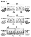
- Figures 2 (a) - (f) depict a vertical section of the case where a SiO2 thin film is formed as an insulating cover over the foundation material on top of the semiconductor substrate surface SiO2 oxide film and the Al wiring formed thereon which is to say on a rough surface by the formation manufacturing stage which makes use of a mixture (reaction gas) of TEOS gas and silicon halide hydrocarbon gas, for example a mixture of the above TEOS gas with a SiF (OC2H5)3 gas.
- a mixture (reaction gas) of TEOS gas and silicon halide hydrocarbon gas for example a mixture of the above TEOS gas with a SiF (OC2H5)3 gas.
- the section has been traced from the contours of a micrograph taken of the vertical section; the height and width are as depicted by the unit scale (0.5 ⁇ m) included in the diagram.
- the surface layer (surface) of the SiO2 thin film is somewhat rough in conformance with the roughness of the foundation material when the interstitial spacing within the Al wiring is relatively large, but because of the superior filling characteristics displayed with respect to depressions in the foundation material, that surface is flat when compared to the conventional technology (see Figures 6 and 7). Furthermore, even if the surface of that SiO2 thin film is somewhat rough owing to the roughness of the foundation material, the sloped side walls of those depressions and ridges are formed with a regular taper, so the occurrence of voids is greatly reduced.
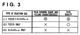
- Figure 3 shows the results of an evaluation of film shape and filling characteristics versus film quality using the same manufacturing equipment using (1) a mixture of TEOS gas and silicon halide hydrocarbon gas per the invention, (2) conventional TEOS gas only, and (3) silicon halide hydrocarbon only.
- "X" indicates that favorable results were not obtained; a single “O” indicates relatively favorable results, and a double “o” indicates superior results.
- the SiO2 thin film favorably invades and densely fills the depressions in the roughness caused by the Al wiring. Furthermore, regardless of the fine manufacturing conditions, because of the superior filling characteristics achieved, there is no occurrence of voids in the depressions on the foundation material.
- the fact that the fineness of the SiO2 thin film is favorable means that it is possible to offer a method with superior film quality controllability. Furthermore, because the thin film formed includes halogen elements such as fluorine in the film, making it low in electrical inductance, it becomes possible to improve the electrical characteristics of transistors, etc.
- the same superior thin film formation can also be achieved by applying the reaction gas of the invention using ECR plasma CVD equipment, induction coupled RF high density plasma CVD equipment, helicon wave RF high density plasma CVD equipment, etc.
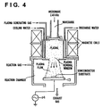
- a 2.45 GHz microwave for example, is guided through a waveguide to the plasma generation chamber in the ECR plasma CVD equipment which is outlined in Figure 4.
- the gas used for generating a plasma N2
- the various gas mixtures described above are introduced to the reaction chamber as reaction gases.
- the thin film which is to be formed on a semiconductor substrate, etc., is then formed on the attaching electrode 13 by applying a high frequency power, for example of 13.56 MHz, from high frequency power supply 14.
- a plasma is formed by a high frequency power of, for example, 2.0 MHz supplied to the induction coil in the reaction chamber of the induction coupled RF high density plasma CVD equipment whose outline is shown in Figure 5, while at the same time the reaction gas of the invention is introduced to the reaction chamber.
- the thin film which is to be formed on a semiconductor substrate, etc., is then formed on the attaching electrode 15 by the application of a high frequency power of, for example 1.8 MHz from high frequency power supply 16 through impedance matching circuit 17.
- the invention as described above provides a method whereby multiple alternating current power sources of differing frequencies or a power source of a single frequency are used to generate a plasma in a reactor vessel; by activating a reaction gas introduced to this reaction vessel using plasma discharge energy, a deposit is formed by chemical growth of the reaction gas to be deposited on a sample surface; in this method a mixture of TEOS and silicon halide hydrocarbon gases are used for the reaction gas, so even when the thin film is formed on the surface of foundation material with a rough surface, there is no occurrence of voids, since the side walls and surface walls of the thin film are flat. Because of the favorable fineness of the thin film, it is possible to offer a method with superior film quality controllability.
- the thin film formed includes halogen elements such as fluorine in the film, making it low in electrical inductance, it becomes possible to improve the electrical characteristics of transistors, etc.
- halogen elements such as fluorine in the film
Landscapes
- Chemical & Material Sciences (AREA)
- Engineering & Computer Science (AREA)
- Materials Engineering (AREA)
- General Chemical & Material Sciences (AREA)
- Chemical Kinetics & Catalysis (AREA)
- Mechanical Engineering (AREA)
- Metallurgy (AREA)
- Organic Chemistry (AREA)
- Inorganic Chemistry (AREA)
- Plasma & Fusion (AREA)
- Physics & Mathematics (AREA)
- Chemical Vapour Deposition (AREA)
- Formation Of Insulating Films (AREA)
Applications Claiming Priority (2)
| Application Number | Priority Date | Filing Date | Title |
|---|---|---|---|
| JP291926/93 | 1993-11-22 | ||
| JP5291926A JPH07193004A (ja) | 1993-11-22 | 1993-11-22 | 半導体装置の薄膜形成方法 |
Publications (1)
| Publication Number | Publication Date |
|---|---|
| EP0654545A1 true EP0654545A1 (fr) | 1995-05-24 |
Family
ID=17775256
Family Applications (1)
| Application Number | Title | Priority Date | Filing Date |
|---|---|---|---|
| EP94113308A Withdrawn EP0654545A1 (fr) | 1993-11-22 | 1994-08-25 | Dispositif semi-conducteur à couche mince et procédé de fabrication |
Country Status (3)
| Country | Link |
|---|---|
| EP (1) | EP0654545A1 (fr) |
| JP (1) | JPH07193004A (fr) |
| KR (1) | KR950015560A (fr) |
Cited By (2)
| Publication number | Priority date | Publication date | Assignee | Title |
|---|---|---|---|---|
| EP0724286A1 (fr) * | 1995-01-25 | 1996-07-31 | Applied Materials, Inc. | Méthode de formation d'un film mince d'oxyde de silicium pour un composant à semi-conducteur |
| EP0761841A1 (fr) * | 1995-08-18 | 1997-03-12 | Canon Sales Co., Inc. | Procédé de formation d'une couche |
Citations (1)
| Publication number | Priority date | Publication date | Assignee | Title |
|---|---|---|---|---|
| EP0517548A2 (fr) * | 1991-06-07 | 1992-12-09 | Nec Corporation | Méthode de dépôt chimique en phase vapeur pour fabriquer un film d'oxyde de silicium |
Family Cites Families (3)
| Publication number | Priority date | Publication date | Assignee | Title |
|---|---|---|---|---|
| JPS5930130A (ja) * | 1982-08-10 | 1984-02-17 | Kazuyuki Kinoshita | 入力装置 |
| DE69026756T2 (de) * | 1989-06-22 | 1996-11-07 | Watkins Johnson Co | Methode und Anordnung zur Ablagerung einer Siliciumdioxydschicht |
| JPH05164831A (ja) * | 1991-12-17 | 1993-06-29 | Furuno Electric Co Ltd | 航跡表示装置 |
-
1993
- 1993-11-22 JP JP5291926A patent/JPH07193004A/ja active Pending
-
1994
- 1994-08-23 KR KR1019940020729A patent/KR950015560A/ko not_active Ceased
- 1994-08-25 EP EP94113308A patent/EP0654545A1/fr not_active Withdrawn
Patent Citations (1)
| Publication number | Priority date | Publication date | Assignee | Title |
|---|---|---|---|---|
| EP0517548A2 (fr) * | 1991-06-07 | 1992-12-09 | Nec Corporation | Méthode de dépôt chimique en phase vapeur pour fabriquer un film d'oxyde de silicium |
Cited By (3)
| Publication number | Priority date | Publication date | Assignee | Title |
|---|---|---|---|---|
| EP0724286A1 (fr) * | 1995-01-25 | 1996-07-31 | Applied Materials, Inc. | Méthode de formation d'un film mince d'oxyde de silicium pour un composant à semi-conducteur |
| EP0761841A1 (fr) * | 1995-08-18 | 1997-03-12 | Canon Sales Co., Inc. | Procédé de formation d'une couche |
| US5800877A (en) * | 1995-08-18 | 1998-09-01 | Canon Sales Co., Inc. | Method for forming a fluorine containing silicon oxide film |
Also Published As
| Publication number | Publication date |
|---|---|
| KR950015560A (ko) | 1995-06-17 |
| JPH07193004A (ja) | 1995-07-28 |
Similar Documents
| Publication | Publication Date | Title |
|---|---|---|
| US6217785B1 (en) | Scavenging fluorine in a planar inductively coupled plasma reactor | |
| US5531834A (en) | Plasma film forming method and apparatus and plasma processing apparatus | |
| KR0160958B1 (ko) | 실리콘 이산화물을 증착시키는 집적회로 제조방법 | |
| JP3238082B2 (ja) | 電子デバイス製造装置 | |
| JPH02236282A (ja) | 有機珪素化合物と三弗化窒素を用いた珪素含有被膜の製法 | |
| KR19990077209A (ko) | 플라즈마 성막방법 및 플라즈마 성막장치 | |
| US5772832A (en) | Process for etching oxides in an electromagnetically coupled planar plasma apparatus | |
| US5302555A (en) | Anisotropic deposition of dielectrics | |
| US6607790B1 (en) | Method of forming a thin film for a semiconductor device | |
| JP4356747B2 (ja) | 高密度プラズマ化学蒸着を用いた間隙充填方法及び材料蒸着方法 | |
| US6090303A (en) | Process for etching oxides in an electromagnetically coupled planar plasma apparatus | |
| CN111154490A (zh) | 刻蚀气体、刻蚀方法及3d存储器件制造方法 | |
| TWI904621B (zh) | 緻密的無縫矽間隙填充製程 | |
| JP2916119B2 (ja) | 薄膜形成方法 | |
| US20240420950A1 (en) | Densified seam-free silicon-containing material gap fill processes | |
| EP0724286A1 (fr) | Méthode de formation d'un film mince d'oxyde de silicium pour un composant à semi-conducteur | |
| JP3134875B2 (ja) | プラズマ気相反応装置 | |
| JPH06208972A (ja) | プラズマ処理方法 | |
| JPS6248759B2 (fr) | ||
| US7026172B2 (en) | Reduced thickness variation in a material layer deposited in narrow and wide integrated circuit trenches | |
| EP1039501A2 (fr) | Appareil et procédé pour la fabrication d'un dispositif semi-conducteur | |
| JPH088237B2 (ja) | プラズマ処理方法 | |
| JPH07193004A (ja) | 半導体装置の薄膜形成方法 | |
| JPH0467777B2 (fr) | ||
| TW389963B (en) | Method of depositing uniform dielectric layers |
Legal Events
| Date | Code | Title | Description |
|---|---|---|---|
| PUAI | Public reference made under article 153(3) epc to a published international application that has entered the european phase |
Free format text: ORIGINAL CODE: 0009012 |
|
| AK | Designated contracting states |
Kind code of ref document: A1 Designated state(s): DE FR GB IT NL |
|
| 17P | Request for examination filed |
Effective date: 19951124 |
|
| 17Q | First examination report despatched |
Effective date: 19961127 |
|
| STAA | Information on the status of an ep patent application or granted ep patent |
Free format text: STATUS: THE APPLICATION IS DEEMED TO BE WITHDRAWN |
|
| 18D | Application deemed to be withdrawn |
Effective date: 19970408 |