EP0655726A1 - Graupegelwählende Schaltung für eine Anzeigesteuerschaltung - Google Patents
Graupegelwählende Schaltung für eine Anzeigesteuerschaltung Download PDFInfo
- Publication number
- EP0655726A1 EP0655726A1 EP94307896A EP94307896A EP0655726A1 EP 0655726 A1 EP0655726 A1 EP 0655726A1 EP 94307896 A EP94307896 A EP 94307896A EP 94307896 A EP94307896 A EP 94307896A EP 0655726 A1 EP0655726 A1 EP 0655726A1
- Authority
- EP
- European Patent Office
- Prior art keywords
- gray
- scale voltage
- oscillating
- bits
- signals
- Prior art date
- Legal status (The legal status is an assumption and is not a legal conclusion. Google has not performed a legal analysis and makes no representation as to the accuracy of the status listed.)
- Granted
Links
- 241001270131 Agaricus moelleri Species 0.000 claims abstract description 28
- 238000010586 diagram Methods 0.000 description 21
- 230000007274 generation of a signal involved in cell-cell signaling Effects 0.000 description 20
- 238000005070 sampling Methods 0.000 description 18
- 239000004973 liquid crystal related substance Substances 0.000 description 8
- 238000010276 construction Methods 0.000 description 5
- 230000000694 effects Effects 0.000 description 5
- 239000011159 matrix material Substances 0.000 description 5
- 230000003247 decreasing effect Effects 0.000 description 4
- 238000013461 design Methods 0.000 description 4
- 239000011521 glass Substances 0.000 description 3
- 238000004519 manufacturing process Methods 0.000 description 3
- 238000000034 method Methods 0.000 description 3
- 239000000758 substrate Substances 0.000 description 3
- 102100040623 60S ribosomal protein L41 Human genes 0.000 description 2
- 101100172073 Echinococcus granulosus EG13 gene Proteins 0.000 description 2
- 101000674326 Homo sapiens 60S ribosomal protein L41 Proteins 0.000 description 2
- 230000000630 rising effect Effects 0.000 description 2
- 238000005549 size reduction Methods 0.000 description 2
- 101150070189 CIN3 gene Proteins 0.000 description 1
- 101150110971 CIN7 gene Proteins 0.000 description 1
- 101100286980 Daucus carota INV2 gene Proteins 0.000 description 1
- 101100508840 Daucus carota INV3 gene Proteins 0.000 description 1
- 101150110298 INV1 gene Proteins 0.000 description 1
- 101100397044 Xenopus laevis invs-a gene Proteins 0.000 description 1
- 101100397045 Xenopus laevis invs-b gene Proteins 0.000 description 1
- 238000007796 conventional method Methods 0.000 description 1
- 238000009434 installation Methods 0.000 description 1
- 238000012986 modification Methods 0.000 description 1
- 230000004048 modification Effects 0.000 description 1
- 239000010409 thin film Substances 0.000 description 1
Images


Classifications
-
- G—PHYSICS
- G02—OPTICS
- G02F—OPTICAL DEVICES OR ARRANGEMENTS FOR THE CONTROL OF LIGHT BY MODIFICATION OF THE OPTICAL PROPERTIES OF THE MEDIA OF THE ELEMENTS INVOLVED THEREIN; NON-LINEAR OPTICS; FREQUENCY-CHANGING OF LIGHT; OPTICAL LOGIC ELEMENTS; OPTICAL ANALOGUE/DIGITAL CONVERTERS
- G02F1/00—Devices or arrangements for the control of the intensity, colour, phase, polarisation or direction of light arriving from an independent light source, e.g. switching, gating or modulating; Non-linear optics
- G02F1/01—Devices or arrangements for the control of the intensity, colour, phase, polarisation or direction of light arriving from an independent light source, e.g. switching, gating or modulating; Non-linear optics for the control of the intensity, phase, polarisation or colour
- G02F1/13—Devices or arrangements for the control of the intensity, colour, phase, polarisation or direction of light arriving from an independent light source, e.g. switching, gating or modulating; Non-linear optics for the control of the intensity, phase, polarisation or colour based on liquid crystals, e.g. single liquid crystal display cells
- G02F1/133—Constructional arrangements; Operation of liquid crystal cells; Circuit arrangements
- G02F1/136—Liquid crystal cells structurally associated with a semi-conducting layer or substrate, e.g. cells forming part of an integrated circuit
-
- G—PHYSICS
- G09—EDUCATION; CRYPTOGRAPHY; DISPLAY; ADVERTISING; SEALS
- G09G—ARRANGEMENTS OR CIRCUITS FOR CONTROL OF INDICATING DEVICES USING STATIC MEANS TO PRESENT VARIABLE INFORMATION
- G09G3/00—Control arrangements or circuits, of interest only in connection with visual indicators other than cathode-ray tubes
- G09G3/20—Control arrangements or circuits, of interest only in connection with visual indicators other than cathode-ray tubes for presentation of an assembly of a number of characters, e.g. a page, by composing the assembly by combination of individual elements arranged in a matrix no fixed position being assigned to or needed to be assigned to the individual characters or partial characters
- G09G3/34—Control arrangements or circuits, of interest only in connection with visual indicators other than cathode-ray tubes for presentation of an assembly of a number of characters, e.g. a page, by composing the assembly by combination of individual elements arranged in a matrix no fixed position being assigned to or needed to be assigned to the individual characters or partial characters by control of light from an independent source
- G09G3/36—Control arrangements or circuits, of interest only in connection with visual indicators other than cathode-ray tubes for presentation of an assembly of a number of characters, e.g. a page, by composing the assembly by combination of individual elements arranged in a matrix no fixed position being assigned to or needed to be assigned to the individual characters or partial characters by control of light from an independent source using liquid crystals
- G09G3/3611—Control of matrices with row and column drivers
- G09G3/3685—Details of drivers for data electrodes
- G09G3/3688—Details of drivers for data electrodes suitable for active matrices only
-
- G—PHYSICS
- G09—EDUCATION; CRYPTOGRAPHY; DISPLAY; ADVERTISING; SEALS
- G09G—ARRANGEMENTS OR CIRCUITS FOR CONTROL OF INDICATING DEVICES USING STATIC MEANS TO PRESENT VARIABLE INFORMATION
- G09G2310/00—Command of the display device
- G09G2310/02—Addressing, scanning or driving the display screen or processing steps related thereto
- G09G2310/0264—Details of driving circuits
- G09G2310/027—Details of drivers for data electrodes, the drivers handling digital grey scale data, e.g. use of D/A converters
-
- G—PHYSICS
- G09—EDUCATION; CRYPTOGRAPHY; DISPLAY; ADVERTISING; SEALS
- G09G—ARRANGEMENTS OR CIRCUITS FOR CONTROL OF INDICATING DEVICES USING STATIC MEANS TO PRESENT VARIABLE INFORMATION
- G09G3/00—Control arrangements or circuits, of interest only in connection with visual indicators other than cathode-ray tubes
- G09G3/20—Control arrangements or circuits, of interest only in connection with visual indicators other than cathode-ray tubes for presentation of an assembly of a number of characters, e.g. a page, by composing the assembly by combination of individual elements arranged in a matrix no fixed position being assigned to or needed to be assigned to the individual characters or partial characters
- G09G3/2007—Display of intermediate tones
- G09G3/2011—Display of intermediate tones by amplitude modulation
-
- G—PHYSICS
- G09—EDUCATION; CRYPTOGRAPHY; DISPLAY; ADVERTISING; SEALS
- G09G—ARRANGEMENTS OR CIRCUITS FOR CONTROL OF INDICATING DEVICES USING STATIC MEANS TO PRESENT VARIABLE INFORMATION
- G09G3/00—Control arrangements or circuits, of interest only in connection with visual indicators other than cathode-ray tubes
- G09G3/20—Control arrangements or circuits, of interest only in connection with visual indicators other than cathode-ray tubes for presentation of an assembly of a number of characters, e.g. a page, by composing the assembly by combination of individual elements arranged in a matrix no fixed position being assigned to or needed to be assigned to the individual characters or partial characters
- G09G3/2007—Display of intermediate tones
- G09G3/2014—Display of intermediate tones by modulation of the duration of a single pulse during which the logic level remains constant
-
- G—PHYSICS
- G09—EDUCATION; CRYPTOGRAPHY; DISPLAY; ADVERTISING; SEALS
- G09G—ARRANGEMENTS OR CIRCUITS FOR CONTROL OF INDICATING DEVICES USING STATIC MEANS TO PRESENT VARIABLE INFORMATION
- G09G3/00—Control arrangements or circuits, of interest only in connection with visual indicators other than cathode-ray tubes
- G09G3/20—Control arrangements or circuits, of interest only in connection with visual indicators other than cathode-ray tubes for presentation of an assembly of a number of characters, e.g. a page, by composing the assembly by combination of individual elements arranged in a matrix no fixed position being assigned to or needed to be assigned to the individual characters or partial characters
- G09G3/2007—Display of intermediate tones
- G09G3/2018—Display of intermediate tones by time modulation using two or more time intervals
Definitions
- the present invention relates to a driving circuit for a display apparatus. More particularly, the present invention relates to a driving circuit for an active matrix type liquid crystal display apparatus which displays an image with multiple gray scales in accordance with digital video signals.
- An active matrix type liquid crystal display apparatus includes a display panel and a driving circuit for driving the display panel.
- the display panel includes a pair of glass substrates and a liquid crystal layer formed between the pair of glass substrates. On one of the pair of glass substrates, a plurality of gate lines and a plurality of data lines are formed.
- the driving circuit is disposed for every data line in the display panel, and the driving circuit applies a driving voltage to the liquid crystal layer of the display panel.
- the driving circuit includes a gate driver for selecting a plurality of switching elements connected to the gate lines and the data lines for every gate line, and a data driver for supplying a video signal corresponding to an image to pixel electrodes via the selected switching elements.
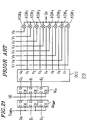
- Figure 21 shows a configuration for a part of a data driver in a prior art driving circuit.
- the circuit 210 shown in Figure 21 outputs a video signal to one of a plurality of data lines.
- the data driver requires circuits 210 the number of which is equal to the number of data lines provided in a display panel.
- video data consists of three bits (D0, D1, D2).
- the video data may have eight values of 0 to 7, and a signal voltage supplied to each pixel is one of eight levels V0-V7.
- the circuit 210 includes a sampling flip-flop M SMP , a holding flip-flop M H , a decoder DEC , and analog switches ASW0-ASW7 .
- a corresponding one of external source voltages V0-V7 of the respective eight levels which are different from each other is supplied.
- control signals S0-S7 are supplied from the decoder DEC , respectively. Each of the control signals S0-S7 is used for switching the ON/OFF state of the analog switch.
- the sampling flip-flop M SMP gets video data (D0, D1, D2), and holds the video data therein.
- an output pulse signal OE is applied to the holding flip-flop M H .
- the holding flip-flop M H gets the video data (D0, D1, D2) from the sampling flip-flop M SMP , and transfers the video data to the decoder DEC .
- the decoder DEC decodes the video data (D0, D1, D2), and produces a control signal for turning on one of the analog switches ASW0-ASW7 in accordance with the respective values (0-7) of the video data (D0, D1, D2). As a result, one of the external source voltages V0-V7 is output to a data line O n .
- the decoder DEC outputs a control signal S3 which turns on the analog switch ASW3 .
- the analog switch ASW3 becomes into the ON-state, and V3 of the external source voltages V0-V7 is output to the data line O n .
- the prior art data driver requires a large number of gray-scale voltages as the number of bits of video data increases. This causes the circuit configuration to be complicated and the circuit size to be increased. Moreover, interconnections between voltage source circuits and analog switches are also complicated.
- Figure 22 shows a configuration for a part of a driving circuit disclosed in Japanese Laid-Open Patent Publication No. 6-27900.
- the circuit 220 shown in Figure 22 outputs a video signal to one of a plurality of data lines. Accordingly, the data driver requires circuits 220 the number of which is equal to the number of data lines provided in a display panel. It is herein assumed that video data consists of 6 bits (D0, D1, D2, D3, D4, D5).
- the video data may have 64 values of 0-63, and a signal voltage applied to each pixel is one of nine gray-scale voltages V0, V8, V16, V24, V32, V40, V48, V56, and V64, and a plurality of interpolated voltages which are produced from the gray-scale voltages V0, V8, V16, V24, V32, V40, V48, V56, and V64.
- the circuit 220 includes a sampling flip-flop M SMP , a holding flip-flop M H , a selection control circuit SCOL , and analog switches ASW0-ASW8 .
- a corresponding one of gray-scale voltages V0, V8, V16, V24, V32, V40, V48, V56, and V64 of respective levels which are different from each other is supplied.
- control signals S0, S8, S16, S24, S32, S40, S48, S56, and S64 are supplied from the selection control circuit SCOL , respectively. Each of the control signals are used to switch the ON/OFF state of the analog signal.
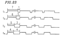
- clock signals t1, t2, t3, and t4 are supplied to the selection control circuit SCOL . As is shown in Figure 23 , the clock signals t1, t2, t3, and t4 have duty ratios which are different from each other.
- the selection control circuit SCOL receives 6-bit video data d5, d4, d3, d2, d1, and d0, and outputs one of control signals S0, S8, S16, S24, S32, S40, S48, S56, and S64 in accordance with the value of the received video data.
- the relationship between the input and the output of the selection control circuit SCOL is determined by using a logical table.
- Table 1 shows a logical table for the selection control circuit SCOL .
- the 1st to 6th columns of Table 1 indicate values of bits d5, d4, d3, d2, d1, and d0 of the video data, respectively.
- the 7th to 15th columns of Table 1 indicate values of control signals S0, S8, S16, S24, S32, S40, S48, S56, and S64, respectively.
- Each blank in the 7th to 15th columns in Table 1 means that the value of the control signal is 0.
- "t i " indicates that the value of the control signal is 1 when the value of the clock signal t i is 1, and the value of the control signal is 0 when the value of the clock signal t i is 0.
- t i -bar indicates that the value of the control signal is 0 when the value of the clock signal t i is 1, and the value of the control signal is 1 when the value of the clock signal t i is 0.
- i 1, 2, 3, and 4.
- the notation 'X-bar' is equivalent to the notation in which 'X' is provided with an upper horizontal bar. Note that 'X' is an arbitrarily selected symbol.
- Equation 1 The following equations are logical equations which define the relationships among the video data d5, d4, d3, d2, d1, and d0, the clock signals t1, t2, t3, and t4, and the control signals S0, S8, S16, S24, S32, S40, S48, S56, and S64 shown in Table 1.
- control signals S24, S32, S40, and S48 are defined.
- the control signals S56 and S64 are defined as follows.
- S56 ⁇ 49 ⁇ "t1" + ⁇ 50 ⁇ "t2" + ⁇ 51 ⁇ "t3" + ⁇ 52 ⁇ "t4" + ⁇ 53 ⁇ t3 + ⁇ 54 ⁇ t2 + ⁇ 55 ⁇ t1 + ⁇ 56 ⁇ + ⁇ 57 ⁇ t1 + ⁇ 58 ⁇ t2 + ⁇ 59 ⁇ t3 + ⁇ 60 ⁇ t4 + ⁇ 61 ⁇ "t3" + ⁇ 62 ⁇ "t2" + ⁇ 63 ⁇ "t1”
- S64 ⁇ 57 ⁇ "t1" + ⁇ 58 ⁇ "t2" + ⁇ 59 ⁇ "t3" + ⁇ 60 ⁇ "t4" + ⁇ 61 ⁇ t3 + ⁇ 62 ⁇ t2 + ⁇ 63 ⁇ t1
- ⁇ i ⁇ indicates a value when the binary data (d5, d4, d3, d2, d1, d0) is represented in the decimal notation.
- t i indicates a signal which is inverted from the signal t i .
- the selection control circuit SCOL is constructed by the logical circuits shown in Figures 24 and 25 .
- the logical circuit shown in Figure 24 produces 64 kinds of gray-scale selection data ⁇ 0 ⁇ - ⁇ 63 ⁇ in accordance with the value of 6-bit video data (d5, d4, d3, d2, d1, d0).
- the logical circuit shown in Figure 25 produces control signals S0, S8, S16, S24, S32, S40, S48, S56, and S64, based on the gray-scale selection data ⁇ 0 ⁇ - ⁇ 63 ⁇ and the clock signals t1, t2, t3, and t4.
- the video data (d5, d4, d3, d2, d1, d0) (0, 0, 0, 0, 1) is input to the selection control circuit SCOL is explained.
- the logical circuit shown in Figure 24 outputs the gray-scale selection data ⁇ 1 ⁇ .
- the logical circuit shown in Figure 25 receives the gray-scale selection data ⁇ 1 ⁇ and alternately outputs the control signal S0 and the control signal S8 at a duty ratio of the clock signal t1.
- the gray-scale voltage V0 and the gray-scale voltage V8 are alternately output via the analog switch ASW0 and the analog switch ASW1 at the duty ratio of the clock signal t1 to the data line O n .
- the actual data driver requires the selection control circuits SCOL the number of which is equal to the number of data lines.
- the circuit scale of the selection control circuit SCOL largely affects the chip size of the integrated circuit (LSI) on which the data driver is installed. If the circuit scale of the selection control circuit SCOL becomes large, the cost for the integrated circuit is increased. Moreover, if the number of bits of video data increases in order to realize an image of high resolution, the circuit scale of the data driver is further increased. This also increases the size and the production cost of the integrated circuit.
- the driving circuit of the invention is used for driving a display apparatus which includes pixels and data lines for applying voltages to the pixels and which displays an image with multiple gray scales in accordance with video data consisting of a plurality of bits.
- the driving circuit includes: oscillating signal generating means for receiving a plurality of original oscillating signals and for generating an oscillating signal T from the plurality of original oscillating signals in accordance with a value represented by bits selected from the plurality of bits of the video data; inversion means for producing an oscillating signal T-bar by inverting the oscillating signal T; gray-scale voltage specifying means for producing gray-scale voltage specifying signals which specify a first gray-scale voltage and a second gray-scale voltage among a plurality of gray-scale voltages supplied from gray-scale voltage supply means, in accordance with a value represented by bits other than the selected bits of the plurality of bits of the video data; and output means for outputting the first gray-scale voltage and the second gray-scale voltage specified by the gray-scale voltage specifying signals to
- the first gray-scale voltage and the second gray-scale voltage are adjacent ones of the plurality of gray-scale voltages.
- the plurality of oscillating signals have respective duty ratios which are different from each other.
- At least one of the plurality of oscillating signals is an inverted signal which is obtained by inverting another one of the plurality of oscillating signals.
- the plurality of oscillating signals include oscillating signals having duty ratios of 8:0, 7:1, 6:2, 5:3, 4:4, 3:5, 2:6, and 1:7, respectively.
- the video data consists of (x+y) bits, where each of x and y is a positive integer
- the gray-scale voltage specifying means produces (2 x +1) kinds of gray-scale voltage specifying signals for specifying 2 x pairs of a first gray-scale voltage and a second gray-scale voltage among the plurality of gray-scale voltages
- the oscillating signal generating means generates 2 y kinds of oscillating signals T, whereby (2 y -1) intermediate voltages of levels different from each other are generated between the first gray-scale voltage and the second gray-scale voltage specified by the gray-scale voltage specifying means, thereby displaying an image with 2 (x+y) gray scales.
- the number of the plurality of original oscillating signals is equal to the number of the selected bits among the plurality of bits of the video data.
- a driving circuit used for driving a display apparatus which includes pixels and data lines for applying voltages to the pixels and which displays an image with multiple gray scales in accordance with video data consisting of a plurality of bits.
- the driving circuit includes: control signal generating means for generating a plurality of control signals in accordance with video data consisting of a plurality of bits; and a plurality of switching means, each of the plurality of switching means being supplied with a corresponding one of the plurality of control signals and a corresponding one of a plurality of gray-scale voltages generated by gray-scale voltage generating means, the gray-scale voltage supplied to the switching means being output to the data lines via the switching means in accordance with the control signal supplied to the switching means, wherein the control signal generating means includes: oscillating signal generating means for receiving a plurality of original oscillating signals and for generating an oscillating signal T from the plurality of original oscillating signals in accordance with a value represented by bits selected from the plurality of bits of
- the first gray-scale voltage and the second gray-scale voltage are adjacent ones of the plurality of gray-scale voltages.
- At least one of the plurality of oscillating signals is an inverted signal which is obtained by inverting another one of the plurality of oscillating signals.
- the plurality of oscillating signals include oscillating signals having duty ratios of 8:0, 7:1, 6:2, 5:3, 4:4, 3:5, 2:6, and 1:7, respectively.
- the video data consists of (x+y) bits, where each of x and y is a positive integer
- the gray-scale voltage specifying means produces (2 x +1) kinds of gray-scale voltage specifying signals for specifying 2 x pairs of a first gray-scale voltage and a second gray-scale voltage among the plurality of gray-scale voltages
- the oscillating signal generating means generates 2 y kinds of oscillating signals T, whereby (2 y -1) intermediate voltages of levels different from each other are generated between the first gray-scale voltage and the second gray-scale voltage specified by the gray-scale voltage specifying means, thereby displaying an image with 2 (x+y) gray scales.
- the number of original oscillating signals is equal to the number of the selected bits of the plurality of bits of the video data.
- the switching means is an analog switch.
- a display apparatus displays an image with multiple gray scales in accordance with video data consisting of a plurality of bits.
- the display apparatus includes a display section having a plurality of pixels arranged in a matrix and a plurality of data lines for applying voltages to the plurality of pixels, and a driving circuit for driving the display section.
- the driving circuit includes oscillating signal specifying means, gray-scale voltage specifying means, and output means.
- the oscillating signal specifying means specifies one of a plurality of oscillating signals having mean values different from each other, in accordance with a value represented by bits selected from a plurality of bits of the video data.
- the gray-scale voltage specifying means specifies a pair of gray-scale voltages from a plurality of gray-scale voltages, in accordance with a value represented by the remaining bits other than the above-selected bits.
- the output means outputs oscillating voltages which oscillate between the pair of gray-scale voltages to data lines, based on the specified oscillating signal and the specified pair of gray-scale voltages. Accordingly, it is possible to realize a plurality of interpolated gray scales between the gray scales corresponding to the plurality of given gray-scale voltages.
- the plurality of oscillating signals may alternatively be generated by combining a predetermined number of oscillating signals. By reducing the number of oscillating signals, the scale of the driving circuit can be reduced.
- the driving circuit of the invention by using the gray-scale voltage specifying means and the oscillating signal specifying means, it is possible to design a logical circuit in the same manner in both cases where the driving circuit directly outputs one of the plurality of gray-scale voltages and where the driving circuit alternately outputs the specified pair of gray-scale voltages.
- the invention described herein makes possible the advantage of providing a driving circuit for a display apparatus, which has a simplified and small construction, and which can display an image with multiple gray scales in accordance with multi-bit video data.
- Figure 1 is a diagram showing the construction of a liquid crystal display apparatus.
- Figure 2 is a timing diagram illustrating the relationship among input data, sampling pulses, and an output pulse in one horizontal period.
- Figure 3 is a timing diagram illustrating the relationship among input data, an output pulse, an output voltage, and a gate pulse in one vertical period.
- Figure 4 is a timing diagram illustrating the relationship among input data, an output pulse, an output voltage, a gate pulse, and a voltage applied to a pixel in one vertical period.
- Figure 5 is a waveform chart of an output voltage oscillating in one output period.
- Figure 6 is a diagram showing a part of a configuration for a data driver in a driving circuit in Example 1 according to the invention.
- Figure 7 is a diagram showing a part of a configuration for a selection control circuit SCOL in the driving circuit in Example 1 according to the invention.
- Figure 8 is a diagram showing another part of the configuration of the selection control circuit SCOL in the driving circuit in Example 1 according to the invention.
- Figure 9 is a diagram showing another part of the configuration of the selection control circuit SCOL in the driving circuit in Example 1 according to the invention.
- Figure 10 is a diagram showing another part of the configuration of the selection control circuit SCOL in the driving circuit in Example 1 according to the invention.
- Figure 11 is a diagram showing a part of a configuration for a data driver in a driving circuit in Example 2 according to the invention.
- Figure 12 is a diagram showing a configuration of an oscillating signal generation circuit in the driving circuit in Example 2 according to the invention.
- Figure 13 is a waveform chart of oscillating signals used by the oscillating signal generation circuit.
- Figure 14 is a waveform chart of oscillating signals generated by the oscillating signal generation circuit.
- Figure 15 is a diagram showing a part of a configuration of a selection control circuit SCOL in the driving circuit in Example 2 according to the invention.
- Figure 16 is a diagram showing another part of the configuration of the selection control circuit SCOL in the driving circuit in Example 2 according to the invention.
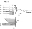
- Figure 17 is a diagram showing the configuration of an oscillating signal generation circuit in a driving circuit in Example 3 according to the invention.
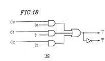
- Figure 18 is a diagram showing the configuration of an oscillating signal generation circuit in a driving circuit for 6 bits according to the invention.
- Figure 19 is a diagram showing a part of a configuration of a selection control circuit SCOL in the driving circuit for 6 bits according to the invention.
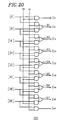
- Figure 20 is a diagram showing another part of the configuration of the selection control circuit SCOL in the driving circuit for 6 bits according to the invention.
- Figure 21 is a diagram showing a part of a configuration for a data driver in a conventional driving circuit.
- Figure 22 is a diagram showing a part of a configuration of a data driver in a driving circuit of a related art.
- Figure 23 is a waveform chart of signals t1-t4 supplied to a selection control circuit SCOL in a conventional driving circuit.
- Figure 24 is a diagram showing a part of a configuration of a selection control circuit SCOL in a conventional driving circuit.
- Figure 25 is a diagram showing another part of the configuration of a selection control circuit SCOL in a conventional driving circuit.
- a matrix type liquid crystal display apparatus is used as an example of a display apparatus. It is appreciated that the present invention is also applicable to other types of display apparatus.
- FIG 1 shows a construction of a matrix type liquid crystal display apparatus.
- the liquid crystal display apparatus shown in Figure 1 includes a display section 100 for displaying a video image, and a driving circuit 101 for driving the display section 100 .
- the driving circuit 101 includes a data driver 102 which provides video signals to the display section 100 and a scanning driver 103 which provides scanning signals to the display section 100 .
- the data driver may be called “a source driver” or "a column driver”.
- the scanning driver may be called "a gate driver” or "a row driver”.
- the display section 100 includes an M x N array of pixels 104 (M pixels in each column and N pixels in each row; where M and N are positive integers), and also includes switching elements 105 respectively connected to the pixels 104 .
- the switching elements 105 thin film transistors (TFTs) can be used. Alternatively, other types of switching elements may also be used.
- the data line may be called “a source line” or "a column line”.
- the scanning line may be called "a gate line” or "a row line”.
- the scanning driver 103 sequentially outputs a voltage which is kept at a high level during a specific time period from its output terminals G(j) to the corresponding scanning lines 107 .
- the specific time period is referred to as one horizontal period jH (where j is an integer of 1 to M).
- the total length of time obtained by adding up all the horizontal periods jH (i.e., 1H + 2H + 3H + ... + MH), a blanking period and a vertical synchronizing period is referred to as one vertical period.
- the switching element 105 connected to the output terminal G(j) When the level of the voltage which is output from the output terminal G(j) of the scanning driver 103 to the scanning line 107 is high, the switching element 105 connected to the output terminal G(j) is in the ON-state. When the switching element 105 is in the ON-state, the pixel 104 connected to the switching element 105 is charged in accordance with the voltage which is output from the output terminal S(i) of the data driver 102 to the corresponding data line 106 . The voltage of the thus charged pixel 104 remains unchanged for about one vertical period until it is charged again by the subsequent voltage to be supplied from the data driver 102 .
- Figure 2 shows the relationship among digital video data DA, sampling pulses T smpi , and an output pulse signal OE, during the jth horizontal period jH determined by a horizontal synchronizing signal H syn .
- sampling pulses T smp1 , T smp2 , ... T smpi , ..., and T smpN are sequentially applied to the data driver 102
- digital video data DA1, DA2 ..., DA i ..., and DA N are fed into the data driver 102 accordingly.
- the jth output pulse OE j determined by the output pulse signal OE is then applied to the data driver 102 .
- the data driver 102 On receiving the jth output pulse OE j , the data driver 102 outputs voltages from its output terminals S(i) to the corresponding data lines 106 .
- Figure 3 shows the relationship among the horizontal synchronizing signal H syn , the digital video data DA, the output pulse signal OE, and the output timing of the data driver 102 and the output timing of the scanning driver 103 , during one vertical period determined by a vertical synchronizing signal V syn .
- a SOURCE(j) indicates a level range of voltages output from the data driver 102 , with such timing as shown in Figure 2 and in accordance with the digital video data applied during the horizontal period jH.
- the SOURCE(j) is shown as a hatched rectangular area to indicate a level range of voltages output from all the N output terminals S(1) to S(N) of the data driver 102 .
- the voltage which is output from the jth output terminal G(j) of the scanning driver 103 to the jth scanning line 107 is changed to and kept at a high level, thereby turning on all the N switching elements 105 connected to the jth scanning line 107 .
- the N pixels 104 respectively connected to these N switching elements 105 are charged in accordance with the voltage applied to the corresponding data lines 106 from the data driver 102 .
- the above-described process is repeated M times, i.e., for the 1st to Mth scanning lines 107 , so that an image corresponding to one vertical period is displayed.
- the produced image serves as a complete display image on the display screen thereof.
- the time interval between the jth output pulse OE j and the (j+1)th output pulse OE j+1 in the output pulse signal OE is defined as "one output period". This means that one output period is equal to a period represented by SOURCE(j) shown in Figure 3 . In cases where usual line sequential scanning is performed, one output period is made equal to one horizontal period. The reason for this is as follows. While the data driver 102 outputs voltages corresponding to digital video data for one horizontal (scanning) line, to the data lines 106 , it also performs sampling of digital video data for the next horizontal line. The maximum allowable length of time during which these voltages can be output from the data driver 102 is equal to one horizontal period.
- one output period is assumed to be equal to one horizontal period. According to the present invention, however, one output period is not necessarily required to be equal to one horizontal period.
- Figure 5 shows an exemplary waveform for a voltage signal output from the data driver 102 to the data lines 106 in one output period.
- the voltage level of the voltage signal output to the data lines 106 is constant during one output period.
- the voltage signal output to the data lines 106 includes an oscillating component which oscillates during one output period.
- the voltage signal is a pulse-like signal, and a ratio of a high-level period to a low-level period, i.e., a duty ratio n:m is selected as described below.
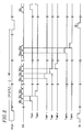
- Figure 6 shows a configuration for a part of the data driver 102 in the driving circuit 101 .
- the circuit 60 shown in Figure 6 outputs a video signal from an nth output terminal S(n) to one data line 106 .
- the data driver 102 includes circuits 60 the number of which is equal to the number of the data lines 106 provided in the display section 100 .
- the video data consists of 6 bits (D0, D1, D2, D3, D4, D5).
- the video data may have 64 kinds of values of 0 - 63, and the voltage applied to each pixel is one of nine gray-scale voltages V0, V8, V16, V24, V32, V40, V48, V56, and V64, or interpolated voltages which are produced from any pair of the gray-scale voltages chosen from V0, V8, V16, V24, V32, V40, V48, V56, and V64.
- the circuit 60 includes a sampling flip-flop M SMP which performs the sampling operation, a holding flip-flop M H which performs the holding operation, a selection control circuit SCOL , and analog switches ASW0-ASW8 .
- a corresponding one of nine gray-scale voltages V0, V8, V16, V24, V32, V40, V48, V56, and V64 is supplied.
- the gray-scale voltages V0-V64 have respective levels which are different from each other.
- the selection control circuit SCOL is supplied with seven oscillating signals t1-t7.
- the oscillating signals t1-t7 have respective duty ratios which are different from each other.
- sampling flip-flop M SMP and the holding flip-flop M H for example, D-type flip-flops can be used. It is appreciated that such sampling and holding flip-flops can be realized by using other types of circuit elements.
- the sampling flip-flop M SMP gets video data (D0, D1, D2, D3, D4, D5), and holds the video data therein.
- an output pulse signal OE is applied to the holding flip-flop M H .
- the video data held in the sampling flip-flop M SMP is fed into the holding flip-flop M H and output to the selection control circuit SCOL .
- the selection control circuit SCOL receives the video data, and produces a plurality of control signals in accordance with the value of the video data.
- the control signals are used for switching the ON/OFF states of the respective analog switches ASW0-ASW8 .
- the video data input to the selection control circuit SCOL is represented by d0, d1, d2, d3, d4, and d5, and the control signals output from the selection control circuit SCOL are represented by S0, S8, S16, S24, S32, S40, S48, S56, and S64.
- Table 2 is a logical table for the lower three bits d2, d1, and d0 of the 6-bit video data.
- the 1st to 3rd columns of Table 2 indicate the values of video data bits d2, d1, and d0, respectively.
- the oscillating signals t0-t7 are clock signals having duty ratios of 8:0, 7:1, 6:2, 5:3, 4:4, 3:5, 2:6, and 1:7, respectively.
- an oscillating signal has a duty ratio of k:0 or 0:k (k is a natural number)
- the oscillating signal is defined as always being at a fixed level.
- the oscillating signals t5, t6, and t7 are the signals obtained by inverting the oscillating signals t3, t2, and t1.
- Equation (6) can alternatively be represented as the following equation.
- T (0) + (1)t1 + (2)t2 + (3)t3 + (4)t4 + (5)t5 + (6)t6 + (7)t7
- Table 3 is a logical table representing the relationships among the upper three bits d5, d4, and d3 of the 6-bit video data, and the control signals S0, S8, S16, S24, S32, S40, S48, S56, and S64.
- a variable T denotes a signal T which is defined by Equation (6) or (7).
- a variable T-bar denotes an inverted signal T-bar obtained by inverting the signal T.
- [i] may be a value of logic-0 or logic-1
- j is a value of binary data (d5, d4, d3) which is represented in a decimal notation.
- i (8 x j)
- [i] logic-l
- [i] logic-0.
- [8] "d5" ⁇ "d4" ⁇ d3.
- T denotes an inverted signal of the signal T.
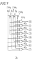
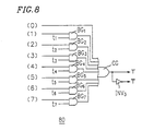
- logical circuits 70 , 80 , 90 , and 95 shown in Figures 7 through 10 are obtained.
- the selection control circuit SCOL is constructed, for example, by the logical circuits 70 , 80 , 90 , and 95 shown in Figures 7 through 10 .
- the logical circuit 70 shown in Figure 7 selectively outputs oscillating signal specifying signals (0)-(7) for specifying one of a plurality of oscillating signals t0-t7, in accordance with the lower 3 bits d2, d1, and d0 of the video data. More specifically, the video data d2, d1, and d0 and the inverted signals which are respectively obtained by inverting the video data d2, d1, and d0 by inverter circuits INV0 , INV1 , and INV2 are input into AND circuits AG0-AG7 in such combinations that constitute 0-7 in binary notation. The oscillating signal specifying signals (0)-(7) are thus obtained as the outputs of the AND circuits AG0-AG7 .
- the logical circuit 80 shown in Figure 8 specifies one of the plurality of oscillating signals t0-t7 in accordance with the oscillating signal specifying signals, and produces the specified oscillating signal T and the inverted oscillating signal T-bar which is obtained by inverting the specified oscillating signal T by an inverter circuit INV3 . More specifically, the oscillating signal specifying signals (0)-(7) and the oscillating signals t1-t7 are input into AND circuits BG1-BG7 , respectively, as is shown in Figure 8 . The outputs of the AND circuits BG1-BG7 are supplied to an OR circuit CG . The oscillating signal T and the inverted oscillating signal T-bar are obtained as the output of the OR circuit CG .
- the logical circuit 90 shown in Figure 9 selectively outputs gray-scale voltage specifying signals [0], [8], [16], [24], [32], [40], [48], and [56] for specifying a pair of gray-scale voltages from among a plurality of gray-scale voltages, in accordance with the upper three bits d5, d4, and d3 of the video data. More specifically, the video data d5, d4, and d3 and the inverted signals which are respectively obtained by inverting the video data d5, d4, and d3 by inverter circuits INV6 , INV5 , and I NV4 are input to AND circuits DG0-DG7 in such combinations which constitute 0-7 in the binary notation. As the outputs of the AND circuits DG0-DG7 , the gray-scale voltage specifying signals [0], [8], [16], [24], [32], [40], [48], and [56] are obtained.
- the logical circuit 95 shown in Figure 10 selectively outputs the control signals S0-S64, in accordance with the gray-scale voltage specifying signals [0], [8], [16], [24], [32], [40], [48], and [56], the oscillating signal T, and the inverted oscillating signal T-bar. More specifically, the gray-scale voltage specifying signals [0], [8], [16], [24], [32], [40], [48], and [56], and the oscillating signal T are input into AND circuits EG0, EG2, EG4, EG6, EG8, EG10 , EG12 , and EG14 , respectively.
- the gray-scale voltage specifying signals [0], [8], [16], [24], [32], [40], [48], and [56] and the inverted oscillating signal T-bar are input into AND circuits EG1, EG3, EG5, EG7 , EG9, EG11, EG13 , and EG15 , respectively.
- the outputs of the AND circuits EG1 and EG2 are coupled to the inputs of an OR circuit FG1 , respectively.
- the outputs of the AND circuits EG3 and EG4 are coupled to the inputs of an OR circuit FG2 , respectively.
- the outputs of the AND circuits EG5 and EG6 are coupled to an OR circuit FG3 , respectively.
- the outputs of the AND circuits EG7 and EG8 are coupled to the inputs of an OR circuit FG4 , respectively.
- the outputs of the AND circuits EG9 and EG10 are coupled to the inputs of an OR circuit FG5 , respectively.
- the outputs of the AND circuits EG11 and EG12 are coupled to the inputs of an OR circuit FG6 , respectively.
- the outputs of the AND circuits EG13 and EG14 are coupled to the inputs of an OR circuit FG7 , respectively.
- the control signals S0, S8, S16, S24, S32, S40, S48, S56, and S64 are obtained.
- the control signals S0, S8, S16, S24, S32, S40, S48, S56, and S64 are supplied to the corresponding analog switches ASW0-ASW8 .
- Each of the control signals S0, S8, S16, S24, S32, S40, S48, S56, and S64 has either a high-level value or a low-level value. For example, if the control signal is at a high level, the corresponding analog switch is controlled to be in the ON-state. If the control signal is at a low level, the corresponding analog switch is controlled to be in the OFF-state. Alternatively, the relationship between the level of the control signal and the ON/OFF state of the analog signal can be set in a reverse manner.
- a waveform of an oscillating voltage is specified in accordance with video data consisting of at least one bit selected from the plurality of bits. Then, in accordance with video data consisting of bits other than the above selected bit(s), a pair of gray-scale voltages are specified from a plurality of gray-scale voltages. As a result, a voltage signal of an appropriate level can be output for every value of video data.
- the oscillating voltage is used for realizing a plurality of interpolated gray-scale voltages between the specified pair of gray-scale voltages which are specified from among the plurality of gray-scale voltages.
- the duty ratio n:m of the oscillating signal or the control signal is interpreted to be k:0 or 0:k (k is a natural number).
- the specified pair of gray-scale voltages among the plurality of gray-scale voltages may be alternately output.
- the selection control circuit SCOL according to the invention constructed of the logical circuits 70 , 80 , 90 , and 95 shown in Figures 7 through 10 has a simplified construction as compared with the conventional selection control circuit SCOL shown in Figure 22 which is constructed of the logical circuits shown in Figures 24 and 25 .
- the oscillating signals t5-t7 are the signals inverted from the oscillating signals t1-t3. Therefore, by inverting the oscillating signals t1-t3, the oscillating signals t5-t7 are obtained in the inside of the selection control circuit SCOL . In such a case, it is sufficient to supply only the oscillating signals t1-t4 to the selection control circuit SCOL . Thus, it is possible to reduce the number of lines for supplying the oscillating signals to the selection control circuit SCOL .
- the actual data driver requires selection control circuits SCOL the number of which is equal to the number of data lines.
- the circuit scale of the selection control circuits SCOL largely affects the chip size of an integrated circuit (LSI) on which a data driver is installed.
- LSI integrated circuit
- the production cost of the integrated circuit can be decreased.
- the number of bits of video data is increased in order to realize an image of high resolution
- miniaturization of the circuit scale of the data driver is of great use. Accordingly, it is possible to make further progress in the size and cost reduction of the integrated circuit.
- a pair of gray-scale voltages are specified from the plurality of gray-scale voltages, based on the upper three bits D5, D4, and D3 of the 6-bit video data D0, D1, D2, D3, D4, and D5.
- a pair of analog switches corresponding to the specified pair of gray-scale voltages are driven at a duty ratio corresponding to the lower three bits D2, D1, and D0.
- the invention is not limited to this manner.
- the present invention can be applied to a driving circuit for driving a display apparatus in accordance with (x+y) bits.
- the display apparatus displays an image with 2 (x+y) gray scales.
- x and y are desired positive integers.
- a pair of gray-scale voltages among a plurality of gray-scale voltages are specified, based on a value represented by the upper x bits.
- the required number of gray-scale voltages is (2 x +1), and a gray-scale voltage pair is specified from 2 x gray-scale voltage pairs.
- a pair of analog switches corresponding to the specified gray-scale voltages are driven at a duty ratio corresponding to a value represented by the lower y bits.
- 2 y -1) intermediate voltages can be obtained. Therefore, the number of obtainable intermediate voltage is 2 x (2 y -1).
- the mean values of these intermediate voltages are different from each other.
- x and y are selected to be 3 and 3, respectively. This is identical with the above described example.
- a pair of analog switches corresponding to the specified pair of gray-scale voltages are driven at a duty ratio corresponding to a value represented by the lower three bits.
- x and y are selected to be 3 and 5, respectively.
- a pair of analog switches corresponding to the specified pair of gray-scale voltages are driven at a duty ratio corresponding to a value represented by the lower five bits.
- the oscillating signals t5-t7 are obtained by inverting the oscillating signals t1-t3, so that it is sufficient to supply only four oscillating signals t1-t4 to the selection control circuit SCOL .
- the required number of oscillating signals also increases. This results in the increase in number of lines for supplying the oscillating signals to the selection control circuit SCOL . For example, when the video data is composed of 8 bits, 31 oscillating signals t1-t31 are required. Even if the inverted signals are utilized, 16 oscillating signals t1-t16 are required.
- the aim of the driving circuit of this example is to reduce the number of oscillating signals.
- the configuration of the driving circuit of this example will be described.
- FIG 11 shows the configuration of a circuit corresponding to one output of an 8-bit data driver.
- the configuration is similar to that of the circuit 60 shown in Figure 6 , so that the detailed description thereof is omitted.
- oscillating signals t0-t4 are supplied to the selection control circuit SCOL . These oscillating signals may be generated in the driving circuit or may be input from the outside of the driving circuit.
- the selection control circuit SCOL has an oscillating signal generation circuit for combining a required number of oscillating signals based on the oscillating signals t0-t4.
- FIG 12 shows the configuration of the oscillating signal generation circuit 120 .
- the oscillating signal generation circuit 120 includes AND circuits FG0-FG4 and an OR circuit FG5 .
- the AND circuits FG0-FG4 receive the lower five bits (d0, d1, d2, d3, d4) of the 8-bit video data, respectively.
- the AND circuits FG0-FG4 also receive the oscillating signals t0-t4, respectively.
- the outputs of the AND circuits FG0-FG4 are coupled to the inputs of the OR circuit FG5 . With this configuration, the oscillating signal (t0-t4) can pass through the corresponding AND circuit ( FG0-FG4 ), only when the received bit is 1.
- the oscillating signals passed through the AND circuits FG0-FG4 are logically added to each other by the OR circuit FG5 .
- the output of the OR circuit FG5 is an oscillating signal T.
- an inverted oscillating signal T-bar is obtained by an inverter INV5 .
- Each of the oscillating signals t0-t4 is either a high-level value or a low-level value.
- the oscillating signals t0-t4 are required to satisfy the following conditions.
- Figure 13 shows exemplary waveforms of the oscillating signals t0-t4.
- the oscillating signals t0-t4 correspond to the lower five bits d0-d4 of the 8-bit video data, respectively.
- the lower five bits d0-d4 correspond to 20-24, respectively. Accordingly, the lengths of the high-level periods of the oscillating signals t0-t4 in one cycle are weighted in accordance with 20-24.
- the mean values of the oscillating signals t0-t4 in one cycle are 1/32, 2/32, 4/32, 8/32, and 16/32, respectively, assuming that, if the signal is kept at the high level in one cycle, the mean value of the signal is 1.
- the oscillating signal generation circuit By combining the oscillating signal t0-t4 in accordance with a value represented by the lower five bits d0-d4, the oscillating signal generation circuit generates oscillating signals T having respective mean values corresponding to values represented by the lower five bits d0-d4. As described above, the oscillating signals t0-t4 are used as bases for generating a plurality of oscillating signals T. In this specification, the oscillating signals t0-t4 are referred to as "original oscillating signals".
- Figure 14 shows waveforms of oscillating signals T generated by the oscillating signal generation circuit, in accordance with the value represented by the lower five bits d0-d4.
- oscillating signals t0-t4 by combining the oscillating signals t0-t4, oscillating signals with mean values in one cycle which are substantially equal to 0/32, 1/32, 2/32, 3/32, ⁇ , 28/32, 29/32, 30/32, 31/32.
- the signal which is kept at the low level in one cycle is regarded as an oscillating signal having a mean value of 0/32 in one cycle.
- the configuration of the oscillating signal generation circuit is not limited to that shown in Figure 12 .
- the oscillating signal generation circuit can have a desirably selected circuit configuration, so far as the oscillating signal generation circuit is a logical circuit satisfying the following logical equation (17).
- T d0t0 + d1t1 + d2t2 + d3t3 + d4t4
- Table 4 is a logical table showing the relationship among the upper three bits d7, d6, d5 of the 8-bit video data, and the control signals S0, S32, S64, S96, S128, S160, S192, S224 and S256 output from the selection control circuit SCOL .
- a variable T denotes a signal T defined by equation (17).
- a variable T-bar is an inverted signal T-bar obtained by inverting the signal T.
- the operation of the selection control circuit SCOL can be expressed in one simplified logical table, as compared with the conventional case.
- [i] is either a value of logic-0 or logic-1
- j is a value of binary data (d7, d6, d5) which is represented in a decimal notation.
- [i] logic-l
- [i] logic-0.
- [32] "d7" ⁇ "d6" ⁇ d5.
- T denotes an inverted signal of the signal T.
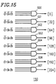
- logical circuits 150 and 160 shown in Figures 15 through 16 are obtained.
- the selection control circuit SCOL is constructed, for example, by the logical circuits 120 , 150 , and 160 shown in Figures 12 , 15 , and 16 .
- the logical circuit 150 shown in Figure 15 selectively outputs gray-scale voltage specifying signals [0], [32], [64], [96], [128], [160], [192], and [224] for specifying a pair of gray-scale voltages from among a plurality of gray-scale voltages, in accordance with the upper three bits d7, d6, and d5 of the video data.
- the logical circuit 160 shown in Figure 16 selectively outputs the control signals S0-S255, in accordance with the gray-scale voltage specifying signals [0], [32], [64], [96], [128], [160], [192], and [224], the oscillating signal T, and the inverted oscillating signal T-bar. More specifically, the gray-scale voltage specifying signals [0], [32], [64], [96], [128], [160], [192], and [224], and the oscillating signal T are input into AND circuits HG1 , HG3 , HG5 , HG7 , HG9 , HG11 , HG13 , and HG15 , respectively.
- the gray-scale voltage specifying signals [0], [32], [64], [96], [128], [160], [192], and [224] and the inverted oscillating signal T-bar are input into AND circuits HG0 , HG2, HG4, HG6, HG8, HG10, HG12, and HG14 , respectively.
- the outputs of the AND circuits HG1 and HG2 are coupled to the inputs of an OR circuit IG1 , respectively.
- the outputs of the AND circuits HG3 and HG4 are coupled to the inputs of an OR circuit IG2 , respectively.
- the outputs of the AND circuits HG5 and HG6 are coupled to an OR circuit IG3 , respectively.
- the outputs of the AND circuits HG7 and HG8 are coupled to the inputs of an OR circuit IG4 , respectively.
- the outputs of the AND circuits HG9 and HG10 are coupled to the inputs of an OR circuit IG5 , respectively.
- the outputs of the AND circuits HG11 and HG12 are coupled to the inputs of an OR circuit IG6 , respectively.
- the outputs of the AND circuits HG13 and HG14 are coupled to the inputs of an OR circuit IG7 , respectively.
- the control signals S0, S32, S64, S96, S128, S160, S192, S224, and S256 are obtained.
- the control signals S0, S32, S64, S96, S128, S160, S192, S224, and S256 are supplied to the corresponding analog switches ASW0-ASW8 .
- Each of the control signals S0, S32, S64, S96, S128, S160, S192, S224, and S256 has either a high-level value or a low-level value. For example, if the control signal is at a high level, the corresponding analog switch is controlled to be in the ON-state. If the control signal is at a low level, the corresponding analog switch is controlled to be in the OFF-state. Alternatively, the relationship between the level of the control signal and the ON/OFF state of the analog signal can be set in a reverse manner. For the practical LSI, the sizes of the logical circuits 120 , 150 , and 160 can be optimized using design rules for logical circuits.
- oscillating signals having specific waveforms are generated in accordance with video data consisting of at least one bit selected from the plurality of bits, and a pair of gray-scale voltages are specified from a plurality of gray-scale voltages in accordance with video data consisting of bits other than the above-selected bit(s).
- a voltage signal of an appropriate level can be output for every value of video data.
- the oscillating voltage is used for realizing a plurality of interpolated gray-scale voltages between the specified pair of gray-scale voltages which are specified from among the plurality of gray-scale voltages.
- the driving circuit of this example it is possible to generate 31 kinds of intermediate voltages between the paired gray-scale voltages. Accordingly, 9 kinds of gray-scale voltages result in a display of an image with 256 gray scales.
- a large number of oscillating signals can be generated based on a smaller number of oscillating signals, so that it is possible to reduce the number of lines for supplying the oscillating signals to the selection control circuit.
- the driving circuit of this example has a simplified configuration, as compared with the conventional driving circuit or the driving circuit of Example 1.
- the number of the oscillating signals t0-t4 has been assumed to be equal to the number of lower bits (i.e., 5) used for specifying the oscillating signal T of the 8-bit video data.
- the invention is not limited to this specific case.
- some of the oscillating signals t0-t4 can be omitted, because the omitted oscillating signal(s) can be generated by repeatedly using the remaining oscillating signals.
- the duty ratio of the oscillating signal is not limited to the above-described example.
- the driving circuit in Example 2 outputs an oscillating voltage which oscillates between the gray-scale voltage V224 and the gray-scale voltage V256, in accordance with the video data having the maximum value of 255 which can be represented by 8 bits.
- the driving circuit in Example 2 outputs an oscillating voltage which oscillates between the gray-scale voltage V224 and the gray-scale voltage V256, in accordance with the video data having the maximum value of 255 which can be represented by 8 bits.
- intermediate voltages between the gray-scale voltage V224 and the gray-scale voltage V256 are applied to the pixel.
- Example 3 describes a driving circuit which directly outputs the gray-scale voltage V256 in accordance with the video data having the maximum value of 255 which can be represented by 8 bits.
- the configuration of the driving circuit in this example is identical with that of the driving circuit shown in Figure 11 except for the oscillating signal generation circuit.
- Equation (27) when the value of the video data is 255, the value of the variable T is 1, so that only the value of the control signal S256 is 1 on the basis of Table 4. As a result, only the analog switch ASW8 is turned ON, so that only the gray-scale voltage V256 is output. Accordingly, it is possible to clearly distinguish the gray scales in the case where the video data has the value of 255 from the gray scales in the case where the video data has the value of 254. Therefore, it is possible to increase the contrast (the maximum gray scale / the minimum gray scale) of the image displayed on the display apparatus.
- FIG 17 shows an example in which the oscillating signal generation circuit is implemented as a logical circuit.
- the configuration of the oscillating signal generation circuit is not limited to that shown in Figure 17 .
- the oscillating signal generation circuit can have any desired configuration, so far as the logical circuit satisfies the logical equation expressed as Equation (27).
- the driving circuit of this example it is possible to reduce the number of oscillating signals, as in the driving circuit of Example 2. Therefore, it is possible to reduce the number of lines for supplying the oscillating signals to the selection control circuit. Such effects are remarkably attained in cases where the invention is applied to a driving circuit for a display with multiple gray scales such as an 8-bit data driver for the following reasons.
- the 8-bit data driver necessitates 16 oscillating signals.
- the 8-bit data driver of Examples 2 and 3 only requires five oscillating signals t0-t4. These oscillating signals are required to be supplied to all of the selection control circuits provided in the data driver, so that the lines for supplying the oscillating signals to the selection control circuits are disposed over the entire LSI to which the data driver is mounted. Accordingly, the reduction of the number of lines for supplying the oscillating signals to the selection control circuits largely contributes to the miniaturization of the LSI chip.
- the oscillating signals are signals which are always operating, so that the reduction of the number of oscillating signals may result in the reduction of power consumption.
- the required number of oscillating signals is reduced from four to three.
- the data drivers of Examples 2 and 3 have at least two features.
- the first feature is that a plurality of oscillating signals are generated by a simple logic operation with respect to the original oscillating signals.
- the plurality of oscillating signals are generated by an oscillating signal generation circuit.
- the second feature is that the plurality of generated oscillating signals are used as parameters for defining the mean value of the oscillating voltage which oscillates between a pair of gray-scale voltages. Due to these features, the driving circuits of Examples 2 and 3 have an advantage in that the size of logical circuits for all of the selection control circuit can drastically be reduced. The advantage is described below in detail.
- Figures 18 , 19 , and 20 show configurations of a selection control circuit in the 6-bit data driver according to the invention.
- Table 6 shows the logical table for defining the operation of the selection control circuit.
- the configuration of the 8-bit data driver shown in Figures 12 , 15 , and 16 is compared with the configuration of the 6-bit data driver shown in Figures 18 , 19 , and 20 , it is found that they are identical with each other except for the oscillating signal generation circuit. This is because the logical table (Table 4) of the selection control circuit for 8 bits has the same format as that of the logical table (table 6) of the selection control circuit for 6 bits.
- the required number of gray-scale voltages in the selection control circuit for 8 bits is equal to the required number of gray-scale voltages in the selection control circuit for 6 bits.
- the number of gray-scale voltages is 9.
- the selection control circuit for 8 bits can be realized in the same size as that of the selection control circuit for 6 bits.
- the selection control circuit for 8 bits had the size which was at least several times as large as that of the selection control circuit for 6 bits.
- the size reduction effect for the selection control circuit according to the invention is significantly great, because the data driver has a plurality of outputs and each of the outputs requires a selection control circuit.
- the cost for the entire data driver can be greatly decreased. For example, as the result of the conventional design concept, it was difficult to provide the 8-bit data driver at a reasonable price. According to the invention, such an 8-bit data driver can be provided at a reasonable price for the first time.
- the interpolation is started with the gray scale 0 and performed from the gray scale 1.
- the interpolation may be performed in a reversed sequence.
- the interpolation is started with the gray scale 255 and performed from the gray scale 254.
- the variable T is defined so that the gray-scale voltage V0 is directly output when the value of the video data is 0.
- the invention it is possible to obtain one or more interpolated voltages from voltages supplied from given voltage sources, whereby the number of voltage sources can be greatly decreased as compared with a conventional driving circuit which requires a large number of voltage sources. If the voltage sources are provided from the outside of the driving circuit, the number of input terminals of the driving circuit can be reduced. If the driving circuit is constructed as an LSI, the number of input terminals of the LSI can be reduced. According to the invention, it is possible to realize a driving LSI for displaying an image with multiple gray scales which could not be realized by the prior art example because of the increase in the number of terminals.
- the following effects can be attained: (1) the production cost of a display apparatus and a driving circuit are largely reduced; (2) a driving circuit for multiple gray scales which could not be practically produced due to the chip size or the LSI installation can be readily produced; and (3) the power consumption is decreased because a large number of voltage sources are not required.
Landscapes
- Physics & Mathematics (AREA)
- Engineering & Computer Science (AREA)
- Nonlinear Science (AREA)
- Crystallography & Structural Chemistry (AREA)
- General Physics & Mathematics (AREA)
- Chemical & Material Sciences (AREA)
- Computer Hardware Design (AREA)
- Theoretical Computer Science (AREA)
- Microelectronics & Electronic Packaging (AREA)
- Mathematical Physics (AREA)
- Optics & Photonics (AREA)
- Control Of Indicators Other Than Cathode Ray Tubes (AREA)
- Liquid Crystal Display Device Control (AREA)
Applications Claiming Priority (3)
| Application Number | Priority Date | Filing Date | Title |
|---|---|---|---|
| JP29710393 | 1993-11-26 | ||
| JP29710393A JP2869315B2 (ja) | 1993-05-14 | 1993-11-26 | 表示装置の駆動回路 |
| JP297103/93 | 1993-11-26 |
Publications (2)
| Publication Number | Publication Date |
|---|---|
| EP0655726A1 true EP0655726A1 (de) | 1995-05-31 |
| EP0655726B1 EP0655726B1 (de) | 1999-09-08 |
Family
ID=17842253
Family Applications (1)
| Application Number | Title | Priority Date | Filing Date |
|---|---|---|---|
| EP94307896A Expired - Lifetime EP0655726B1 (de) | 1993-11-26 | 1994-10-27 | Graupegelwählende Schaltung für eine Anzeigesteuerschaltung |
Country Status (5)
| Country | Link |
|---|---|
| EP (1) | EP0655726B1 (de) |
| KR (1) | KR0150262B1 (de) |
| CN (1) | CN1080912C (de) |
| DE (1) | DE69420520T2 (de) |
| TW (1) | TW306998B (de) |
Cited By (5)
| Publication number | Priority date | Publication date | Assignee | Title |
|---|---|---|---|---|
| US6067064A (en) * | 1995-12-21 | 2000-05-23 | Hitachi, Ltd. | Liquid crystal driving circuit and liquid crystal display system using the same |
| EP1031961A2 (de) | 1999-02-24 | 2000-08-30 | Semiconductor Energy Laboratory Co., Ltd. | Gradationssteuerung für eine Anzeige |
| EP1037192A2 (de) | 1999-03-18 | 2000-09-20 | Sel Semiconductor Energy Laboratory Co., Ltd. | Graustufenansteuerung für eine Anzeigetafel mit aktiver Matrix |
| US6952194B1 (en) | 1999-03-31 | 2005-10-04 | Semiconductor Energy Laboratory Co., Ltd. | Liquid crystal display device |
| US7145536B1 (en) | 1999-03-26 | 2006-12-05 | Semiconductor Energy Laboratory Co., Ltd. | Liquid crystal display device |
Families Citing this family (2)
| Publication number | Priority date | Publication date | Assignee | Title |
|---|---|---|---|---|
| US8026888B2 (en) * | 2003-07-30 | 2011-09-27 | Tpo Hong Kong Holding Limited | Voltage supplying device |
| CN110534054B (zh) * | 2019-07-31 | 2021-06-22 | 华为技术有限公司 | 显示驱动方法及装置、显示装置、存储介质、芯片 |
Citations (5)
| Publication number | Priority date | Publication date | Assignee | Title |
|---|---|---|---|---|
| EP0171547A2 (de) * | 1984-07-13 | 1986-02-19 | Ascii Corporation | Anzeigesteuersystem |
| EP0433054A2 (de) * | 1989-12-14 | 1991-06-19 | Sharp Kabushiki Kaisha | Steuereinrichtung für ein Flüssigkristallanzeigegerät |
| EP0515191A2 (de) * | 1991-05-21 | 1992-11-25 | Sharp Kabushiki Kaisha | Verfahren und Einrichtung zum Steuern einer Anzeigeeinrichtung |
| JPH05100635A (ja) * | 1991-10-07 | 1993-04-23 | Nec Corp | アクテイブマトリクス型液晶デイスプレイの駆動用集積回路と駆動方法 |
| EP0624862A2 (de) * | 1993-05-14 | 1994-11-17 | Sharp Kabushiki Kaisha | Steuerungsverfahren für Anzeigevorrichtung |
-
1994
- 1994-10-07 TW TW083109334A patent/TW306998B/zh not_active IP Right Cessation
- 1994-10-27 EP EP94307896A patent/EP0655726B1/de not_active Expired - Lifetime
- 1994-10-27 DE DE69420520T patent/DE69420520T2/de not_active Expired - Fee Related
- 1994-11-25 KR KR1019940031614A patent/KR0150262B1/ko not_active Expired - Fee Related
- 1994-11-25 CN CN94118510A patent/CN1080912C/zh not_active Expired - Fee Related
Patent Citations (5)
| Publication number | Priority date | Publication date | Assignee | Title |
|---|---|---|---|---|
| EP0171547A2 (de) * | 1984-07-13 | 1986-02-19 | Ascii Corporation | Anzeigesteuersystem |
| EP0433054A2 (de) * | 1989-12-14 | 1991-06-19 | Sharp Kabushiki Kaisha | Steuereinrichtung für ein Flüssigkristallanzeigegerät |
| EP0515191A2 (de) * | 1991-05-21 | 1992-11-25 | Sharp Kabushiki Kaisha | Verfahren und Einrichtung zum Steuern einer Anzeigeeinrichtung |
| JPH05100635A (ja) * | 1991-10-07 | 1993-04-23 | Nec Corp | アクテイブマトリクス型液晶デイスプレイの駆動用集積回路と駆動方法 |
| EP0624862A2 (de) * | 1993-05-14 | 1994-11-17 | Sharp Kabushiki Kaisha | Steuerungsverfahren für Anzeigevorrichtung |
Non-Patent Citations (1)
| Title |
|---|
| PATENT ABSTRACTS OF JAPAN vol. 17, no. 451 (P - 1595) 18 August 1993 (1993-08-18) * |
Cited By (15)
| Publication number | Priority date | Publication date | Assignee | Title |
|---|---|---|---|---|
| US6067064A (en) * | 1995-12-21 | 2000-05-23 | Hitachi, Ltd. | Liquid crystal driving circuit and liquid crystal display system using the same |
| EP1031961A2 (de) | 1999-02-24 | 2000-08-30 | Semiconductor Energy Laboratory Co., Ltd. | Gradationssteuerung für eine Anzeige |
| EP1031961A3 (de) * | 1999-02-24 | 2001-10-31 | Semiconductor Energy Laboratory Co., Ltd. | Gradationssteuerung für eine Anzeige |
| US7233342B1 (en) | 1999-02-24 | 2007-06-19 | Semiconductor Energy Laboratory Co., Ltd. | Time and voltage gradation driven display device |
| US7714825B2 (en) | 1999-03-18 | 2010-05-11 | Semiconductor Energy Laboratory Co., Ltd. | Display device |
| EP1037192A2 (de) | 1999-03-18 | 2000-09-20 | Sel Semiconductor Energy Laboratory Co., Ltd. | Graustufenansteuerung für eine Anzeigetafel mit aktiver Matrix |
| EP1037192A3 (de) * | 1999-03-18 | 2001-01-17 | Sel Semiconductor Energy Laboratory Co., Ltd. | Graustufenansteuerung für eine Anzeigetafel mit aktiver Matrix |
| US8570263B2 (en) | 1999-03-18 | 2013-10-29 | Semiconductor Energy Laboratory Co., Ltd. | Electronic equipment including LED backlight |
| US7193594B1 (en) | 1999-03-18 | 2007-03-20 | Semiconductor Energy Laboratory Co., Ltd. | Display device |
| US7145536B1 (en) | 1999-03-26 | 2006-12-05 | Semiconductor Energy Laboratory Co., Ltd. | Liquid crystal display device |
| US8144278B2 (en) | 1999-03-26 | 2012-03-27 | Semiconductor Energy Laboratory Co., Ltd. | Optically compensated birefringence mode liquid crystal display device |
| US8896639B2 (en) | 1999-03-26 | 2014-11-25 | Semiconductor Energy Laboratory Co., Ltd. | Liquid crystal display device |
| US9704444B2 (en) | 1999-03-26 | 2017-07-11 | Semiconductor Energy Laboratory Co., Ltd. | Liquid crystal display device |
| US7333082B2 (en) | 1999-03-31 | 2008-02-19 | Semiconductor Energy Laboratory Co., Ltd. | Liquid crystal display device |
| US6952194B1 (en) | 1999-03-31 | 2005-10-04 | Semiconductor Energy Laboratory Co., Ltd. | Liquid crystal display device |
Also Published As
| Publication number | Publication date |
|---|---|
| CN1122934A (zh) | 1996-05-22 |
| DE69420520D1 (de) | 1999-10-14 |
| DE69420520T2 (de) | 2000-01-20 |
| TW306998B (de) | 1997-06-01 |
| KR950014957A (ko) | 1995-06-16 |
| EP0655726B1 (de) | 1999-09-08 |
| KR0150262B1 (ko) | 1998-10-15 |
| CN1080912C (zh) | 2002-03-13 |
Similar Documents
| Publication | Publication Date | Title |
|---|---|---|
| EP0391655B1 (de) | Ansteuerschaltung für ein Matrixanzeigegerät mit Flüssigkristallen | |
| JP3512710B2 (ja) | 液晶表示装置 | |
| US6862021B2 (en) | Liquid crystal display control apparatus and liquid crystal display apparatus | |
| EP0584114B1 (de) | Flüssigkristallanzeige | |
| EP0478386B1 (de) | Steuerschaltung für ein Anzeigegerät | |
| US6462728B1 (en) | Apparatus having a DAC-controlled ramp generator for applying voltages to individual pixels in a color electro-optic display device | |
| US5621426A (en) | Display apparatus and driving circuit for driving the same | |
| EP0515191A2 (de) | Verfahren und Einrichtung zum Steuern einer Anzeigeeinrichtung | |
| US5673061A (en) | Driving circuit for display apparatus | |
| EP0624862B1 (de) | Steuerungsverfahren für Anzeigevorrichtung | |
| EP0655726A1 (de) | Graupegelwählende Schaltung für eine Anzeigesteuerschaltung | |
| KR100806907B1 (ko) | 액정 표시 장치 및 이의 구동 방법 | |
| JPH10301545A (ja) | 液晶パネルの駆動方法、セグメントドライバ、表示コントローラ及び液晶表示装置 | |
| KR930005369B1 (ko) | 많은색의 컬러 표시방법 및 장치 | |
| JP3669514B2 (ja) | 液晶表示装置の駆動回路 | |
| KR960014499B1 (ko) | 표시장치의 구동회로 | |
| JPH07175452A (ja) | 液晶表示装置 | |
| JPH09106265A (ja) | 電圧出力回路および画像表示装置 | |
| JPH07104716A (ja) | 表示装置 | |
| JPH08114784A (ja) | 液晶表示装置 | |
| US20110157130A1 (en) | Driving method of electro optical device, driving device of electro optical device, electro optical device, and electronic instrument | |
| EP0599621B1 (de) | Steuervorrichtung für ein Anzeigegerät, die die Spannungseinstellung verbessert | |
| JPH06161391A (ja) | 液晶駆動回路 | |
| JP3549127B2 (ja) | 液晶表示装置 | |
| JP2869315B2 (ja) | 表示装置の駆動回路 |
Legal Events
| Date | Code | Title | Description |
|---|---|---|---|
| PUAI | Public reference made under article 153(3) epc to a published international application that has entered the european phase |
Free format text: ORIGINAL CODE: 0009012 |
|
| AK | Designated contracting states |
Kind code of ref document: A1 Designated state(s): DE FR GB NL |
|
| 17P | Request for examination filed |
Effective date: 19950901 |
|
| 17Q | First examination report despatched |
Effective date: 19971014 |
|
| GRAG | Despatch of communication of intention to grant |
Free format text: ORIGINAL CODE: EPIDOS AGRA |
|
| GRAG | Despatch of communication of intention to grant |
Free format text: ORIGINAL CODE: EPIDOS AGRA |
|
| GRAG | Despatch of communication of intention to grant |
Free format text: ORIGINAL CODE: EPIDOS AGRA |
|
| GRAG | Despatch of communication of intention to grant |
Free format text: ORIGINAL CODE: EPIDOS AGRA |
|
| GRAG | Despatch of communication of intention to grant |
Free format text: ORIGINAL CODE: EPIDOS AGRA |
|
| GRAH | Despatch of communication of intention to grant a patent |
Free format text: ORIGINAL CODE: EPIDOS IGRA |
|
| GRAH | Despatch of communication of intention to grant a patent |
Free format text: ORIGINAL CODE: EPIDOS IGRA |
|
| GRAA | (expected) grant |
Free format text: ORIGINAL CODE: 0009210 |
|
| AK | Designated contracting states |
Kind code of ref document: B1 Designated state(s): DE FR GB NL |
|
| REF | Corresponds to: |
Ref document number: 69420520 Country of ref document: DE Date of ref document: 19991014 |
|
| ET | Fr: translation filed | ||
| PLBE | No opposition filed within time limit |
Free format text: ORIGINAL CODE: 0009261 |
|
| STAA | Information on the status of an ep patent application or granted ep patent |
Free format text: STATUS: NO OPPOSITION FILED WITHIN TIME LIMIT |
|
| 26N | No opposition filed | ||
| REG | Reference to a national code |
Ref country code: GB Ref legal event code: IF02 |
|
| PGFP | Annual fee paid to national office [announced via postgrant information from national office to epo] |
Ref country code: FR Payment date: 20021008 Year of fee payment: 9 |
|
| PGFP | Annual fee paid to national office [announced via postgrant information from national office to epo] |
Ref country code: GB Payment date: 20021023 Year of fee payment: 9 |
|
| PGFP | Annual fee paid to national office [announced via postgrant information from national office to epo] |
Ref country code: NL Payment date: 20021031 Year of fee payment: 9 Ref country code: DE Payment date: 20021031 Year of fee payment: 9 |
|
| PG25 | Lapsed in a contracting state [announced via postgrant information from national office to epo] |
Ref country code: GB Free format text: LAPSE BECAUSE OF NON-PAYMENT OF DUE FEES Effective date: 20031027 |
|
| PG25 | Lapsed in a contracting state [announced via postgrant information from national office to epo] |
Ref country code: NL Free format text: LAPSE BECAUSE OF NON-PAYMENT OF DUE FEES Effective date: 20040501 Ref country code: DE Free format text: LAPSE BECAUSE OF NON-PAYMENT OF DUE FEES Effective date: 20040501 |
|
| GBPC | Gb: european patent ceased through non-payment of renewal fee |
Effective date: 20031027 |
|
| PG25 | Lapsed in a contracting state [announced via postgrant information from national office to epo] |
Ref country code: FR Free format text: LAPSE BECAUSE OF NON-PAYMENT OF DUE FEES Effective date: 20040630 |
|
| NLV4 | Nl: lapsed or anulled due to non-payment of the annual fee |
Effective date: 20040501 |
|
| REG | Reference to a national code |
Ref country code: FR Ref legal event code: ST |