EP0655742B1 - Integrierter Schaltkreis mit elektrisch programmier- und löschbaren Speicherzellen - Google Patents
Integrierter Schaltkreis mit elektrisch programmier- und löschbaren Speicherzellen Download PDFInfo
- Publication number
- EP0655742B1 EP0655742B1 EP93830481A EP93830481A EP0655742B1 EP 0655742 B1 EP0655742 B1 EP 0655742B1 EP 93830481 A EP93830481 A EP 93830481A EP 93830481 A EP93830481 A EP 93830481A EP 0655742 B1 EP0655742 B1 EP 0655742B1
- Authority
- EP
- European Patent Office
- Prior art keywords
- cells
- cell
- row
- memory cells
- terminal connected
- Prior art date
- Legal status (The legal status is an assumption and is not a legal conclusion. Google has not performed a legal analysis and makes no representation as to the accuracy of the status listed.)
- Expired - Lifetime
Links
Images
Classifications
-
- G—PHYSICS
- G11—INFORMATION STORAGE
- G11C—STATIC STORES
- G11C16/00—Erasable programmable read-only memories
- G11C16/02—Erasable programmable read-only memories electrically programmable
- G11C16/04—Erasable programmable read-only memories electrically programmable using variable threshold transistors, e.g. FAMOS
- G11C16/0408—Erasable programmable read-only memories electrically programmable using variable threshold transistors, e.g. FAMOS comprising cells containing floating gate transistors
- G11C16/0416—Erasable programmable read-only memories electrically programmable using variable threshold transistors, e.g. FAMOS comprising cells containing floating gate transistors comprising cells containing a single floating gate transistor and no select transistor, e.g. UV EPROM
-
- G—PHYSICS
- G11—INFORMATION STORAGE
- G11C—STATIC STORES
- G11C16/00—Erasable programmable read-only memories
- G11C16/02—Erasable programmable read-only memories electrically programmable
- G11C16/04—Erasable programmable read-only memories electrically programmable using variable threshold transistors, e.g. FAMOS
-
- G—PHYSICS
- G11—INFORMATION STORAGE
- G11C—STATIC STORES
- G11C16/00—Erasable programmable read-only memories
- G11C16/02—Erasable programmable read-only memories electrically programmable
- G11C16/06—Auxiliary circuits, e.g. for writing into memory
- G11C16/10—Programming or data input circuits
- G11C16/14—Circuits for erasing electrically, e.g. erase voltage switching circuits
- G11C16/16—Circuits for erasing electrically, e.g. erase voltage switching circuits for erasing blocks, e.g. arrays, words, groups
-
- G—PHYSICS
- G11—INFORMATION STORAGE
- G11C—STATIC STORES
- G11C16/00—Erasable programmable read-only memories
- G11C16/02—Erasable programmable read-only memories electrically programmable
- G11C16/06—Auxiliary circuits, e.g. for writing into memory
- G11C16/22—Safety or protection circuits preventing unauthorised or accidental access to memory cells
Definitions
- This invention relates to electrically programmable non-volatile storage cell devices comprising, in particular, non-erasable only time programmable (OTP) memory cells in addition to electrically erasable read/write memory cells.
- OTP non-erasable only time programmable
- Non-volatile storage devices EEPROMs, EPROMs and FLASHEEPROMs
- EEPROMs Non-volatile storage devices
- EPROMs EPROMs
- FLASHEEPROMs FLASHEEPROMs
- It may include, for example, operation speed class, any redundancy used, the manufacturing date and batch, and the like items of information.
- non-volatile storage devices comprising memory cells set up into a matrix type of architecture, wherein rows and columns of cells are to be found together with lines to interconnect cells in one row and cells in one column, it may be convenient to add, to rows driven by the row decoding facility which permits the user memory matrix to be accessed, a few rows of OTP cells in the matrix.
- These rows utilize the same circuitry as the user memory matrix for read and write operations and are enabled by appropriate signals through the row decoding facility itself.
- This kind of circuit architecture is conceptually simple and effective, but may create some even serious reliability problems with electrically erasable non-volatile storage cell devices, in particular with FLASHEEPROMs.
- the selection of the potential reference to which the sources of the OTP cells should be connected becomes a critical one.
- the underlying technical problem of this invention is to allow rows of OTP cells to be included to the memory cell matrix of an electrically erasable storage with no reliability or operation problems.
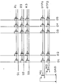
- Shown in the drawing figure is a matrix type of circuit arrangement for the memory cells included to an electrically erasable non-volatile storage device which comprises, additionally to rows of programmable and erasable user memory cells, rows of OTP memories, that is programmable and non-erasable memories, as denoted by OTP1 and OTP2.
- drain terminals of all the transistor structures of the memory cells, including the OTPs, in one column are connected to a common column selection line, D1, D2, ..., or bit line where the columns relate to bits of a word written in the memory.
- the gate terminals of all the memory cells, including the OTPs, in one row are connected to a common row decoding line R1, R2,..., OTP1 and OTP2.
- the source terminals of all the re-programmable and electrically erasable user memory cells are connected to a control line for the cell states through which the sources of such cells are either impressed the potential that determines the erase state or the potential that admits of the read or program state.
- the control line could be provided other than single where the cells are controlled by row sectors (S1, S2,).
- all the source terminals of the non-erasable OTP memory cells in one row are connected to a common line connected, in turn, to a potential reference GND, being preferably the device ground, through an electronic switch comprising a switching transistor (M1, M2).
- One transistor is required for each row of OTP cells.
- the control terminals of such transistors which are field-effect transistors as shown, are connected to the same row decoding lines for the respective rows, OTP1 and OTP2.
- the sources of those cells are brought to ground potential through the transistor operated by the decoding line. Thus, reading such cells or initially programming them is allowed.
- An outstanding advantage is that the need for additional external control signals to drive the selection transistors of the OTP cells is avoided, since the transistors are controlled from the OTP row decoding lines.
Landscapes
- Engineering & Computer Science (AREA)
- Microelectronics & Electronic Packaging (AREA)
- Computer Security & Cryptography (AREA)
- Read Only Memory (AREA)
- Non-Volatile Memory (AREA)
Claims (3)
- Monolitisch integriertes Speicherbauelement, umfassend elektrisch programmierbare, nicht flüchtige Speicherzellen, die zu einer Matrixkonfiguration aus Zellenreihen und -spalten verbunden sind, wobei jede Zelle mindestens einen ersten Anschluß, der an eine Steuerleitung (S1, S2, ...) die für die Zellen einer Reihe gemeinsam vorhanden ist, um den Zellenzustand zu steuern, angeschlossen ist, einen zweiten Anschluß der an eine Auswahlleitung (D1, D2, ...) für die die Zelle enthaltende Spalte angeschlossen ist, und einen Auswahlanschluß aufweist, der an eine Dekodierleitung (R1 - R3, OTP1, OTP2) für die die Zelle enthaltende Reihe angeschlossen ist, wobei die Zellenmatrixkonfiguration mindestens eine Reihe von elektrisch löschbaren Lese-/Schreib-Zellen und mindestens eine Reihe von nicht-löschbaren Nur-Lese-Zellen aufweist,
dadurch gekennzeichnet,
daß zwischen einem Referenzpotential (GND) und der den Zustand der nicht-löschbaren Nur-Lese-Zellen steuernden Steuerleitung ein elektronischer Schalter (M1, M2) liegt, wobei der Schalter (M1, M2) einen Steueranschluß besitzt, der an die Decodierleitung (OTP1, OTP2) für die Reihe der nicht-löschbaren Nur-Lese-Zellen angeschlossen ist. - Speicherzellenbauelement nach Anspruch 1,
dadurch gekennzeichnet,
daß der elektronische Schalter (M1, M2) ein Feldeffekttransistor ist, der mit einem Gateanschluß an die Decodierleitung (OPT1, OTP2) für die Nur-Lese-Zellen-Reihe angeschlossen ist. - Speicherzellenbauelement nach Anspruch 1 oder 2,
dadurch gekennzeichnet,
daß das Referenzpotential das Massepotential des Bauelements ist.
Priority Applications (4)
| Application Number | Priority Date | Filing Date | Title |
|---|---|---|---|
| DE1993623494 DE69323494T2 (de) | 1993-11-30 | 1993-11-30 | Integrierter Schaltkreis mit elektrisch programmier- und löschbaren Speicherzellen |
| EP93830481A EP0655742B1 (de) | 1993-11-30 | 1993-11-30 | Integrierter Schaltkreis mit elektrisch programmier- und löschbaren Speicherzellen |
| JP29488294A JP2617095B2 (ja) | 1993-11-30 | 1994-11-29 | 画一的に集積された記憶装置 |
| US08/347,653 US5535157A (en) | 1993-11-30 | 1994-11-30 | Monolithically integrated storage device |
Applications Claiming Priority (2)
| Application Number | Priority Date | Filing Date | Title |
|---|---|---|---|
| EP93830481A EP0655742B1 (de) | 1993-11-30 | 1993-11-30 | Integrierter Schaltkreis mit elektrisch programmier- und löschbaren Speicherzellen |
| US08/347,653 US5535157A (en) | 1993-11-30 | 1994-11-30 | Monolithically integrated storage device |
Publications (2)
| Publication Number | Publication Date |
|---|---|
| EP0655742A1 EP0655742A1 (de) | 1995-05-31 |
| EP0655742B1 true EP0655742B1 (de) | 1999-02-10 |
Family
ID=26134914
Family Applications (1)
| Application Number | Title | Priority Date | Filing Date |
|---|---|---|---|
| EP93830481A Expired - Lifetime EP0655742B1 (de) | 1993-11-30 | 1993-11-30 | Integrierter Schaltkreis mit elektrisch programmier- und löschbaren Speicherzellen |
Country Status (3)
| Country | Link |
|---|---|
| US (1) | US5535157A (de) |
| EP (1) | EP0655742B1 (de) |
| JP (1) | JP2617095B2 (de) |
Families Citing this family (6)
| Publication number | Priority date | Publication date | Assignee | Title |
|---|---|---|---|---|
| EP0798727B1 (de) * | 1996-03-29 | 2004-05-26 | STMicroelectronics S.r.l. | Datenleseverwaltungsarchitektur für eine Speichervorrichtung, besonders für nichtflüchtige Speicher |
| FR2771839B1 (fr) * | 1997-11-28 | 2000-01-28 | Sgs Thomson Microelectronics | Memoire non volatile programmable et effacable electriquement |
| WO2002037502A2 (en) * | 2000-10-30 | 2002-05-10 | Virtual Silicon Technology, Inc. | Common source eeprom and flash memory |
| US7777281B2 (en) * | 2004-03-26 | 2010-08-17 | Atmel Corporation | Non-volatile transistor memory array incorporating read-only elements with single mask set |
| JP5468489B2 (ja) * | 2010-07-29 | 2014-04-09 | 株式会社東芝 | 半導体記憶装置の動作方法 |
| US10090840B1 (en) * | 2017-06-29 | 2018-10-02 | Intel Corporation | Integrated circuits with programmable non-volatile resistive switch elements |
Family Cites Families (7)
| Publication number | Priority date | Publication date | Assignee | Title |
|---|---|---|---|---|
| US4698787A (en) * | 1984-11-21 | 1987-10-06 | Exel Microelectronics, Inc. | Single transistor electrically programmable memory device and method |
| JPH0734313B2 (ja) * | 1985-08-09 | 1995-04-12 | 株式会社日立製作所 | Icメモリ装置 |
| US5001670A (en) * | 1987-02-06 | 1991-03-19 | Tektronix, Inc. | Nonvolatile memory protection |
| KR890001099A (ko) * | 1987-06-08 | 1989-03-18 | 미다 가쓰시게 | 반도체 기억장치 |
| JPH022435A (ja) * | 1988-06-15 | 1990-01-08 | Seiko Instr Inc | 半導体不揮発性記憶装置 |
| JPH07114077B2 (ja) * | 1989-06-01 | 1995-12-06 | 三菱電機株式会社 | 不揮発性半導体記憶装置 |
| JPH0378195A (ja) * | 1989-08-21 | 1991-04-03 | Mitsubishi Electric Corp | Epromを内蔵したマイクロコンピュータ装置 |
-
1993
- 1993-11-30 EP EP93830481A patent/EP0655742B1/de not_active Expired - Lifetime
-
1994
- 1994-11-29 JP JP29488294A patent/JP2617095B2/ja not_active Expired - Fee Related
- 1994-11-30 US US08/347,653 patent/US5535157A/en not_active Expired - Lifetime
Also Published As
| Publication number | Publication date |
|---|---|
| EP0655742A1 (de) | 1995-05-31 |
| JPH07287985A (ja) | 1995-10-31 |
| JP2617095B2 (ja) | 1997-06-04 |
| US5535157A (en) | 1996-07-09 |
Similar Documents
| Publication | Publication Date | Title |
|---|---|---|
| EP0606650B1 (de) | Nichtflüchtige Halbleiterspeicheranordnung | |
| US4887239A (en) | One-time programmable data security system for programmable logic device | |
| KR100241993B1 (ko) | 과 소거 방지 수단을 가진 1트랜지스터 셸 플래쉬 메모리 어레이 | |
| US4881199A (en) | Read circuit for reading the state of memory cells | |
| KR100392539B1 (ko) | 비휘발성 듀얼 트랜지스터 메모리 셀을 가진 반도체메모리 | |
| US5210716A (en) | Semiconductor nonvolatile memory | |
| EP0420388B1 (de) | Prüflatchschaltung | |
| KR920015379A (ko) | Eeprom 및 eeprom 독출 방법 | |
| EP0655742B1 (de) | Integrierter Schaltkreis mit elektrisch programmier- und löschbaren Speicherzellen | |
| JPS63175300A (ja) | 半導体集積回路装置 | |
| US20070014157A1 (en) | Semiconductor device including memory cells and current limiter | |
| US5696716A (en) | Programmable memory element | |
| KR940022295A (ko) | 플래시메모리를 포함하는 마이크로컴퓨터 | |
| JPH0325879B2 (de) | ||
| US5946232A (en) | Flash memory device and method that operates a memory cell array in sector units | |
| EP0317939B1 (de) | Eingangsschaltung, die in eine Halbleiteranlage eingegliedert ist | |
| US4849942A (en) | Protection device for an erasable and reprogrammable read only memory | |
| JP4010513B2 (ja) | 不揮発性半導体記憶装置 | |
| US6785158B2 (en) | Device that makes it possible to selectively use nonvolatile memory as RAM or ROM | |
| US5305260A (en) | Electrically erasable and programmable read only memory device verifiable with standard external power voltage level | |
| US5504707A (en) | Semiconductor device | |
| EP0377841B1 (de) | Integrierte Halbleiterschaltung, fähig ein Ereignis einer fehlerhaften Wirkung wegen Störungen zu verhindern | |
| US5638324A (en) | Flash memory device | |
| JP2664682B2 (ja) | 不揮発性半導体記置装置 | |
| KR930001653B1 (ko) | 불휘발성 반도체 기억장치 |
Legal Events
| Date | Code | Title | Description |
|---|---|---|---|
| PUAI | Public reference made under article 153(3) epc to a published international application that has entered the european phase |
Free format text: ORIGINAL CODE: 0009012 |
|
| AK | Designated contracting states |
Kind code of ref document: A1 Designated state(s): DE FR GB IT |
|
| 17P | Request for examination filed |
Effective date: 19951122 |
|
| GRAG | Despatch of communication of intention to grant |
Free format text: ORIGINAL CODE: EPIDOS AGRA |
|
| 17Q | First examination report despatched |
Effective date: 19980129 |
|
| GRAG | Despatch of communication of intention to grant |
Free format text: ORIGINAL CODE: EPIDOS AGRA |
|
| GRAH | Despatch of communication of intention to grant a patent |
Free format text: ORIGINAL CODE: EPIDOS IGRA |
|
| RAP3 | Party data changed (applicant data changed or rights of an application transferred) |
Owner name: STMICROELECTRONICS S.R.L. |
|
| GRAH | Despatch of communication of intention to grant a patent |
Free format text: ORIGINAL CODE: EPIDOS IGRA |
|
| GRAA | (expected) grant |
Free format text: ORIGINAL CODE: 0009210 |
|
| AK | Designated contracting states |
Kind code of ref document: B1 Designated state(s): DE FR GB IT |
|
| REF | Corresponds to: |
Ref document number: 69323494 Country of ref document: DE Date of ref document: 19990325 |
|
| ET | Fr: translation filed | ||
| PLBE | No opposition filed within time limit |
Free format text: ORIGINAL CODE: 0009261 |
|
| STAA | Information on the status of an ep patent application or granted ep patent |
Free format text: STATUS: NO OPPOSITION FILED WITHIN TIME LIMIT |
|
| 26N | No opposition filed | ||
| REG | Reference to a national code |
Ref country code: GB Ref legal event code: IF02 |
|
| PGFP | Annual fee paid to national office [announced via postgrant information from national office to epo] |
Ref country code: DE Payment date: 20031028 Year of fee payment: 11 |
|
| PGFP | Annual fee paid to national office [announced via postgrant information from national office to epo] |
Ref country code: GB Payment date: 20041026 Year of fee payment: 12 |
|
| PGFP | Annual fee paid to national office [announced via postgrant information from national office to epo] |
Ref country code: FR Payment date: 20041125 Year of fee payment: 12 |
|
| PG25 | Lapsed in a contracting state [announced via postgrant information from national office to epo] |
Ref country code: DE Free format text: LAPSE BECAUSE OF NON-PAYMENT OF DUE FEES Effective date: 20050601 |
|
| PG25 | Lapsed in a contracting state [announced via postgrant information from national office to epo] |
Ref country code: IT Free format text: LAPSE BECAUSE OF NON-PAYMENT OF DUE FEES;WARNING: LAPSES OF ITALIAN PATENTS WITH EFFECTIVE DATE BEFORE 2007 MAY HAVE OCCURRED AT ANY TIME BEFORE 2007. THE CORRECT EFFECTIVE DATE MAY BE DIFFERENT FROM THE ONE RECORDED. Effective date: 20051130 Ref country code: GB Free format text: LAPSE BECAUSE OF NON-PAYMENT OF DUE FEES Effective date: 20051130 |
|
| GBPC | Gb: european patent ceased through non-payment of renewal fee |
Effective date: 20051130 |
|
| PG25 | Lapsed in a contracting state [announced via postgrant information from national office to epo] |
Ref country code: FR Free format text: LAPSE BECAUSE OF NON-PAYMENT OF DUE FEES Effective date: 20060731 |
|
| REG | Reference to a national code |
Ref country code: FR Ref legal event code: ST Effective date: 20060731 |