EP0657925B1 - Planarisierungstechnik für eine integrierte Schaltung - Google Patents
Planarisierungstechnik für eine integrierte Schaltung Download PDFInfo
- Publication number
- EP0657925B1 EP0657925B1 EP94308498A EP94308498A EP0657925B1 EP 0657925 B1 EP0657925 B1 EP 0657925B1 EP 94308498 A EP94308498 A EP 94308498A EP 94308498 A EP94308498 A EP 94308498A EP 0657925 B1 EP0657925 B1 EP 0657925B1
- Authority
- EP
- European Patent Office
- Prior art keywords
- dielectric layer
- layer
- dielectric
- glass
- spin
- Prior art date
- Legal status (The legal status is an assumption and is not a legal conclusion. Google has not performed a legal analysis and makes no representation as to the accuracy of the status listed.)
- Expired - Lifetime
Links
Images


Classifications
-
- H—ELECTRICITY
- H10—SEMICONDUCTOR DEVICES; ELECTRIC SOLID-STATE DEVICES NOT OTHERWISE PROVIDED FOR
- H10P—GENERIC PROCESSES OR APPARATUS FOR THE MANUFACTURE OR TREATMENT OF DEVICES COVERED BY CLASS H10
- H10P14/00—Formation of materials, e.g. in the shape of layers or pillars
- H10P14/60—Formation of materials, e.g. in the shape of layers or pillars of insulating materials
- H10P14/69—Inorganic materials
- H10P14/692—Inorganic materials composed of oxides, glassy oxides or oxide-based glasses
- H10P14/6921—Inorganic materials composed of oxides, glassy oxides or oxide-based glasses containing silicon
- H10P14/6922—Inorganic materials composed of oxides, glassy oxides or oxide-based glasses containing silicon the material containing Si, O and at least one of H, N, C, F or other non-metal elements, e.g. SiOC, SiOC:H or SiONC
-
- H—ELECTRICITY
- H10—SEMICONDUCTOR DEVICES; ELECTRIC SOLID-STATE DEVICES NOT OTHERWISE PROVIDED FOR
- H10P—GENERIC PROCESSES OR APPARATUS FOR THE MANUFACTURE OR TREATMENT OF DEVICES COVERED BY CLASS H10
- H10P14/00—Formation of materials, e.g. in the shape of layers or pillars
- H10P14/60—Formation of materials, e.g. in the shape of layers or pillars of insulating materials
- H10P14/63—Formation of materials, e.g. in the shape of layers or pillars of insulating materials characterised by the formation processes
- H10P14/6326—Deposition processes
- H10P14/6328—Deposition from the gas or vapour phase
- H10P14/6334—Deposition from the gas or vapour phase using decomposition or reaction of gaseous or vapour phase compounds, i.e. chemical vapour deposition
- H10P14/6336—Deposition from the gas or vapour phase using decomposition or reaction of gaseous or vapour phase compounds, i.e. chemical vapour deposition in the presence of a plasma [PECVD]
-
- H—ELECTRICITY
- H10—SEMICONDUCTOR DEVICES; ELECTRIC SOLID-STATE DEVICES NOT OTHERWISE PROVIDED FOR
- H10P—GENERIC PROCESSES OR APPARATUS FOR THE MANUFACTURE OR TREATMENT OF DEVICES COVERED BY CLASS H10
- H10P14/00—Formation of materials, e.g. in the shape of layers or pillars
- H10P14/60—Formation of materials, e.g. in the shape of layers or pillars of insulating materials
- H10P14/66—Formation of materials, e.g. in the shape of layers or pillars of insulating materials characterised by the type of materials
- H10P14/662—Laminate layers, e.g. stacks of alternating high-k metal oxides
-
- H—ELECTRICITY
- H10—SEMICONDUCTOR DEVICES; ELECTRIC SOLID-STATE DEVICES NOT OTHERWISE PROVIDED FOR
- H10P—GENERIC PROCESSES OR APPARATUS FOR THE MANUFACTURE OR TREATMENT OF DEVICES COVERED BY CLASS H10
- H10P14/00—Formation of materials, e.g. in the shape of layers or pillars
- H10P14/60—Formation of materials, e.g. in the shape of layers or pillars of insulating materials
- H10P14/66—Formation of materials, e.g. in the shape of layers or pillars of insulating materials characterised by the type of materials
- H10P14/668—Formation of materials, e.g. in the shape of layers or pillars of insulating materials characterised by the type of materials the materials being characterised by the deposition precursor materials
- H10P14/6681—Formation of materials, e.g. in the shape of layers or pillars of insulating materials characterised by the type of materials the materials being characterised by the deposition precursor materials the precursor containing a compound comprising Si
- H10P14/6684—Formation of materials, e.g. in the shape of layers or pillars of insulating materials characterised by the type of materials the materials being characterised by the deposition precursor materials the precursor containing a compound comprising Si the compound comprising silicon and oxygen
- H10P14/6686—Formation of materials, e.g. in the shape of layers or pillars of insulating materials characterised by the type of materials the materials being characterised by the deposition precursor materials the precursor containing a compound comprising Si the compound comprising silicon and oxygen the compound being a molecule comprising at least one silicon-oxygen bond and the compound having hydrogen or an organic group attached to the silicon or oxygen, e.g. a siloxane
-
- H—ELECTRICITY
- H10—SEMICONDUCTOR DEVICES; ELECTRIC SOLID-STATE DEVICES NOT OTHERWISE PROVIDED FOR
- H10P—GENERIC PROCESSES OR APPARATUS FOR THE MANUFACTURE OR TREATMENT OF DEVICES COVERED BY CLASS H10
- H10P14/00—Formation of materials, e.g. in the shape of layers or pillars
- H10P14/60—Formation of materials, e.g. in the shape of layers or pillars of insulating materials
- H10P14/69—Inorganic materials
- H10P14/692—Inorganic materials composed of oxides, glassy oxides or oxide-based glasses
- H10P14/6921—Inorganic materials composed of oxides, glassy oxides or oxide-based glasses containing silicon
- H10P14/69215—Inorganic materials composed of oxides, glassy oxides or oxide-based glasses containing silicon the material being a silicon oxide, e.g. SiO2
-
- H—ELECTRICITY
- H10—SEMICONDUCTOR DEVICES; ELECTRIC SOLID-STATE DEVICES NOT OTHERWISE PROVIDED FOR
- H10P—GENERIC PROCESSES OR APPARATUS FOR THE MANUFACTURE OR TREATMENT OF DEVICES COVERED BY CLASS H10
- H10P95/00—Generic processes or apparatus for manufacture or treatments not covered by the other groups of this subclass
- H10P95/06—Planarisation of inorganic insulating materials
- H10P95/062—Planarisation of inorganic insulating materials involving a dielectric removal step
- H10P95/064—Planarisation of inorganic insulating materials involving a dielectric removal step the removal being chemical etching
-
- H—ELECTRICITY
- H10—SEMICONDUCTOR DEVICES; ELECTRIC SOLID-STATE DEVICES NOT OTHERWISE PROVIDED FOR
- H10W—GENERIC PACKAGES, INTERCONNECTIONS, CONNECTORS OR OTHER CONSTRUCTIONAL DETAILS OF DEVICES COVERED BY CLASS H10
- H10W20/00—Interconnections in chips, wafers or substrates
- H10W20/01—Manufacture or treatment
- H10W20/071—Manufacture or treatment of dielectric parts thereof
- H10W20/092—Manufacture or treatment of dielectric parts thereof by smoothing the dielectric parts
-
- H—ELECTRICITY
- H10—SEMICONDUCTOR DEVICES; ELECTRIC SOLID-STATE DEVICES NOT OTHERWISE PROVIDED FOR
- H10P—GENERIC PROCESSES OR APPARATUS FOR THE MANUFACTURE OR TREATMENT OF DEVICES COVERED BY CLASS H10
- H10P14/00—Formation of materials, e.g. in the shape of layers or pillars
- H10P14/60—Formation of materials, e.g. in the shape of layers or pillars of insulating materials
- H10P14/63—Formation of materials, e.g. in the shape of layers or pillars of insulating materials characterised by the formation processes
- H10P14/6326—Deposition processes
- H10P14/6342—Liquid deposition, e.g. spin-coating, sol-gel techniques or spray coating
Definitions
- the present invention relates to formation and structures for interlevel dielectrics in integrated circuit fabrication.
- spin-on glass 1 A high degree of planarization is essential in the fabrication of integrated circuits with multiple levels of interconnect.
- spin-on glass 1 followed by global etch-back, is widely used in the industry to achieve the desired level of surface planarity.
- spin-on glass (“SOG”) and SOG etch-back technique are inadequate in a variety of situations where topologies with high aspect ratio and/or more topologies are encountered due to lack of planarization and/or SOG cracks.
- SOG spin-on glass
- SOG etch-back technique are inadequate in a variety of situations where topologies with high aspect ratio and/or more topologies are encountered due to lack of planarization and/or SOG cracks.
- Spin-on glass deposition is an example of a "sol-gel" process, which has been used in the semiconductor industry for many years.
- the unprocessed spin-on glass material (available in numerous formulations) is a fluid material (actually a gel).
- the wafer is rotated at high speed to throw off the excess material.
- the surface tension and adhesion of the material provides a flat (planarized) surface with a controlled thickness.
- the liquid material is then baked, to drive off solvents and provide a stable solid silicate glass. See generally. e.g., Dauksher et al., "Three 'low Dt' options for planarizing the pre-metal dielectric on an advanced double poly BiCMOS process," 139 J.ELECTROCHEM.SOC. 532-6 (1992).)
- US 5,110,763 discloses the deposition of an organic glass layer over an underlying structure having regions of high and low relief.
- the regions of high relief are associated with underlying wiring.
- the organic glass layer is partially removed by overetching so that the areas of high relief of the underlying structure are exposed.
- the organic glass layer remains as bulks in the areas of low relief.
- a layer of silicon dioxide is then deposited.
- a layer of inorganic glass is then deposited.
- the inorganic glass is etched overall to expose portions of the layer of silicon dioxide.
- An interlevel dielectric layer is deposited. Vias are etched through the interlevel dielectric, the silicon dioxide layer and the underlying structure to the metal wiring.
- a metal layer is deposited to make connection to the underlying metal wiring.
- the proposed method seeks to alleviate the problem of SOG cracking by performing the following operations:
- This process will leave a layer of dielectric between the 1st and 2nd SOG layers in locations where conventional planarization technique are likely to crack or void. This provides enhanced reliability.
- the thickness of the first SOG layer can be reduced to avoid any undesired effects, such as field inversion of underlying devices or enhanced hot-carrier injection.
- any undesired effects such as field inversion of underlying devices or enhanced hot-carrier injection.
- a positive sloped valley is produced for second dielectric deposition.
- the step coverage will be enhanced due to this positive slope.
- the structure provided by these steps has improved resistance to cracking, and improved resistance to other undesirable possible effects of thick spin-on glass layers.
- the disclosed process steps can be applied, for example, after fabrication of the first metal layer.
- the starting structure would be patterned metallization lines running over an interlevel dielectric which includes contact holes, and also has topographical excursions due to the underlying polysilicon layer(s) and field oxide layer.
- the maximum topographical excursion will include contributions from all of these. (However, the disclosed innovations can also be applied after fabrication of the second metal layer, before deposition of a third metal layer.)
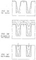
- Figures 1A-1C show steps in a conventional process.
- the starting structure will of course be defined by the previous process steps; but assume, for example, that the recesses have widths of 0.8 ⁇ m each, are spaced on a minimum pitch of 1.6 ⁇ m, and have a maximum depth of 1 ⁇ m. (Of course, these numbers are merely illustrative.)
- a first layer 1 of SOG would be spun on and cured, to a thickness of e.g. 300nm (3000 ⁇ ) in flat areas. (The thickness is substantially more in recessed areas.) As is well known to those of ordinary skill, the thickness of the SOG is determined by the individual composition and by the spin rate. As seen in Figure 1A, a single deposition of SOG is not enough to fill the recesses.
- a second layer 2 of SOG would then be spun on and cured, to provide an additional thickness of e.g. 300nm (3000 ⁇ ) in flat areas.
- a global etchback step is then performed, to remove the SOG from flat areas.
- the resulting surface contour as shown in Figure 1C, is susceptible to cracking.
- Figures 2A-2C show steps in a first embodiment of the invention. Assume that the same recess dimensions are used as in Figures 1A-1C. Again, the specific dimensions and parameters given here are merely illustrative, and do not delimit the invention.
- a first layer 1 of SOG is deposited as in Figure 1A. That is, for example, a siloxane-based spin-on glass (Such materials may be obtained, for example, from Ohka AmericaTM or Allied SignalTM or other suppliers.) is spun on to a thickness of 200nm (2000 ⁇ ) over flat areas, and is then cured for 60 minutes at 425°C.
- a siloxane-based spin-on glass (Such materials may be obtained, for example, from Ohka AmericaTM or Allied SignalTM or other suppliers.) is spun on to a thickness of 200nm (2000 ⁇ ) over flat areas, and is then cured for 60 minutes at 425°C.
- a layer 3 of low-temperature oxide is then deposited, to a thickness of 200nm (2000 ⁇ ). (For example, this may be done by plasma-enhanced deposition of TEOS.) This produces the structure shown in Figure 2B.
- a second layer 2 of SOG is then be spun on and cured, to provide an additional thickness of e.g. 300nm (3000 ⁇ ) in flat areas.
- a global etchback step is then performed, to remove the SOG and TEOS from flat areas.
- the resulting surface contour as shown in Figure 2C, provides improved filling of the recessed areas.
- the combination of slightly different materials reduces susceptibility to cracking.
- Figures 3A-3C show steps in a second embodiment of the invention. This may be particularly advantageous with more extreme topologies.
- the recessed areas have widths of 0.8 ⁇ m each, are spaced on a minimum pitch of 1.6 ⁇ m, and have a maximum depth of 2 ⁇ m. (Of course, these numbers are merely illustrative.)
- a first layer 1 of SOG is spun on and cured to produce a thickness of 200nm (2000 ⁇ ) over flat areas, as shown in Figure 3A.
- a layer 3 of low-temperature oxide is then deposited, to a thickness of 300nm (3000 ⁇ ). (For example, this may be done by plasma-enhanced deposition of TEOS.) This produces the structure shown in Figure 3B.
- a second layer 2 of SOG is then be spun on and cured, to provide an additional thickness of e.g. 200nm (2000 ⁇ ) in flat areas.
- a global etchback step is then performed, to remove the SOG and TEOS from flat areas.
- the resulting surface contour as shown in Figure 3C, provides improved filling of the recessed areas, even under extreme topologies.
- the combination of slightly different materials reduces susceptibility to cracking.
- a plasma oxide before the first layer of spin-on glass. (This is commonly done to prevent direct contact between the SOG and the underlying metallization.)
- 100nm-500nm (1000 ⁇ -5000 ⁇ ) of (for example) TEOS oxide would be deposited before the first layer of SOG.
- Processing then continues with deposition of an interlevel dielectric, such as PSG, and conventional further processing steps.
- an interlevel dielectric such as PSG
- One particular advantage of the disclosed invention is that it can be very easily implemented (in at least some processes) by a simple transposition of steps (depositing the low-temperature oxide before, rather than after, the second layer of spin-on glass).
- Figure 4 shows a sample device structure incorporating a planarization layer according to the disclosed innovations.
- the partially fabricated device structure included active devices 12 in a substrate 10, including polysilicon lines 14.
- Field oxide 13 provides lateral separation active devices.
- Metal lines 18 overlie a first interlevel dielectric 16 (e.g. of BPSG over TEOS), and make contact to active device areas at contact locations 20. (This provides the starting structure on which planarization is performed as described above.)
- a planarization layer 22 is then deposited, by the techniques described above, to reduce or eliminate the topographical excursions of the structure.
- An interlevel dielectric 24 overlies the planarization layer 22 (and the rest of the planarized structure), and includes via holes 25 through which a second metal layer 26 contacts the first metal layer 18.
- the structure shown can be topped by a protective overcoat (not shown) through which holes are etched to expose locations of contact pads in the second metal layer.
- the disclosed innovative steps have been described in the context of via formation (e.g. forming connections from second metal to first metal, or third metal to second metal). Due to the accumulated topographical excursions, planarization is especially desirable at these stages. However, the disclosed innovative concepts can also be applied to planarization of lower levels as well.
- the disclosed innovative concepts can also be applied to other spin-on materials, such as polyimide or polymethylmethacrylate.
Landscapes
- Internal Circuitry In Semiconductor Integrated Circuit Devices (AREA)
- Formation Of Insulating Films (AREA)
Claims (14)
- Verfahren zum Herstellen einer integrierten Schaltung, welches die Schritte aufweist:(a) Bereitstellen einer teilgefertigten integrierten Schaltungsstruktur mit leitenden Abschnitten an ihrer oberen Oberfläche, und mit einer unebenen Topographie mit hohen Stellen;(b) Aufbringen und Aushärten von ausgeschleudertem Glas, um eine erste dielektrische Schicht (1) auszubilden;(c) Abscheiden einer zweiten dielektrischen Schicht unter Vakuumbedingungen (3);(d) Aufbringen und Aushärten von ausgeschleudertem Glas, um eine dritte dielektrische Schicht (2) auszubilden;(e) Durchführen eines Gesamt-Rückätz-Schritts;(f) Abscheiden einer dielektrischen Zwischenschicht (24);(g) Ätzen von Löchern (25) an vorbestimmten Stellen in der dielektrischen Zwischenschicht; und(h) Abscheiden und Strukturieren einer Metallisierungsschicht (26), um eine gewünschte Struktur von Anschlüssen auszubilden, einschließlich elektrischer Anschlüsse durch die Löcher an die leitenden Abschnitte der integrierten Schaltung,
dadurch gekennzeichnet, daß vor dem Schritt (e) die dritte dielektrische Schicht (2) die zweite dielektrische Schicht (3) überdeckt, die die erste dielektrische Schicht (1) überdeckt, und daß der Gesamt-Rückätz-Schritt die dritte, zweite und erste dielektrische Schicht von den hohen Stellen der teilgefertigten Struktur entfernt, um eine geebnete Struktur auszubilden, die die teilgefertigte integrierte Schaltung und die verbleibenden Abschnitte der ersten, zweiten und dritten dielektrischen Schicht aufweist. - Verfahren gemäß Anspruch 1, bei welchem die zweite dielektrische Schicht (3) eine Siliziumdioxidschicht ist.
- Verfahren gemäß Anspruch 1 oder 2, bei welchem die zweite dielektrische Schicht (3) eine Dicke hat, die kleiner oder gleich derjenigen der ersten dielektrischen Schicht (1) ist, und die dritte dielektrische Schicht (2) eine Dicke hat, die größer oder gleich derjenigen der zweiten dielektrischen Schicht (3) ist.
- Verfahren gemäß einem der Ansprüche 1 bis 3, bei welchem der Abscheidschritt (c) plasmaverstärkt ist.
- Verfahren gemäß einem der Ansprüche 1 bis 3, bei welchem beim Abscheidschritt (c) Tetraethoxysilan als Quellgas verwendet wird.
- Verfahren gemäß einem der Ansprüche 1 bis 3, welches den zusätzlichen Schritt aufweist: Aufbringen eines passivierenden Dielektrikums unter Vakuumbedingungen nach dem Schritt (a) und vor dem Abscheidschritt (b).
- Verfahren gemäß einem der Ansprüche 1 bis 3, bei welchem beim Abscheidschritt (b) das ausgeschleuderte Glas mit einer Dicke im Bereich einschließlich 100-500 nm aufgebracht wird.
- Verfahren gemäß einem der Ansprüche 1 bis 3, bei welchem die dielektrische Zwischenschicht (24) ein dotiertes Silikatglas ist.
- Verfahren gemäß einem der Ansprüche 1 bis 3, bei welchem beim Abscheidschritt (d) das ausgeschleuderte Glas mit einer Dicke im Bereich einschließlich 100-500 nm aufgebracht wird.
- Verfahren gemäß einem der vorhergehenden Ansprüche, bei welchem die zweite dielektrische Schicht (3) dotiert ist.
- Verfahren gemäß einem der vorhergehenden Ansprüche, bei welchem die zweite dielektrische Schicht (3) ein Niedertemperaturoxid ist.
- Verfahren gemäß einem der vorhergehenden Ansprüche, bei welchem die zweite dielektrische Schicht (3) aus der Gasphase abgeschieden wird.
- Integrierte Schaltung, welche aufweist:eine unten liegende Struktur, welche ein Substrat enthält, aktive Bauelementstrukturen, Isolierstrukturen, und eine oder mehrere strukturierte Dünnfilmleitschichten mit einer oberen Leitschicht, wobei die unten liegende Struktur eine unebene Topographie mit Vertiefungen und hohen Stellen aufweist;eine Planarisierungsstruktur in den Vertiefungen der unten liegenden Struktur, welche ausgeschleudertes Glas aufweist;eine dielektrische Zwischenschicht (24), welche die Planarisierungsstruktur und die unten liegende Struktur überdeckt, und Löcher (25) aufweist; undeine dünnfilmstrukturierte Leitschicht, welche die dielektrische Zwischenschicht überdeckt, und sich durch die Löcher zu ausgewählten Stellen der oberen Leitschicht erstreckt, dadurch gekennzeichnet, daß die Planarisierungsstruktur in den Vertiefungen der unten liegenden Struktur ein erstes Dielektrikum (1) aufweist, über welchem ein zweites Dielektrikum (3) liegt, über welchem ein drittes Dielektrikum (2) liegt, wobei das erste und dritte Dielektrikum ausgeschleudertes Glas sind, und die Planarisierungsstruktur die hohen Punkte nicht überdeckt.
- Integrierte Schaltung gemäß Anspruch 13, bei welcher das zweite Dielektrikum (3) Siliziumdioxid ist.
Applications Claiming Priority (2)
| Application Number | Priority Date | Filing Date | Title |
|---|---|---|---|
| US163043 | 1993-12-06 | ||
| US08/163,043 US5435888A (en) | 1993-12-06 | 1993-12-06 | Enhanced planarization technique for an integrated circuit |
Publications (2)
| Publication Number | Publication Date |
|---|---|
| EP0657925A1 EP0657925A1 (de) | 1995-06-14 |
| EP0657925B1 true EP0657925B1 (de) | 2000-08-23 |
Family
ID=22588229
Family Applications (1)
| Application Number | Title | Priority Date | Filing Date |
|---|---|---|---|
| EP94308498A Expired - Lifetime EP0657925B1 (de) | 1993-12-06 | 1994-11-17 | Planarisierungstechnik für eine integrierte Schaltung |
Country Status (4)
| Country | Link |
|---|---|
| US (5) | US5435888A (de) |
| EP (1) | EP0657925B1 (de) |
| JP (1) | JPH07201997A (de) |
| DE (1) | DE69425636T2 (de) |
Families Citing this family (65)
| Publication number | Priority date | Publication date | Assignee | Title |
|---|---|---|---|---|
| US5435888A (en) * | 1993-12-06 | 1995-07-25 | Sgs-Thomson Microelectronics, Inc. | Enhanced planarization technique for an integrated circuit |
| DE4432294A1 (de) * | 1994-09-12 | 1996-03-14 | Telefunken Microelectron | Verfahren zur Reduzierung der Oberflächenrekombinationsgeschwindigkeit in Silizium |
| US5534731A (en) * | 1994-10-28 | 1996-07-09 | Advanced Micro Devices, Incorporated | Layered low dielectric constant technology |
| JP3369817B2 (ja) * | 1995-06-23 | 2003-01-20 | 三菱電機株式会社 | 半導体装置 |
| US5631197A (en) * | 1995-08-30 | 1997-05-20 | Taiwan Semiconductor Manufacturing Company, Ltd | Sacrificial etchback layer for improved spin-on-glass planarization |
| US5770469A (en) * | 1995-12-29 | 1998-06-23 | Lam Research Corporation | Method for forming semiconductor structure using modulation doped silicate glasses |
| US5691247A (en) * | 1996-12-19 | 1997-11-25 | Tower Semiconductor Ltd. | Method for depositing a flow fill layer on an integrated circuit wafer |
| US5850105A (en) | 1997-03-21 | 1998-12-15 | Advanced Micro Devices, Inc. | Substantially planar semiconductor topography using dielectrics and chemical mechanical polish |
| JP3909912B2 (ja) * | 1997-05-09 | 2007-04-25 | 東京応化工業株式会社 | シリカ系厚膜被膜形成方法 |
| US5814564A (en) * | 1997-05-15 | 1998-09-29 | Vanguard International Semiconductor Corporation | Etch back method to planarize an interlayer having a critical HDP-CVD deposition process |
| JP2000031488A (ja) * | 1997-08-26 | 2000-01-28 | Semiconductor Energy Lab Co Ltd | 半導体装置およびその作製方法 |
| GB9718931D0 (en) * | 1997-09-05 | 1997-11-12 | Imperial College | Sol gel process |
| US6114219A (en) * | 1997-09-15 | 2000-09-05 | Advanced Micro Devices, Inc. | Method of manufacturing an isolation region in a semiconductor device using a flowable oxide-generating material |
| US5918152A (en) * | 1997-09-19 | 1999-06-29 | Chartered Semiconductor Manufacturing, Ltd. | Gap filling method using high pressure |
| US6054390A (en) * | 1997-11-05 | 2000-04-25 | Chartered Semiconductor Manufacturing Ltd. | Grazing incident angle processing method for microelectronics layer fabrication |
| US5933747A (en) * | 1997-12-18 | 1999-08-03 | Advanced Micro Devices, Inc. | Method and structure for an advanced isolation spacer shell |
| US6376359B1 (en) * | 1998-03-18 | 2002-04-23 | United Microelectronics Corp. | Method of manufacturing metallic interconnect |
| US6017780A (en) * | 1998-07-06 | 2000-01-25 | Chartered Semiconductor Manufacturing, Ltd. | Passivation scheme for LCD and other applications |
| US6114220A (en) * | 1998-11-18 | 2000-09-05 | United Microelectronics Corp. | Method of fabricating a shallow trench isolation |
| US6008108A (en) * | 1998-12-07 | 1999-12-28 | United Microelectronics Corp. | Method of fabricating a shallow-trench isolation structure in an integrated circuit |
| US6204149B1 (en) * | 1999-05-26 | 2001-03-20 | Micron Technology, Inc. | Methods of forming polished material and methods of forming isolation regions |
| US6303043B1 (en) * | 1999-07-07 | 2001-10-16 | United Microelectronics Corp. | Method of fabricating preserve layer |
| US6465325B2 (en) * | 2001-02-27 | 2002-10-15 | Fairchild Semiconductor Corporation | Process for depositing and planarizing BPSG for dense trench MOSFET application |
| KR100512167B1 (ko) * | 2001-03-12 | 2005-09-02 | 삼성전자주식회사 | 트렌치 소자 분리형 반도체 장치 및 트렌치형 소자 분리막형성방법 |
| KR100428805B1 (ko) * | 2001-08-09 | 2004-04-28 | 삼성전자주식회사 | 트렌치 소자분리 구조체 및 그 형성 방법 |
| US6503848B1 (en) | 2001-11-20 | 2003-01-07 | Taiwan Semiconductor Manufacturing Company | Method of forming a smooth polysilicon surface using a soft etch to enlarge the photo lithography window |
| JP2004022575A (ja) * | 2002-06-12 | 2004-01-22 | Sanyo Electric Co Ltd | 半導体装置 |
| US7323417B2 (en) * | 2004-09-21 | 2008-01-29 | Molecular Imprints, Inc. | Method of forming a recessed structure employing a reverse tone process |
| KR20070029655A (ko) * | 2003-12-19 | 2007-03-14 | 써드 디멘존 세미컨덕터, 인코포레이티드 | 넓은 메사를 갖는 수퍼 접합 장치의 제조 방법 |
| EP1701686A4 (de) * | 2003-12-19 | 2009-07-01 | Third Dimension 3D Sc Inc | Verfahren zur herstellung einer superverbindungsvorrichtung mit herkömmlichen enden |
| US7023069B2 (en) * | 2003-12-19 | 2006-04-04 | Third Dimension (3D) Semiconductor, Inc. | Method for forming thick dielectric regions using etched trenches |
| JP4928947B2 (ja) | 2003-12-19 | 2012-05-09 | サード ディメンジョン (スリーディ) セミコンダクタ インコーポレイテッド | 超接合デバイスの製造方法 |
| WO2005065144A2 (en) * | 2003-12-19 | 2005-07-21 | Third Dimension (3D) Semiconductor, Inc. | Planarization method of manufacturing a superjunction device |
| US8989523B2 (en) | 2004-01-22 | 2015-03-24 | Vescent Photonics, Inc. | Liquid crystal waveguide for dynamically controlling polarized light |
| US7720116B2 (en) * | 2004-01-22 | 2010-05-18 | Vescent Photonics, Inc. | Tunable laser having liquid crystal waveguide |
| US20050271325A1 (en) * | 2004-01-22 | 2005-12-08 | Anderson Michael H | Liquid crystal waveguide having refractive shapes for dynamically controlling light |
| US8860897B1 (en) | 2004-01-22 | 2014-10-14 | Vescent Photonics, Inc. | Liquid crystal waveguide having electric field orientated for controlling light |
| US8463080B1 (en) | 2004-01-22 | 2013-06-11 | Vescent Photonics, Inc. | Liquid crystal waveguide having two or more control voltages for controlling polarized light |
| US7205244B2 (en) | 2004-09-21 | 2007-04-17 | Molecular Imprints | Patterning substrates employing multi-film layers defining etch-differential interfaces |
| US7547504B2 (en) | 2004-09-21 | 2009-06-16 | Molecular Imprints, Inc. | Pattern reversal employing thick residual layers |
| US7439583B2 (en) * | 2004-12-27 | 2008-10-21 | Third Dimension (3D) Semiconductor, Inc. | Tungsten plug drain extension |
| TWI401749B (zh) * | 2004-12-27 | 2013-07-11 | 3D半導體股份有限公司 | 用於高電壓超接面終止之方法 |
| JP2008538659A (ja) * | 2005-04-22 | 2008-10-30 | アイスモス テクノロジー コーポレイション | 酸化物で内面が覆われた溝を有する超接合素子と酸化物で内面を覆われた溝を有する超接合素子を製造するための方法 |
| US7446018B2 (en) * | 2005-08-22 | 2008-11-04 | Icemos Technology Corporation | Bonded-wafer superjunction semiconductor device |
| US7570320B1 (en) | 2005-09-01 | 2009-08-04 | Vescent Photonics, Inc. | Thermo-optic liquid crystal waveguides |
| KR100746223B1 (ko) * | 2005-09-09 | 2007-08-03 | 삼성전자주식회사 | 반도체소자의 트렌치 소자분리 방법 |
| US20070077763A1 (en) * | 2005-09-30 | 2007-04-05 | Molecular Imprints, Inc. | Deposition technique to planarize a multi-layer structure |
| KR101026479B1 (ko) * | 2006-12-28 | 2011-04-01 | 주식회사 하이닉스반도체 | 반도체 소자 및 그의 제조 방법 |
| US7723172B2 (en) * | 2007-04-23 | 2010-05-25 | Icemos Technology Ltd. | Methods for manufacturing a trench type semiconductor device having a thermally sensitive refill material |
| US8580651B2 (en) * | 2007-04-23 | 2013-11-12 | Icemos Technology Ltd. | Methods for manufacturing a trench type semiconductor device having a thermally sensitive refill material |
| US20080272429A1 (en) * | 2007-05-04 | 2008-11-06 | Icemos Technology Corporation | Superjunction devices having narrow surface layout of terminal structures and methods of manufacturing the devices |
| US20090085148A1 (en) * | 2007-09-28 | 2009-04-02 | Icemos Technology Corporation | Multi-directional trenching of a plurality of dies in manufacturing superjunction devices |
| KR100891533B1 (ko) * | 2007-10-26 | 2009-04-03 | 주식회사 하이닉스반도체 | 반도체 소자의 소자분리막 형성방법 |
| KR100891535B1 (ko) * | 2007-10-26 | 2009-04-03 | 주식회사 하이닉스반도체 | 반도체 소자의 소자분리막 형성방법 |
| US7846821B2 (en) * | 2008-02-13 | 2010-12-07 | Icemos Technology Ltd. | Multi-angle rotation for ion implantation of trenches in superjunction devices |
| US8030133B2 (en) * | 2008-03-28 | 2011-10-04 | Icemos Technology Ltd. | Method of fabricating a bonded wafer substrate for use in MEMS structures |
| KR101003496B1 (ko) * | 2008-09-29 | 2010-12-30 | 주식회사 하이닉스반도체 | 소자분리 구조 및 리세스 게이트를 포함하는 반도체 소자 및 제조 방법 |
| US9366938B1 (en) | 2009-02-17 | 2016-06-14 | Vescent Photonics, Inc. | Electro-optic beam deflector device |
| US8995038B1 (en) | 2010-07-06 | 2015-03-31 | Vescent Photonics, Inc. | Optical time delay control device |
| US8946814B2 (en) | 2012-04-05 | 2015-02-03 | Icemos Technology Ltd. | Superjunction devices having narrow surface layout of terminal structures, buried contact regions and trench gates |
| US9252080B1 (en) * | 2014-10-15 | 2016-02-02 | Globalfoundries Inc. | Dielectric cover for a through silicon via |
| TWI687987B (zh) * | 2015-02-17 | 2020-03-11 | 愛爾蘭商滿捷特科技公司 | 填充蝕刻洞的製程 |
| KR101926294B1 (ko) | 2015-03-30 | 2018-12-06 | 미쓰이 가가쿠 가부시키가이샤 | 매입 평탄화막의 제조 방법 및 전자 디바이스의 제조 방법 |
| US9799529B2 (en) * | 2016-03-17 | 2017-10-24 | Taiwan Semiconductor Manufacturing Co., Ltd. | Method of planarizing a film layer |
| US11201122B2 (en) | 2018-09-27 | 2021-12-14 | Taiwan Semiconductor Manufacturing Co., Ltd. | Method of fabricating semiconductor device with reduced warpage and better trench filling performance |
Family Cites Families (65)
| Publication number | Priority date | Publication date | Assignee | Title |
|---|---|---|---|---|
| DE410244C (de) | 1924-02-02 | 1925-02-26 | Friedrich Lunow | Loseblaetterbuch mit schwingbar gelagerten ineinander eintretenden Aufreihern |
| US4253907A (en) * | 1979-03-28 | 1981-03-03 | Western Electric Company, Inc. | Anisotropic plasma etching |
| US4354896A (en) * | 1980-08-05 | 1982-10-19 | Texas Instruments Incorporated | Formation of submicron substrate element |
| US4333964A (en) * | 1980-09-15 | 1982-06-08 | General Electric Company | Method of making integrated circuits |
| JPS5871589A (ja) * | 1981-10-22 | 1983-04-28 | シャープ株式会社 | 薄膜el素子 |
| US4384938A (en) * | 1982-05-03 | 1983-05-24 | International Business Machines Corporation | Reactive ion etching chamber |
| JPS59106172A (ja) * | 1982-12-07 | 1984-06-19 | インタ−ナシヨナル ビジネス マシ−ンズ コ−ポレ−シヨン | 電界効果トランジスタの製造方法 |
| JPS6058635A (ja) * | 1983-09-12 | 1985-04-04 | Toshiba Corp | 半導体装置の製造方法 |
| JPS6126240A (ja) * | 1984-07-17 | 1986-02-05 | Hitachi Ltd | 絶縁分離方法 |
| US4654112A (en) * | 1984-09-26 | 1987-03-31 | Texas Instruments Incorporated | Oxide etch |
| EP0185787B1 (de) * | 1984-12-21 | 1988-08-10 | Deutsche ITT Industries GmbH | Plastikumhülltes Halbleiterbauelement |
| US4686000A (en) * | 1985-04-02 | 1987-08-11 | Heath Barbara A | Self-aligned contact process |
| JPS61232646A (ja) * | 1985-04-09 | 1986-10-16 | Nec Corp | 樹脂封止型半導体集積回路装置 |
| US4657628A (en) * | 1985-05-01 | 1987-04-14 | Texas Instruments Incorporated | Process for patterning local interconnects |
| JPS61292951A (ja) * | 1985-06-21 | 1986-12-23 | Hitachi Ltd | 半導体集積回路装置の製法 |
| US4660278A (en) * | 1985-06-26 | 1987-04-28 | Texas Instruments Incorporated | Process of making IC isolation structure |
| JPH0789562B2 (ja) * | 1985-11-01 | 1995-09-27 | 富士通株式会社 | 集積回路の素子分離方法 |
| US4755476A (en) * | 1985-12-17 | 1988-07-05 | Siemens Aktiengesellschaft | Process for the production of self-adjusted bipolar transistor structures having a reduced extrinsic base resistance |
| JPS62150826A (ja) * | 1985-12-25 | 1987-07-04 | Toshiba Corp | 半導体装置の製造方法 |
| EP0232508B1 (de) * | 1986-01-09 | 1992-03-11 | International Business Machines Corporation | Verfahren zur Herstellung eines Kontakts unter Verwendung der Erweichung zweier Glasschichten |
| JP2523488B2 (ja) * | 1986-04-18 | 1996-08-07 | 株式会社日立製作所 | 半導体記憶装置 |
| US4676867A (en) * | 1986-06-06 | 1987-06-30 | Rockwell International Corporation | Planarization process for double metal MOS using spin-on glass as a sacrificial layer |
| US4707218A (en) * | 1986-10-28 | 1987-11-17 | International Business Machines Corporation | Lithographic image size reduction |
| US4872947A (en) * | 1986-12-19 | 1989-10-10 | Applied Materials, Inc. | CVD of silicon oxide using TEOS decomposition and in-situ planarization process |
| US4801350A (en) * | 1986-12-29 | 1989-01-31 | Motorola, Inc. | Method for obtaining submicron features from optical lithography technology |
| US4721548A (en) * | 1987-05-13 | 1988-01-26 | Intel Corporation | Semiconductor planarization process |
| JPS63293946A (ja) * | 1987-05-27 | 1988-11-30 | Matsushita Electric Ind Co Ltd | 半導体装置の製造方法 |
| GB2207281B (en) * | 1987-07-24 | 1992-02-05 | Plessey Co Plc | A method of providing refilled trenches |
| US4801560A (en) * | 1987-10-02 | 1989-01-31 | Motorola Inc. | Semiconductor processing utilizing carbon containing thick film spin-on glass |
| FR2625839B1 (fr) * | 1988-01-13 | 1991-04-26 | Sgs Thomson Microelectronics | Procede de passivation d'un circuit integre |
| US4962414A (en) * | 1988-02-11 | 1990-10-09 | Sgs-Thomson Microelectronics, Inc. | Method for forming a contact VIA |
| US4894351A (en) * | 1988-02-16 | 1990-01-16 | Sprague Electric Company | Method for making a silicon IC with planar double layer metal conductors system |
| US4912061A (en) * | 1988-04-04 | 1990-03-27 | Digital Equipment Corporation | Method of forming a salicided self-aligned metal oxide semiconductor device using a disposable silicon nitride spacer |
| JPH0770623B2 (ja) * | 1988-07-08 | 1995-07-31 | 三菱電機株式会社 | スタティックランダムアクセスメモリ装置 |
| US4986878A (en) * | 1988-07-19 | 1991-01-22 | Cypress Semiconductor Corp. | Process for improved planarization of the passivation layers for semiconductor devices |
| JP2805765B2 (ja) * | 1988-09-13 | 1998-09-30 | ソニー株式会社 | 半導体メモリ装置 |
| US5244841A (en) * | 1988-11-10 | 1993-09-14 | Applied Materials, Inc. | Method for planarizing an integrated circuit structure using low melting inorganic material and flowing while depositing |
| US5204288A (en) * | 1988-11-10 | 1993-04-20 | Applied Materials, Inc. | Method for planarizing an integrated circuit structure using low melting inorganic material |
| GB8901236D0 (en) * | 1989-01-20 | 1989-03-15 | Ensor Charles H | Improved display device |
| US5068711A (en) * | 1989-03-20 | 1991-11-26 | Fujitsu Limited | Semiconductor device having a planarized surface |
| KR920004541B1 (ko) * | 1989-05-30 | 1992-06-08 | 현대전자산업 주식회사 | 반도체 소자에서 식각베리어층을 사용한 콘택홀 형성방법 |
| US5083190A (en) * | 1989-09-05 | 1992-01-21 | Motorola, Inc. | Shared gate CMOS transistor |
| JPH03133131A (ja) * | 1989-10-18 | 1991-06-06 | Mitsubishi Electric Corp | 半導体装置 |
| JP2518435B2 (ja) * | 1990-01-29 | 1996-07-24 | ヤマハ株式会社 | 多層配線形成法 |
| CA2009518C (en) * | 1990-02-07 | 2000-10-17 | Luc Ouellet | Spin-on glass processing technique for the fabrication of semiconductor device |
| US5003062A (en) * | 1990-04-19 | 1991-03-26 | Taiwan Semiconductor Manufacturing Co. | Semiconductor planarization process for submicron devices |
| DE69121629T2 (de) * | 1990-04-27 | 1997-02-13 | Nippon Electric Co | Dünnfilmtransistor mit Schottky-Sperrschicht |
| US5166088A (en) * | 1990-07-03 | 1992-11-24 | Sharp Kabushiki Kaisha | Method of manufacturing semiconductor device contact vias in layers comprising silicon nitride and glass |
| EP0469214A1 (de) * | 1990-07-31 | 1992-02-05 | International Business Machines Corporation | Verfahren zur Herstellung geschichteter Leiter- und/oder Widerstandsbereiche in Multiebenen-Halbleiterbauelementen und daraus resultierende Struktur |
| JP3128811B2 (ja) * | 1990-08-07 | 2001-01-29 | セイコーエプソン株式会社 | 半導体装置の製造方法 |
| JPH0492453A (ja) * | 1990-08-08 | 1992-03-25 | Seiko Epson Corp | 半導体装置 |
| US5158910A (en) * | 1990-08-13 | 1992-10-27 | Motorola Inc. | Process for forming a contact structure |
| US5117273A (en) * | 1990-11-16 | 1992-05-26 | Sgs-Thomson Microelectronics, Inc. | Contact for integrated circuits |
| IT1243919B (it) * | 1990-11-20 | 1994-06-28 | Cons Ric Microelettronica | Procedimento per l'ottenimento di solchi submicrometrici planarizzati in circuiti integrati realizzati con tecnologia ulsi |
| US5290399A (en) * | 1991-02-05 | 1994-03-01 | Advanced Micro Devices, Inc. | Surface planarizing methods for integrated circuit devices |
| JPH0574958A (ja) * | 1991-09-13 | 1993-03-26 | Nec Corp | 半導体装置およびその製造方法 |
| US5266516A (en) * | 1992-01-02 | 1993-11-30 | Chartered Semiconductor Manufacturing Pte Ltd | Method for making electrical contact through an opening of one micron or less for CMOS technology |
| JPH05243223A (ja) * | 1992-02-28 | 1993-09-21 | Fujitsu Ltd | 集積回路装置の製造方法 |
| EP0582724A1 (de) * | 1992-08-04 | 1994-02-16 | Siemens Aktiengesellschaft | Verfahren zur lokal und global planarisierenden CVD-Abscheidung von SiO2-Schichten auf strukturierten Siliziumsubstraten |
| US5250472A (en) * | 1992-09-03 | 1993-10-05 | Industrial Technology Research Institute | Spin-on-glass integration planarization having siloxane partial etchback and silicate processes |
| US5331117A (en) * | 1992-11-12 | 1994-07-19 | Sgs-Thomson Microelectronics, Inc. | Method to improve interlevel dielectric planarization |
| US5373170A (en) * | 1993-03-15 | 1994-12-13 | Motorola Inc. | Semiconductor memory device having a compact symmetrical layout |
| US5399533A (en) * | 1993-12-01 | 1995-03-21 | Vlsi Technology, Inc. | Method improving integrated circuit planarization during etchback |
| US5435888A (en) * | 1993-12-06 | 1995-07-25 | Sgs-Thomson Microelectronics, Inc. | Enhanced planarization technique for an integrated circuit |
| US5534731A (en) * | 1994-10-28 | 1996-07-09 | Advanced Micro Devices, Incorporated | Layered low dielectric constant technology |
-
1993
- 1993-12-06 US US08/163,043 patent/US5435888A/en not_active Expired - Lifetime
-
1994
- 1994-11-17 DE DE69425636T patent/DE69425636T2/de not_active Expired - Fee Related
- 1994-11-17 EP EP94308498A patent/EP0657925B1/de not_active Expired - Lifetime
- 1994-12-06 JP JP6301868A patent/JPH07201997A/ja active Pending
-
1996
- 1996-07-15 US US08/679,946 patent/US5633534A/en not_active Expired - Lifetime
-
1997
- 1997-11-24 US US08/976,760 patent/US5837613A/en not_active Expired - Lifetime
-
1998
- 1998-01-15 US US09/007,668 patent/US5986330A/en not_active Ceased
-
2001
- 2001-11-16 US US09/998,595 patent/USRE39690E1/en not_active Expired - Lifetime
Also Published As
| Publication number | Publication date |
|---|---|
| US5435888A (en) | 1995-07-25 |
| JPH07201997A (ja) | 1995-08-04 |
| DE69425636D1 (de) | 2000-09-28 |
| DE69425636T2 (de) | 2001-01-25 |
| EP0657925A1 (de) | 1995-06-14 |
| US5633534A (en) | 1997-05-27 |
| US5837613A (en) | 1998-11-17 |
| US5986330A (en) | 1999-11-16 |
| USRE39690E1 (en) | 2007-06-12 |
Similar Documents
| Publication | Publication Date | Title |
|---|---|---|
| EP0657925B1 (de) | Planarisierungstechnik für eine integrierte Schaltung | |
| US5393708A (en) | Inter-metal-dielectric planarization process | |
| KR900004264B1 (ko) | 스핀-온 그라스를 쎄크리휘셜층으로 사용하는 2중금속층 mos의 평탄화 방법 | |
| KR0160338B1 (ko) | 반도체 장치의 제조 방법 | |
| US5607773A (en) | Method of forming a multilevel dielectric | |
| US5003062A (en) | Semiconductor planarization process for submicron devices | |
| US5250472A (en) | Spin-on-glass integration planarization having siloxane partial etchback and silicate processes | |
| US7602048B2 (en) | Semiconductor device and semiconductor wafer having a multi-layered insulation film | |
| KR100373804B1 (ko) | 서브미크론상호연결의선택적간극충진을위한2단계마스킹방법 | |
| US6114186A (en) | Hydrogen silsesquioxane thin films for low capacitance structures in integrated circuits | |
| US5665657A (en) | Spin-on-glass partial etchback planarization process | |
| KR20010031049A (ko) | 하이드로겐-실세스퀴옥산(hsq)으로 갭이 채워진패터닝된 금속층을 사용한 경계 없는 비아들 | |
| KR100382376B1 (ko) | 반도체 장치 및 그의 제조방법 | |
| US6207554B1 (en) | Gap filling process in integrated circuits using low dielectric constant materials | |
| US5804503A (en) | Method and structure for reducing microelectronic short circuits using spin-on glass as part of the interlayer dielectric | |
| KR20050013492A (ko) | 구리/낮은 k 상호 접속 구조를 위해 개선된 화학적평탄화 성능 | |
| US5366850A (en) | Submicron planarization process with passivation on metal line | |
| US5567660A (en) | Spin-on-glass planarization by a new stagnant coating method | |
| US6093635A (en) | High integrity borderless vias with HSQ gap filled patterned conductive layers | |
| US5930677A (en) | Method for reducing microloading in an etchback of spin-on-glass or polymer | |
| US6030891A (en) | Vacuum baked HSQ gap fill layer for high integrity borderless vias | |
| US5817571A (en) | Multilayer interlevel dielectrics using phosphorus-doped glass | |
| US5597764A (en) | Method of contact formation and planarization for semiconductor processes | |
| WO1991010261A1 (en) | Semiconductor interconnect structure utilizing a polyimide insulator | |
| US6784095B1 (en) | Phosphine treatment of low dielectric constant materials in semiconductor device manufacturing |
Legal Events
| Date | Code | Title | Description |
|---|---|---|---|
| PUAI | Public reference made under article 153(3) epc to a published international application that has entered the european phase |
Free format text: ORIGINAL CODE: 0009012 |
|
| AK | Designated contracting states |
Kind code of ref document: A1 Designated state(s): DE FR GB IT |
|
| 17P | Request for examination filed |
Effective date: 19951214 |
|
| 17Q | First examination report despatched |
Effective date: 19961218 |
|
| RAP3 | Party data changed (applicant data changed or rights of an application transferred) |
Owner name: STMICROELECTRONICS, INC. |
|
| RTI1 | Title (correction) |
Free format text: PLANARIZATION TECHNIQUE FOR AN INTEGRATED CIRCUIT |
|
| GRAG | Despatch of communication of intention to grant |
Free format text: ORIGINAL CODE: EPIDOS AGRA |
|
| GRAG | Despatch of communication of intention to grant |
Free format text: ORIGINAL CODE: EPIDOS AGRA |
|
| GRAH | Despatch of communication of intention to grant a patent |
Free format text: ORIGINAL CODE: EPIDOS IGRA |
|
| GRAH | Despatch of communication of intention to grant a patent |
Free format text: ORIGINAL CODE: EPIDOS IGRA |
|
| GRAA | (expected) grant |
Free format text: ORIGINAL CODE: 0009210 |
|
| AK | Designated contracting states |
Kind code of ref document: B1 Designated state(s): DE FR GB IT |
|
| REF | Corresponds to: |
Ref document number: 69425636 Country of ref document: DE Date of ref document: 20000928 |
|
| ITF | It: translation for a ep patent filed | ||
| ET | Fr: translation filed | ||
| PLBE | No opposition filed within time limit |
Free format text: ORIGINAL CODE: 0009261 |
|
| STAA | Information on the status of an ep patent application or granted ep patent |
Free format text: STATUS: NO OPPOSITION FILED WITHIN TIME LIMIT |
|
| 26N | No opposition filed | ||
| REG | Reference to a national code |
Ref country code: GB Ref legal event code: IF02 |
|
| PGFP | Annual fee paid to national office [announced via postgrant information from national office to epo] |
Ref country code: DE Payment date: 20041111 Year of fee payment: 11 |
|
| PG25 | Lapsed in a contracting state [announced via postgrant information from national office to epo] |
Ref country code: IT Free format text: LAPSE BECAUSE OF NON-PAYMENT OF DUE FEES Effective date: 20051117 |
|
| PG25 | Lapsed in a contracting state [announced via postgrant information from national office to epo] |
Ref country code: DE Free format text: LAPSE BECAUSE OF NON-PAYMENT OF DUE FEES Effective date: 20060601 |
|
| PGFP | Annual fee paid to national office [announced via postgrant information from national office to epo] |
Ref country code: GB Payment date: 20131025 Year of fee payment: 20 Ref country code: FR Payment date: 20131121 Year of fee payment: 20 |
|
| REG | Reference to a national code |
Ref country code: GB Ref legal event code: PE20 Expiry date: 20141116 |
|
| PG25 | Lapsed in a contracting state [announced via postgrant information from national office to epo] |
Ref country code: GB Free format text: LAPSE BECAUSE OF EXPIRATION OF PROTECTION Effective date: 20141116 |