EP0657977A2 - Laser mit Streifenstruktur und Herstellungsverfahren - Google Patents
Laser mit Streifenstruktur und Herstellungsverfahren Download PDFInfo
- Publication number
- EP0657977A2 EP0657977A2 EP94119425A EP94119425A EP0657977A2 EP 0657977 A2 EP0657977 A2 EP 0657977A2 EP 94119425 A EP94119425 A EP 94119425A EP 94119425 A EP94119425 A EP 94119425A EP 0657977 A2 EP0657977 A2 EP 0657977A2
- Authority
- EP
- European Patent Office
- Prior art keywords
- layer
- current blocking
- blocking layer
- laser diode
- semiconductor laser
- Prior art date
- Legal status (The legal status is an assumption and is not a legal conclusion. Google has not performed a legal analysis and makes no representation as to the accuracy of the status listed.)
- Granted
Links
- 238000000034 method Methods 0.000 title claims abstract description 39
- 230000000903 blocking effect Effects 0.000 claims abstract description 63
- 238000005253 cladding Methods 0.000 claims abstract description 39
- 239000004065 semiconductor Substances 0.000 claims abstract description 38
- 239000000463 material Substances 0.000 claims abstract description 23
- 239000000758 substrate Substances 0.000 claims abstract description 14
- 238000000927 vapour-phase epitaxy Methods 0.000 claims abstract description 5
- 238000005530 etching Methods 0.000 claims description 7
- 229910000530 Gallium indium arsenide Inorganic materials 0.000 claims description 3
- 238000001704 evaporation Methods 0.000 abstract description 4
- 238000004519 manufacturing process Methods 0.000 abstract description 4
- VEXZGXHMUGYJMC-UHFFFAOYSA-N Hydrochloric acid Chemical compound Cl VEXZGXHMUGYJMC-UHFFFAOYSA-N 0.000 description 18
- 229910000041 hydrogen chloride Inorganic materials 0.000 description 17
- IXCSERBJSXMMFS-UHFFFAOYSA-N hydrogen chloride Substances Cl.Cl IXCSERBJSXMMFS-UHFFFAOYSA-N 0.000 description 17
- 239000007789 gas Substances 0.000 description 16
- 229910001218 Gallium arsenide Inorganic materials 0.000 description 14
- 238000010586 diagram Methods 0.000 description 6
- 238000009792 diffusion process Methods 0.000 description 5
- 229910000980 Aluminium gallium arsenide Inorganic materials 0.000 description 4
- 229910052782 aluminium Inorganic materials 0.000 description 4
- 239000013078 crystal Substances 0.000 description 3
- 230000006866 deterioration Effects 0.000 description 3
- 238000002149 energy-dispersive X-ray emission spectroscopy Methods 0.000 description 3
- 230000003287 optical effect Effects 0.000 description 3
- QAOWNCQODCNURD-UHFFFAOYSA-N Sulfuric acid Chemical compound OS(O)(=O)=O QAOWNCQODCNURD-UHFFFAOYSA-N 0.000 description 2
- 238000010521 absorption reaction Methods 0.000 description 2
- 230000015572 biosynthetic process Effects 0.000 description 2
- 230000000694 effects Effects 0.000 description 2
- 230000002708 enhancing effect Effects 0.000 description 2
- 238000012360 testing method Methods 0.000 description 2
- 229910052581 Si3N4 Inorganic materials 0.000 description 1
- 229910004205 SiNX Inorganic materials 0.000 description 1
- 230000002411 adverse Effects 0.000 description 1
- XAGFODPZIPBFFR-UHFFFAOYSA-N aluminium Chemical compound [Al] XAGFODPZIPBFFR-UHFFFAOYSA-N 0.000 description 1
- 238000007796 conventional method Methods 0.000 description 1
- 238000005259 measurement Methods 0.000 description 1
- 230000010355 oscillation Effects 0.000 description 1
- 238000000206 photolithography Methods 0.000 description 1
- 238000000623 plasma-assisted chemical vapour deposition Methods 0.000 description 1
- 238000011160 research Methods 0.000 description 1
- HQVNEWCFYHHQES-UHFFFAOYSA-N silicon nitride Chemical compound N12[Si]34N5[Si]62N3[Si]51N64 HQVNEWCFYHHQES-UHFFFAOYSA-N 0.000 description 1
- 230000001629 suppression Effects 0.000 description 1
- 238000001039 wet etching Methods 0.000 description 1
Images

Classifications
-
- B—PERFORMING OPERATIONS; TRANSPORTING
- B82—NANOTECHNOLOGY
- B82Y—SPECIFIC USES OR APPLICATIONS OF NANOSTRUCTURES; MEASUREMENT OR ANALYSIS OF NANOSTRUCTURES; MANUFACTURE OR TREATMENT OF NANOSTRUCTURES
- B82Y20/00—Nanooptics, e.g. quantum optics or photonic crystals
-
- H—ELECTRICITY
- H01—ELECTRIC ELEMENTS
- H01S—DEVICES USING THE PROCESS OF LIGHT AMPLIFICATION BY STIMULATED EMISSION OF RADIATION [LASER] TO AMPLIFY OR GENERATE LIGHT; DEVICES USING STIMULATED EMISSION OF ELECTROMAGNETIC RADIATION IN WAVE RANGES OTHER THAN OPTICAL
- H01S5/00—Semiconductor lasers
- H01S5/20—Structure or shape of the semiconductor body to guide the optical wave ; Confining structures perpendicular to the optical axis, e.g. index or gain guiding, stripe geometry, broad area lasers, gain tailoring, transverse or lateral reflectors, special cladding structures, MQW barrier reflection layers
- H01S5/22—Structure or shape of the semiconductor body to guide the optical wave ; Confining structures perpendicular to the optical axis, e.g. index or gain guiding, stripe geometry, broad area lasers, gain tailoring, transverse or lateral reflectors, special cladding structures, MQW barrier reflection layers having a ridge or stripe structure
- H01S5/223—Buried stripe structure
- H01S5/2231—Buried stripe structure with inner confining structure only between the active layer and the upper electrode
-
- H—ELECTRICITY
- H01—ELECTRIC ELEMENTS
- H01S—DEVICES USING THE PROCESS OF LIGHT AMPLIFICATION BY STIMULATED EMISSION OF RADIATION [LASER] TO AMPLIFY OR GENERATE LIGHT; DEVICES USING STIMULATED EMISSION OF ELECTROMAGNETIC RADIATION IN WAVE RANGES OTHER THAN OPTICAL
- H01S5/00—Semiconductor lasers
- H01S5/20—Structure or shape of the semiconductor body to guide the optical wave ; Confining structures perpendicular to the optical axis, e.g. index or gain guiding, stripe geometry, broad area lasers, gain tailoring, transverse or lateral reflectors, special cladding structures, MQW barrier reflection layers
- H01S5/22—Structure or shape of the semiconductor body to guide the optical wave ; Confining structures perpendicular to the optical axis, e.g. index or gain guiding, stripe geometry, broad area lasers, gain tailoring, transverse or lateral reflectors, special cladding structures, MQW barrier reflection layers having a ridge or stripe structure
- H01S5/2205—Structure or shape of the semiconductor body to guide the optical wave ; Confining structures perpendicular to the optical axis, e.g. index or gain guiding, stripe geometry, broad area lasers, gain tailoring, transverse or lateral reflectors, special cladding structures, MQW barrier reflection layers having a ridge or stripe structure comprising special burying or current confinement layers
- H01S5/2206—Structure or shape of the semiconductor body to guide the optical wave ; Confining structures perpendicular to the optical axis, e.g. index or gain guiding, stripe geometry, broad area lasers, gain tailoring, transverse or lateral reflectors, special cladding structures, MQW barrier reflection layers having a ridge or stripe structure comprising special burying or current confinement layers based on III-V materials
- H01S5/2209—GaInP based
-
- H—ELECTRICITY
- H01—ELECTRIC ELEMENTS
- H01S—DEVICES USING THE PROCESS OF LIGHT AMPLIFICATION BY STIMULATED EMISSION OF RADIATION [LASER] TO AMPLIFY OR GENERATE LIGHT; DEVICES USING STIMULATED EMISSION OF ELECTROMAGNETIC RADIATION IN WAVE RANGES OTHER THAN OPTICAL
- H01S5/00—Semiconductor lasers
- H01S5/20—Structure or shape of the semiconductor body to guide the optical wave ; Confining structures perpendicular to the optical axis, e.g. index or gain guiding, stripe geometry, broad area lasers, gain tailoring, transverse or lateral reflectors, special cladding structures, MQW barrier reflection layers
- H01S5/22—Structure or shape of the semiconductor body to guide the optical wave ; Confining structures perpendicular to the optical axis, e.g. index or gain guiding, stripe geometry, broad area lasers, gain tailoring, transverse or lateral reflectors, special cladding structures, MQW barrier reflection layers having a ridge or stripe structure
- H01S5/2205—Structure or shape of the semiconductor body to guide the optical wave ; Confining structures perpendicular to the optical axis, e.g. index or gain guiding, stripe geometry, broad area lasers, gain tailoring, transverse or lateral reflectors, special cladding structures, MQW barrier reflection layers having a ridge or stripe structure comprising special burying or current confinement layers
- H01S5/2206—Structure or shape of the semiconductor body to guide the optical wave ; Confining structures perpendicular to the optical axis, e.g. index or gain guiding, stripe geometry, broad area lasers, gain tailoring, transverse or lateral reflectors, special cladding structures, MQW barrier reflection layers having a ridge or stripe structure comprising special burying or current confinement layers based on III-V materials
- H01S5/221—Structure or shape of the semiconductor body to guide the optical wave ; Confining structures perpendicular to the optical axis, e.g. index or gain guiding, stripe geometry, broad area lasers, gain tailoring, transverse or lateral reflectors, special cladding structures, MQW barrier reflection layers having a ridge or stripe structure comprising special burying or current confinement layers based on III-V materials containing aluminium
-
- H—ELECTRICITY
- H01—ELECTRIC ELEMENTS
- H01S—DEVICES USING THE PROCESS OF LIGHT AMPLIFICATION BY STIMULATED EMISSION OF RADIATION [LASER] TO AMPLIFY OR GENERATE LIGHT; DEVICES USING STIMULATED EMISSION OF ELECTROMAGNETIC RADIATION IN WAVE RANGES OTHER THAN OPTICAL
- H01S5/00—Semiconductor lasers
- H01S5/30—Structure or shape of the active region; Materials used for the active region
- H01S5/34—Structure or shape of the active region; Materials used for the active region comprising quantum well or superlattice structures, e.g. single quantum well [SQW] lasers, multiple quantum well [MQW] lasers or graded index separate confinement heterostructure [GRINSCH] lasers
- H01S5/343—Structure or shape of the active region; Materials used for the active region comprising quantum well or superlattice structures, e.g. single quantum well [SQW] lasers, multiple quantum well [MQW] lasers or graded index separate confinement heterostructure [GRINSCH] lasers in AIIIBV compounds, e.g. AlGaAs-laser, InP-based laser
- H01S5/34326—Structure or shape of the active region; Materials used for the active region comprising quantum well or superlattice structures, e.g. single quantum well [SQW] lasers, multiple quantum well [MQW] lasers or graded index separate confinement heterostructure [GRINSCH] lasers in AIIIBV compounds, e.g. AlGaAs-laser, InP-based laser with a well layer based on InGa(Al)P, e.g. red laser
-
- Y—GENERAL TAGGING OF NEW TECHNOLOGICAL DEVELOPMENTS; GENERAL TAGGING OF CROSS-SECTIONAL TECHNOLOGIES SPANNING OVER SEVERAL SECTIONS OF THE IPC; TECHNICAL SUBJECTS COVERED BY FORMER USPC CROSS-REFERENCE ART COLLECTIONS [XRACs] AND DIGESTS
- Y10—TECHNICAL SUBJECTS COVERED BY FORMER USPC
- Y10S—TECHNICAL SUBJECTS COVERED BY FORMER USPC CROSS-REFERENCE ART COLLECTIONS [XRACs] AND DIGESTS
- Y10S148/00—Metal treatment
- Y10S148/095—Laser devices
Definitions
- the present invention relates to a semiconductor laser diode, and more particularly to a ridge stripe type laser diode and a method for fabricating the same.
- Each of the forgoing semiconductor visible laser diodes using AlGaInP layers as light emitting layers employs a structure wherein a ridged waveguide is selectively buried in a GaAs current blocking layer, and this GaAs current blocking layer causes a large absorption loss to occur with respect to an optical waveguide. This absorption loss presents a great obstacle to the achievement of low threshold currents and high-performance of semiconductor laser diodes.
- the inventor in the present application has experimented the use of an AlGaInP layer, which is transparent to oscillating wavelengths, in place of a GaAs layer for the current blocking layer described above.
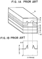
- Fig. 1A is a diagram showing a perspective view of a conventional semiconductor laser diode
- Fig. 1B shows a composition ratio of (Al+Ga)/In contained in a current blocking layer.
- the current blocking layer 11 is constituted by n-AlGaInP.
- a multiquantum-well (MQW) active layer 4 is sandwiched between an upper AlGaInP cladding layer 5 and a lower AlGaInP cladding layer 3, and there are provided a double heterostructure in which the upper cladding layer 5 is formed in a mesa stripe shape and a current blocking layer 11 which selectively buries the mesa side and bottom surfaces of the upper cladding layer 5.
- MQW multiquantum-well
- the numeral 1 depicts an n-GaAs substrate
- 2 depicts an n-GaAs buffer layer
- 6 depicts a p-GaInP cap layer
- 8 depicts a p-GaAs contact layer
- 9 depicts a p-electrode
- 10 depicts an n-electrode.
- the current blocking layer 11 of n-AlGaInP is selectively grown by an ordinary metalorganic vapor phase epitaxy method (MOVPE) without hydrogen chloride (HCl) being added.
- MOVPE metalorganic vapor phase epitaxy method
- an AlGaAs selective growth method using HCl is known as a method for selectively etching an AlGaAs layer of a material system which also includes aluminum (Al). This has been disclosed by researchers of Mitsubishi Kasei Corp. in Journal of Crystal Growth, Vol. 124, pp. 235-242, 1992. This method is intended to enhance the degree of selective growth of AlGaAs by adding HCl in carrying out the MOVPE process.
- composition ratio deviation occurs at the sides of the mesa is thought to be probably due to diffusion coefficient differences in various materials on a selective mask. It is thought that, on the selective mask, the diffusion coefficient of each of the Al and Ga source materials is larger than that of the In source material, resulting in a large deviation of the (A1+Ga)/In composition ratio from "1" at the mesa side portions.
- composition ratio deviation explained above has a good correlation with protrusions in the current blocking layer that are formed at the sides of the mesa as seen in Fig. 1A.
- the material on the selective mask diffuses at the mesa side portions during the growth and the protrusions result from an increased growth rate thereof at the mesa side portions as compared with that at the flat portion.
- An object of the present invention is to overcome the problem existing in the prior art and to provide a ridged type semiconductor laser diode and a method for fabricating the same, which is made highly reliable due to the reduction of stresses at mesa side portions caused by a composition ratio deviation in a current blocking layer.
- a semiconductor laser diode having: an active layer; a first and a second cladding layer sandwiching the active layer, the second cladding layer being in a double heterostructure formed in a mesa stripe form; a current blocking layer which is disposed at a side opposite from a substrate with respect to the active layer and which selectively buries mesa side and bottom surfaces of the first cladding layer, the semiconductor laser diode being characterized in that a protrusion formed in the current blocking layer at each of the mesa side surfaces has a thickness not larger than 10% of a thickness of the current blocking layer at its flat portion.
- a method for fabricating a semiconductor laser diode comprising the steps of: a first step of growing, sequentially above a substrate, a second cladding layer, an active layer, a first cladding layer and a cap layer; a second step of etching the first cladding layer and the cap layer respectively in mesa stripe forms; a third step of selectively growing a current blocking layer on the first cladding layer by a metalorganic vapor phase epitaxy process; and a fourth step of growing contact layers respectively on surfaces of the current blocking layer and the cap layer, the method being characterized in that the third step of selective growth is carried out by using a gas in which HCl is mixed in a concentration within a range of 0.2 ⁇ 2 in a (HCl)/(III gas) ratio.
- the composition ratio deviation occurs at the sides of the mesa due to diffusion coefficient differences in various materials on a selective mask and that the diffusion coefficient of the Al and Ga material is larger than that of the In material, resulting in a large deviation of the (A1+Ga)/In composition ratio from "1" at the mesa side portions thereby adversely affecting the reliability of the structure. It is also thought that the composition ratio deviation has a good correlation with protrusions in the current blocking layer that are formed at the mesa side portions and that, due to the diffusion of the material on the selective mask at the mesa side portions during the growth, the protrusions result from a faster growth of the material at the mesa side portions than at the flat portion.
- the re-evaporation of material on the selective mask may be enhanced so that the current blocking layer does not protrude at the mesa side portions.
- a first method is one in which parameters are changed in an MOVPE growth process. Specifically, if the growth is carried out under a reduced pressure, for example, an ultra low pressure in the order of 1 torr, the reevaporation of the material which diffuses on the selective mask is enhanced and the formation of protrusions of the n-AlGaInP current blocking layer which is a buried layer at the mesa side portions are suppressed and, as a result, the stress is also reduced.
- a reduced pressure for example, an ultra low pressure in the order of 1 torr
- a first step is to grow, sequentially above a substrate, a second cladding layer 3, an active layer 4, a first cladding layer 5 and a cap layer 6.
- a second step is to etch the first cladding layer 5 and the cap layer 6 respectively in mesa stripe forms. In this step, the etching is carried out to an intermediate point of the first cladding layer 5 in order to form an optical waveguide.
- a third step is to selectively grow a current blocking layer 7 on the first cladding layer 5 by a metalorganic vapor phase epitaxy (MOVPE) process.
- the materials used in this step are metalorganics and a gas in which a PH3 gas together with HCl is mixed in a concentration within a range of 0.2 ⁇ 2 in a (HCl)/III gas) ratio.
- a fourth step is to grow contact layers respectively on surfaces of the current blocking layer (7) and the cap layer (6).
- the current blocking layer when the current blocking layer is selectively grown by the MOVPE process, the reevaporation of the material on the selective mask is enhanced and, as a result, a protrusion formed in the current blocking layer at each of the mesa side surfaces can be made less than 10% of the thickness of the current blocking layer at its flat portion.
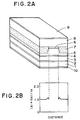
- Fig. 2A shows in a perspective view a structure of a first embodiment of the invention.
- Fig. 2B shows a composition ratio of (Al+Ga)/In contained in a current blocking layer.
- AlGaInP material system when (Al+Ga)/In is about "1", it is lattice-matched to GaAs of the substrate so that there is no occurrence of stress but, when (Al+Ga)/In largely deviates from "1", the lattice mismatch becomes large resulting in a large stress to the active layer.
- the numeral 1 depicts an n-GaAs substrate
- 2 depicts an n-GaAs buffer layer
- 3 depicts an n-AlGaInP cladding layer
- 4 depicts a multiquantum well (MQW) active layer
- 5 depicts a p-AlGaInP cladding layer
- 6 depicts a p-GaInP cap layer
- 7 depicts an n-AlGaInP current blocking layer
- 8 depicts a p-GaAs contact layer
- 9 depicts a p-electrode
- 10 depicts an n-electrode.
- the semiconductor laser diode of this embodiment is configured such that the MQW active layer 4 is sandwiched from above and below by the AlGaInP cladding layers 5 and 3, the upper cladding layer 5 is in a double heterostructure shaped in a mesa stripe form, and the current blocking layer 7 selectively buries mesa side and bottom surfaces of the upper cladding layer 5, wherein the feature resides in the fact that the thickness of a protrusion formed in the current blocking layer 7 at each of said mesa side surfaces is not larger than 10% of the thickness of the current blocking layer 7 at its flat portion.
- This semiconductor laser diode is fabricated by carrying out an MOVPE growth process three times, including a selective MOVPE growth process which is carried out once. All of these MOVPE growth processes are reduced pressure growth processes with the pressure being 76 torr. Also, the growth temperatures are all at 700°C.
- the first step is to grow, sequentially above an n-GaAs substrate 1, an n-GaAs buffer layer 2, an n-AlGaInP cladding layer 3, an MQW active layer 4, a p-AlGaInP cladding layer 5 and a p-GaInP cap layer 6, thereby forming a double heterostructure including the MQW active layer 4.
- the MQW active layer 4 includes 8 well layers each having a thickness of 8 nm. The oscillating wavelength is targeted to about 670 nm.
- a mask pattern of a stripe shape is formed on the cap layer 6 by a photolithography process.
- This mask uses a silicon nitride (SiN x ) film deposited by a plasma-assisted CVD process.
- SiN x silicon nitride
- the p-AlGaInP cladding layer 5 and the cap layer 6 are etched into mesa stripe forms.
- This etching is a wet etching of a sulfuric acid type and, for forming an optical waveguide, is stopped at an intermediate point to the cladding layer 5 as seen in Fig. 3B.
- the n-AlGaInP current blocking layer 7 is selectively grown as shown in Fig. 3C.
- the mixed crystal ratio is (Al 0.85 Ga 0.15 ) 0.5 In 0.5 P and the n-AlGaInP is transparent to the oscillation light, and it is so designed that the laser becomes a real refractive index guide.
- the materials used for this selective growth are metalorganics of TMAl, TEGa, TMIn, and a gas in which a PH3 gas and a HCl gas are mixed. In this case, the concentration of HCl is "1" in a mole ratio of (HCl)/(III gas).
- the concentration of HCl in the mixed gas used in the selective growth of the above n-AlGaInP current blocking layer 7 is most suitable in a range from "0.2" to "2" in the mole notation. It has been confirmed that, when the concentration is below that range, the composition ratio deviation at mesa side portions becomes somewhat large and, when the concentration is conversely above that range, there appears a gradual surface morphology deterioration of the n-AlGaInP current blocking layer 7 which is due to excess HCl.
- the protrusions formed at the mesa side portions are small as shown in Figs. 2A and 3C, thereby enabling the buried growth of the n-AlGaInP current blocking layer 7 in which the composition ratio deviation is small.
- the selective mask described above is removed, and the p-GaAs contact layer 8 is grown to a predetermined thickness by a third MOVPE growth as shown in Fig. 3D.
- the p-electrode 9 and the n-electrode 10 are formed respectively on an upper surface of the contact layer 8 and a bottom surface of the substrate 1.
- a Ti/Pt/Au electrode is vacuum-deposited on the contact layer 8 and heat-treated whereby the electrode 9 is formed, after which an upper surface of the substrate 1 is polished to some extent while the p-electrode 9 is being protected, and then an Au/Ge/Ni electrode is vacuum-deposited on the substrate 1 and heat-treated whereby the n-electrode 10 is formed.
- the fabrication of the semiconductor laser diode of this embodiment is completed.
- the thickness of the protrusions formed at the mesa side portions of the n-AlGaInP current blocking layer 7 is suppressed to a thickness less than 5% of the thickness of the n-AlGaInP current blocking layer 7 at its flat portion.
- the composition ratio of (Al+Ga)/In in the n-AlGaInP current blocking layer 7 is "1.05" and, when this value is compared with "1.5" in the conventional example, it is noted that the suppression is quite significant.
- the stress to the MQW active layer 4 is significantly reduced.
- the composition ratio deviation in the current blocking layer 7 at the mesa side portions can be suppressed to below "1.05".
- the semiconductor laser diode of the embodiment of the invention and a conventional semiconductor laser diode which has been fabricated by selective growth without HCl being added are compared by subjecting them to an electrical testing under the conditions of 50°C and 3 mW.
- the measurement of the composition has been carried out by EDX.
- the concentration of HCl contained in the mixed gas used in the selective growth of the n-AlGaInP current blocking layer 7 is "1" in the mole notation.
- the thickness of the protrusions at the mesa side portions can be suppressed to a thickness less than 10% of the thickness of the n-AlGaInP current blocking layer 7 at its flat portion.
- the AlGaInP visible light semiconductor laser is configured such that it is buried in the n-AlGaInP current blocking layer 7.
- the invention is not limited to that configuration since, for example, the structure may well be such that AlInP is included as the current blocking layer 7 or that GaInP is included in the active layer 4, or such that a 0.98 ⁇ 1.02 ⁇ m band laser which uses InGaAs for an active layer is buried in the current blocking layer containing GaInP, AlGaInP or AlInP.
- the thickness of the protrusions in the current blocking layer at the mesa side portions of the semiconductor laser diode is less than 10% of the thickness of the current blocking layer at its flat portion, it is possible to suppress the stress to be caused by the lattice mismatch at the mesa side portions, resulting in the enhancement of the reliability of the semiconductor laser diode.
- the stencil layer is first formed on the uppermost surface of the mesa forming region and then the stencil layer thus formed is removed by etching thereby removing a stacked layer grown on the surface of the mesa region so as to flatten this surface, the method according to the invention requires lesser number of steps to the extent that it does not require the formation and the removal of the stencil layer.
Landscapes
- Physics & Mathematics (AREA)
- Optics & Photonics (AREA)
- Nanotechnology (AREA)
- Engineering & Computer Science (AREA)
- Chemical & Material Sciences (AREA)
- General Physics & Mathematics (AREA)
- Life Sciences & Earth Sciences (AREA)
- Biophysics (AREA)
- Electromagnetism (AREA)
- Condensed Matter Physics & Semiconductors (AREA)
- Crystallography & Structural Chemistry (AREA)
- Geometry (AREA)
- Semiconductor Lasers (AREA)
Applications Claiming Priority (2)
| Application Number | Priority Date | Filing Date | Title |
|---|---|---|---|
| JP5341316A JP2822868B2 (ja) | 1993-12-10 | 1993-12-10 | 半導体レーザの製造方法 |
| JP341316/93 | 1993-12-10 |
Publications (3)
| Publication Number | Publication Date |
|---|---|
| EP0657977A2 true EP0657977A2 (de) | 1995-06-14 |
| EP0657977A3 EP0657977A3 (de) | 1995-12-27 |
| EP0657977B1 EP0657977B1 (de) | 1997-07-23 |
Family
ID=18345119
Family Applications (1)
| Application Number | Title | Priority Date | Filing Date |
|---|---|---|---|
| EP94119425A Expired - Lifetime EP0657977B1 (de) | 1993-12-10 | 1994-12-08 | Laser mit Streifenstruktur und Herstellungsverfahren |
Country Status (4)
| Country | Link |
|---|---|
| US (1) | US5478775A (de) |
| EP (1) | EP0657977B1 (de) |
| JP (1) | JP2822868B2 (de) |
| DE (1) | DE69404432T2 (de) |
Cited By (1)
| Publication number | Priority date | Publication date | Assignee | Title |
|---|---|---|---|---|
| CN103119808A (zh) * | 2010-09-28 | 2013-05-22 | 奥斯兰姆奥普托半导体有限责任公司 | 边缘发射的半导体激光二极管及其制造方法 |
Families Citing this family (7)
| Publication number | Priority date | Publication date | Assignee | Title |
|---|---|---|---|---|
| US6026106A (en) * | 1997-03-26 | 2000-02-15 | Mitsubishi Denki Kabushiki Kaisha | Composite optical device |
| JP3672062B2 (ja) * | 1997-07-16 | 2005-07-13 | 三菱電機株式会社 | 半導体レーザ,及びその製造方法 |
| JP3267582B2 (ja) | 1999-06-17 | 2002-03-18 | 日本電気株式会社 | 半導体レーザの製造方法 |
| KR101020387B1 (ko) | 2002-12-20 | 2011-03-08 | 크리 인코포레이티드 | 반도체 메사 구조와 도전형 접합을 포함하는 전자 소자 및그 제조방법 |
| KR100558437B1 (ko) * | 2003-06-24 | 2006-03-10 | 삼성전기주식회사 | 반도체 레이저의 제조방법 |
| JP2005085977A (ja) * | 2003-09-09 | 2005-03-31 | Sharp Corp | 半導体レーザ素子および半導体レーザ素子の製造方法 |
| US8487354B2 (en) * | 2009-08-21 | 2013-07-16 | Taiwan Semiconductor Manufacturing Company, Ltd. | Method for improving selectivity of epi process |
Family Cites Families (21)
| Publication number | Priority date | Publication date | Assignee | Title |
|---|---|---|---|---|
| US4213805A (en) * | 1973-05-28 | 1980-07-22 | Hitachi, Ltd. | Liquid phase epitaxy method of forming a filimentary laser device |
| US4147571A (en) * | 1977-07-11 | 1979-04-03 | Hewlett-Packard Company | Method for vapor epitaxial deposition of III/V materials utilizing organometallic compounds and a halogen or halide in a hot wall system |
| DE3105786A1 (de) * | 1981-02-17 | 1982-09-02 | Siemens AG, 1000 Berlin und 8000 München | Herstellung von lumineszenz- oder laserdioden mit intern begrenzter leuchtflaeche |
| JPS6050983A (ja) * | 1983-08-30 | 1985-03-22 | Sharp Corp | 半導体レ−ザ素子の製造方法 |
| JPS61180493A (ja) * | 1985-02-05 | 1986-08-13 | Matsushita Electric Ind Co Ltd | 半導体レ−ザ素子の製造方法 |
| JPH0710019B2 (ja) * | 1987-01-17 | 1995-02-01 | 日本電信電話株式会社 | 埋込み構造半導体レ−ザの製造方法 |
| JPH01175727A (ja) * | 1987-12-29 | 1989-07-12 | Nec Corp | 3−v族化合物半導体の選択埋め込み成長方法 |
| JPH0231487A (ja) * | 1988-07-20 | 1990-02-01 | Mitsubishi Electric Corp | 半導体レーザ装置とその製造方法 |
| US5173447A (en) * | 1989-10-31 | 1992-12-22 | The Furukawa Electric Co., Ltd. | Method for producing strained quantum well semiconductor laser elements |
| JPH03161987A (ja) * | 1989-11-20 | 1991-07-11 | Sanyo Electric Co Ltd | 半導体レーザ装置 |
| JP2549182B2 (ja) * | 1990-01-05 | 1996-10-30 | 住友電気工業株式会社 | 半導体レーザ素子 |
| US5268328A (en) * | 1990-09-07 | 1993-12-07 | Matsushita Electric Industrial Co., Ltd. | Method of fabricating a semiconductor laser |
| US5210767A (en) * | 1990-09-20 | 1993-05-11 | Mitsubishi Denki Kabushiki Kaisha | Semiconductor laser |
| FR2667197B1 (fr) * | 1990-09-20 | 1993-12-24 | Rosette Azoulay | Procede d'epitaxie selective et de gravure de materiau iii-v ou ii-vi dans un meme bati de croissance omcvd. |
| JPH04154184A (ja) * | 1990-10-18 | 1992-05-27 | Nec Corp | 半導体レーザ装置とその製造方法 |
| WO1993001614A1 (fr) * | 1991-07-05 | 1993-01-21 | Mitsubishi Kasei Corporation | Semi-conducteur a jonction et procede de fabrication correspondant |
| JP3129779B2 (ja) * | 1991-08-30 | 2001-01-31 | 株式会社東芝 | 半導体レーザ装置 |
| JPH05291683A (ja) * | 1992-04-10 | 1993-11-05 | Fujitsu Ltd | 半導体発光素子及びその製造方法 |
| JPH0697569A (ja) * | 1992-09-14 | 1994-04-08 | Fujitsu Ltd | 半導体レーザの製造方法 |
| JP3444610B2 (ja) * | 1992-09-29 | 2003-09-08 | 三菱化学株式会社 | 半導体レーザ装置 |
| JPH0750445A (ja) * | 1993-06-02 | 1995-02-21 | Rohm Co Ltd | 半導体レーザの製法 |
-
1993
- 1993-12-10 JP JP5341316A patent/JP2822868B2/ja not_active Expired - Fee Related
-
1994
- 1994-12-07 US US08/350,886 patent/US5478775A/en not_active Expired - Lifetime
- 1994-12-08 EP EP94119425A patent/EP0657977B1/de not_active Expired - Lifetime
- 1994-12-08 DE DE69404432T patent/DE69404432T2/de not_active Expired - Fee Related
Cited By (3)
| Publication number | Priority date | Publication date | Assignee | Title |
|---|---|---|---|---|
| CN103119808A (zh) * | 2010-09-28 | 2013-05-22 | 奥斯兰姆奥普托半导体有限责任公司 | 边缘发射的半导体激光二极管及其制造方法 |
| US8995490B2 (en) | 2010-09-28 | 2015-03-31 | Osram Opto Semiconductors Gmbh | Edge-emitting semiconductor laser diode and method for producing the same |
| CN103119808B (zh) * | 2010-09-28 | 2015-08-19 | 奥斯兰姆奥普托半导体有限责任公司 | 边缘发射的半导体激光二极管及其制造方法 |
Also Published As
| Publication number | Publication date |
|---|---|
| DE69404432D1 (de) | 1997-08-28 |
| EP0657977A3 (de) | 1995-12-27 |
| JP2822868B2 (ja) | 1998-11-11 |
| EP0657977B1 (de) | 1997-07-23 |
| US5478775A (en) | 1995-12-26 |
| JPH07162093A (ja) | 1995-06-23 |
| DE69404432T2 (de) | 1998-02-26 |
Similar Documents
| Publication | Publication Date | Title |
|---|---|---|
| EP0661782B1 (de) | Halbleiterlaser | |
| EP0552888B1 (de) | Mittels MOCVD auf einem strukturiertem Substrat aufgewachsene Laser mit vergrabener Heterostruktur | |
| JPH10126010A (ja) | 半導体レーザ装置の製造方法 | |
| US5633886A (en) | Short wavelength VCSEL with Al-free active region | |
| EP0526128B1 (de) | Verfahren zur Herstellung eines Halbleiterlasers mit verteilter Rückkoppelung | |
| EP0503211B1 (de) | Halbleiteranordnung mit einer auf einem strukturierten Substrat aufgewachsenen Schichtstruktur | |
| EP0177221B1 (de) | Halbleiterlaser | |
| US5336635A (en) | Manufacturing method of semiconductor laser of patterned-substrate type | |
| CA2076605A1 (en) | Algainp diodes emitting visible light | |
| EP0209387B1 (de) | Halbleiterlaser-Vorrichtung | |
| EP0440471B1 (de) | Laserdiode mit stabilisiertem Transversal-Mode | |
| US4905246A (en) | Semiconductor laser device | |
| US5838028A (en) | Semiconductor device having a ridge or groove | |
| US5446753A (en) | Current block type semiconductor laser | |
| EP0657977B1 (de) | Laser mit Streifenstruktur und Herstellungsverfahren | |
| US6518159B1 (en) | Semiconductor laser device and a method for fabricating the same | |
| US5420066A (en) | Method for producing semiconductor laser device using etch stop layer | |
| US5379312A (en) | Semiconductor laser with tensile-strained etch-stop layer | |
| JP4028158B2 (ja) | 半導体光デバイス装置 | |
| US5304507A (en) | Process for manufacturing semiconductor laser having low oscillation threshold current | |
| JP3022351B2 (ja) | 光半導体装置及びその製造方法 | |
| JP2003152282A (ja) | 半導体レーザ素子 | |
| US6668002B2 (en) | Semiconductor laser device including ARROW structure formed without P-As interdiffusion and Al oxidation | |
| JP2003332691A (ja) | 半導体レーザ素子およびその製造方法 | |
| JPH04307781A (ja) | 半導体レーザ |
Legal Events
| Date | Code | Title | Description |
|---|---|---|---|
| PUAI | Public reference made under article 153(3) epc to a published international application that has entered the european phase |
Free format text: ORIGINAL CODE: 0009012 |
|
| AK | Designated contracting states |
Kind code of ref document: A2 Designated state(s): DE GB NL |
|
| PUAL | Search report despatched |
Free format text: ORIGINAL CODE: 0009013 |
|
| AK | Designated contracting states |
Kind code of ref document: A3 Designated state(s): DE GB NL |
|
| 17P | Request for examination filed |
Effective date: 19951113 |
|
| 17Q | First examination report despatched |
Effective date: 19960430 |
|
| GRAG | Despatch of communication of intention to grant |
Free format text: ORIGINAL CODE: EPIDOS AGRA |
|
| GRAH | Despatch of communication of intention to grant a patent |
Free format text: ORIGINAL CODE: EPIDOS IGRA |
|
| GRAH | Despatch of communication of intention to grant a patent |
Free format text: ORIGINAL CODE: EPIDOS IGRA |
|
| GRAA | (expected) grant |
Free format text: ORIGINAL CODE: 0009210 |
|
| AK | Designated contracting states |
Kind code of ref document: B1 Designated state(s): DE GB NL |
|
| REF | Corresponds to: |
Ref document number: 69404432 Country of ref document: DE Date of ref document: 19970828 |
|
| PLBE | No opposition filed within time limit |
Free format text: ORIGINAL CODE: 0009261 |
|
| STAA | Information on the status of an ep patent application or granted ep patent |
Free format text: STATUS: NO OPPOSITION FILED WITHIN TIME LIMIT |
|
| 26N | No opposition filed | ||
| REG | Reference to a national code |
Ref country code: GB Ref legal event code: IF02 |
|
| REG | Reference to a national code |
Ref country code: GB Ref legal event code: 732E |
|
| NLS | Nl: assignments of ep-patents |
Owner name: NEC COMPOUND SEMICONDUTOR DEVICES, LTD. |
|
| REG | Reference to a national code |
Ref country code: GB Ref legal event code: 732E |
|
| NLS | Nl: assignments of ep-patents |
Owner name: NEC ELECTRONICS CORPORATION Effective date: 20060404 |
|
| PGFP | Annual fee paid to national office [announced via postgrant information from national office to epo] |
Ref country code: NL Payment date: 20071216 Year of fee payment: 14 |
|
| PGFP | Annual fee paid to national office [announced via postgrant information from national office to epo] |
Ref country code: GB Payment date: 20071205 Year of fee payment: 14 |
|
| PGFP | Annual fee paid to national office [announced via postgrant information from national office to epo] |
Ref country code: DE Payment date: 20071206 Year of fee payment: 14 |
|
| GBPC | Gb: european patent ceased through non-payment of renewal fee |
Effective date: 20081208 |
|
| NLV4 | Nl: lapsed or anulled due to non-payment of the annual fee |
Effective date: 20090701 |
|
| PG25 | Lapsed in a contracting state [announced via postgrant information from national office to epo] |
Ref country code: DE Free format text: LAPSE BECAUSE OF NON-PAYMENT OF DUE FEES Effective date: 20090701 |
|
| PG25 | Lapsed in a contracting state [announced via postgrant information from national office to epo] |
Ref country code: NL Free format text: LAPSE BECAUSE OF NON-PAYMENT OF DUE FEES Effective date: 20090701 Ref country code: GB Free format text: LAPSE BECAUSE OF NON-PAYMENT OF DUE FEES Effective date: 20081208 |