EP0658927A1 - Procédé de formation d'une cavité en forme de parallélépipède destinée à accueillir un composant dans un support - Google Patents
Procédé de formation d'une cavité en forme de parallélépipède destinée à accueillir un composant dans un support Download PDFInfo
- Publication number
- EP0658927A1 EP0658927A1 EP94116892A EP94116892A EP0658927A1 EP 0658927 A1 EP0658927 A1 EP 0658927A1 EP 94116892 A EP94116892 A EP 94116892A EP 94116892 A EP94116892 A EP 94116892A EP 0658927 A1 EP0658927 A1 EP 0658927A1
- Authority
- EP
- European Patent Office
- Prior art keywords
- component
- window
- recess
- support plate
- receiving
- Prior art date
- Legal status (The legal status is an assumption and is not a legal conclusion. Google has not performed a legal analysis and makes no representation as to the accuracy of the status listed.)
- Withdrawn
Links
Images
Classifications
-
- H—ELECTRICITY
- H10—SEMICONDUCTOR DEVICES; ELECTRIC SOLID-STATE DEVICES NOT OTHERWISE PROVIDED FOR
- H10W—GENERIC PACKAGES, INTERCONNECTIONS, CONNECTORS OR OTHER CONSTRUCTIONAL DETAILS OF DEVICES COVERED BY CLASS H10
- H10W70/00—Package substrates; Interposers; Redistribution layers [RDL]
- H10W70/60—Insulating or insulated package substrates; Interposers; Redistribution layers
- H10W70/67—Insulating or insulated package substrates; Interposers; Redistribution layers characterised by their insulating layers or insulating parts
- H10W70/69—Insulating materials thereof
- H10W70/698—Semiconductor materials that are electrically insulating, e.g. undoped silicon
-
- H—ELECTRICITY
- H10—SEMICONDUCTOR DEVICES; ELECTRIC SOLID-STATE DEVICES NOT OTHERWISE PROVIDED FOR
- H10P—GENERIC PROCESSES OR APPARATUS FOR THE MANUFACTURE OR TREATMENT OF DEVICES COVERED BY CLASS H10
- H10P50/00—Etching of wafers, substrates or parts of devices
- H10P50/69—Etching of wafers, substrates or parts of devices using masks for semiconductor materials
- H10P50/691—Etching of wafers, substrates or parts of devices using masks for semiconductor materials for Group V materials or Group III-V materials
- H10P50/693—Etching of wafers, substrates or parts of devices using masks for semiconductor materials for Group V materials or Group III-V materials characterised by their size, orientation, disposition, behaviour or shape, in horizontal or vertical plane
-
- H—ELECTRICITY
- H10—SEMICONDUCTOR DEVICES; ELECTRIC SOLID-STATE DEVICES NOT OTHERWISE PROVIDED FOR
- H10W—GENERIC PACKAGES, INTERCONNECTIONS, CONNECTORS OR OTHER CONSTRUCTIONAL DETAILS OF DEVICES COVERED BY CLASS H10
- H10W70/00—Package substrates; Interposers; Redistribution layers [RDL]
- H10W70/01—Manufacture or treatment
- H10W70/05—Manufacture or treatment of insulating or insulated package substrates, or of interposers, or of redistribution layers
- H10W70/08—Manufacture or treatment of insulating or insulated package substrates, or of interposers, or of redistribution layers by depositing layers on the chip or wafer, e.g. "chip-first" RDLs
- H10W70/09—Manufacture or treatment of insulating or insulated package substrates, or of interposers, or of redistribution layers by depositing layers on the chip or wafer, e.g. "chip-first" RDLs extending onto an encapsulation that laterally surrounds the chip or wafer, e.g. fan-out wafer level package [FOWLP] RDLs
-
- H—ELECTRICITY
- H10—SEMICONDUCTOR DEVICES; ELECTRIC SOLID-STATE DEVICES NOT OTHERWISE PROVIDED FOR
- H10W—GENERIC PACKAGES, INTERCONNECTIONS, CONNECTORS OR OTHER CONSTRUCTIONAL DETAILS OF DEVICES COVERED BY CLASS H10
- H10W70/00—Package substrates; Interposers; Redistribution layers [RDL]
- H10W70/60—Insulating or insulated package substrates; Interposers; Redistribution layers
- H10W70/67—Insulating or insulated package substrates; Interposers; Redistribution layers characterised by their insulating layers or insulating parts
- H10W70/68—Shapes or dispositions thereof
-
- H—ELECTRICITY
- H10—SEMICONDUCTOR DEVICES; ELECTRIC SOLID-STATE DEVICES NOT OTHERWISE PROVIDED FOR
- H10W—GENERIC PACKAGES, INTERCONNECTIONS, CONNECTORS OR OTHER CONSTRUCTIONAL DETAILS OF DEVICES COVERED BY CLASS H10
- H10W99/00—Subject matter not provided for in other groups of this subclass
-
- H—ELECTRICITY
- H10—SEMICONDUCTOR DEVICES; ELECTRIC SOLID-STATE DEVICES NOT OTHERWISE PROVIDED FOR
- H10W—GENERIC PACKAGES, INTERCONNECTIONS, CONNECTORS OR OTHER CONSTRUCTIONAL DETAILS OF DEVICES COVERED BY CLASS H10
- H10W70/00—Package substrates; Interposers; Redistribution layers [RDL]
- H10W70/60—Insulating or insulated package substrates; Interposers; Redistribution layers
-
- H—ELECTRICITY
- H10—SEMICONDUCTOR DEVICES; ELECTRIC SOLID-STATE DEVICES NOT OTHERWISE PROVIDED FOR
- H10W—GENERIC PACKAGES, INTERCONNECTIONS, CONNECTORS OR OTHER CONSTRUCTIONAL DETAILS OF DEVICES COVERED BY CLASS H10
- H10W72/00—Interconnections or connectors in packages
- H10W72/90—Bond pads, in general
- H10W72/941—Dispositions of bond pads
- H10W72/9413—Dispositions of bond pads on encapsulations
Definitions
- the invention relates to a method for producing a rectangular recess for receiving a component in a carrier plate.
- MCM multi-chip module technology
- An electrical connection of the components above the level of the component surfaces by means of electrical conductor tracks is advantageous.
- a layer of insulating material can be for example, polyimide, which carries the conductor tracks, the area of the underlying components can also be used.
- the object of the present invention is to produce cuboid depressions for receiving components in carrier plates, which are exactly adapted to the components to be accommodated with regard to their lateral and vertical dimensions.
- a mask with at least one rectangular window is arranged on a silicon wafer, the surface of which lies in the (100) plane, the sides of the window being aligned parallel to ⁇ 100> directions and the side lengths are smaller by a predetermined value than the intended edge lengths of the depression, and that anisotropic etching takes place until the edges of the depression reach the predetermined length. It is preferably provided in the method according to the invention that the predetermined value corresponds to twice the intended depth of the depression.
- An advantage of the method according to the invention is that the intended dimensions of the recess can be achieved very precisely. Furthermore, the walls of the depression are vertical, so that no prismatic gap remains between the component and the wall of the depression, which makes it difficult or even impossible to apply a carrier layer for the conductor tracks.
- the carrier plate made of silicon is characterized by a high level of flatness, a value for money and the fact that it can be processed with the means of integrated circuit technology.
- a silicon wafer is used, the surface of which lies in the (100) plane.
- the window of the mask for creating the depression is not, as is customary, aligned with the edges parallel to the ⁇ 110> direction, which is usually characterized by a flattening (flat) on the edge of the wafer, but at 45 ° to it marked direction. This is a ⁇ 100> direction.
- anisotropic etching with masks the window edges of which are aligned parallel to the ⁇ 110> direction, there is no self-stop of the etching process when a difficultly etching (111) plane is reached. Rather, the etching process continues indefinitely.
- the anisotropic etching of the silicon is based on the dependence of the etching speed on the crystallographic direction.
- the etching rate is approximately 100 times lower than in the ⁇ 133> direction in which the maximum etching rate is reached.
- there is a secondary minimum in the etching rate which is in the ⁇ 100> direction.
- this ⁇ 100> secondary minimum is nowhere near as pronounced as the main minimum in the ⁇ 111> direction.
- the etching speed in the ⁇ 100> direction only decreases to approximately 75% of its maximum value in the ⁇ 133> direction.
- the etching process does not come to a standstill on a (100) plane, the reduction in the etching speed at the minimum means that all (100) planes are formed as very smooth surfaces during the etching process.
- the side walls are set back from the mask edges by the same amount as the etching progresses in depth. This finding is the basis of the invention.
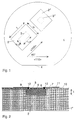
- the wafer 1 made of silicon shown in FIG. 1 is to be provided with depressions 2, 2 'using the method according to the invention.
- the window 3 has the dimensions 1 m and b m , for example. Because the etching proceeds not only perpendicularly to the surface of the wafer 1, but also parallel to it, the dimensions 1 and b for the recess 2 then result.
- the flat 4 provided on each wafer for the purpose of alignment is in the ⁇ 100 > Direction, which forms an angle of 45 ° to the ⁇ 110> direction and thus to the direction of the respective edges of the depressions 2, 2 '.
- the depression 2 is etched into the carrier 1 ′ made from the wafer 1 (FIG. 1) with the depth t.
- a component (semiconductor chip) 5 is inserted into this recess and fastened to the bottom 6 of the recess in a known manner by soldering or gluing.
- the side walls 7 of the recess 2 form with the side walls 8 of the component 5 a very narrow and parallel gap, which can preferably be filled with a heat-conducting adhesive.
- An insulating carrier layer 10, which carries the conductor tracks 11, is applied to the surface of the carrier 1 ′ and the component 5. These are connected to the connection surfaces of the component 5 via plated-through holes 12.
Landscapes
- Drying Of Semiconductors (AREA)
- Weting (AREA)
Applications Claiming Priority (2)
| Application Number | Priority Date | Filing Date | Title |
|---|---|---|---|
| DE4342767 | 1993-12-15 | ||
| DE4342767A DE4342767A1 (de) | 1993-12-15 | 1993-12-15 | Verfahren zur Herstellung einer quaderförmigen Vertiefung zur Aufnahme eines Bauelementes in einer Trägerplatte |
Publications (1)
| Publication Number | Publication Date |
|---|---|
| EP0658927A1 true EP0658927A1 (fr) | 1995-06-21 |
Family
ID=6505078
Family Applications (1)
| Application Number | Title | Priority Date | Filing Date |
|---|---|---|---|
| EP94116892A Withdrawn EP0658927A1 (fr) | 1993-12-15 | 1994-10-26 | Procédé de formation d'une cavité en forme de parallélépipède destinée à accueillir un composant dans un support |
Country Status (2)
| Country | Link |
|---|---|
| EP (1) | EP0658927A1 (fr) |
| DE (1) | DE4342767A1 (fr) |
Cited By (9)
| Publication number | Priority date | Publication date | Assignee | Title |
|---|---|---|---|---|
| DE19900803A1 (de) * | 1999-01-12 | 2000-07-20 | Siemens Ag | Integrierter Schaltkreis |
| EP1130631A1 (fr) | 2000-02-29 | 2001-09-05 | STMicroelectronics S.r.l. | Procédé de fabrication d'une cavité enterrée dans une plaqette semi-conductrice |
| EP1195352A1 (fr) * | 2000-10-09 | 2002-04-10 | Interuniversitair Micro-Elektronica Centrum | Procédé de fabrication de composants micro-usinés et composants ainsi fabriqués |
| EP0678920B1 (fr) * | 1994-04-20 | 2003-01-29 | GENERAL SEMICONDUCTOR, Inc. | Dispositif semi-conducteur à structure de mesa |
| FR2831327A1 (fr) * | 2001-10-22 | 2003-04-25 | Commissariat Energie Atomique | Composant micro ou nano-electronique comportant une source d'energie et des moyens de protection de la source d'energie |
| US6740542B2 (en) | 2000-10-09 | 2004-05-25 | Interuniversitair Microelektronica Centrum | Method for producing micromachined devices and devices obtained thereof |
| EP1346615A4 (fr) * | 2000-10-20 | 2006-02-01 | Silverbrook Res Pty Ltd | Support circuits integres plusieurs microcircuits |
| EP1410701A4 (fr) * | 2000-10-20 | 2006-03-22 | Silverbrook Res Pty Ltd | Procede de fabrication d'un support de circuit integre |
| EP1201604A3 (fr) * | 2000-10-09 | 2006-04-12 | Interuniversitair Micro-Elektronica Centrum Vzw | Dispositifs micro-usinés et leur procédé de fabrication |
Families Citing this family (1)
| Publication number | Priority date | Publication date | Assignee | Title |
|---|---|---|---|---|
| DE10114956C2 (de) * | 2001-03-27 | 2003-06-18 | Infineon Technologies Ag | Verfahren zum Herstellen einer dielektrischen Schicht als Isolatorschicht für einen Grabenkondensator |
Citations (7)
| Publication number | Priority date | Publication date | Assignee | Title |
|---|---|---|---|---|
| DE2845062A1 (de) * | 1977-10-17 | 1979-04-19 | Hitachi Ltd | Halbleiteranordnung und verfahren zur herstellung einer halbleiteranordnung |
| JPS598375A (ja) * | 1982-07-05 | 1984-01-17 | Matsushita Electronics Corp | 縦型構造電界効果トランジスタ |
| EP0288052A2 (fr) * | 1987-04-21 | 1988-10-26 | Sumitomo Electric Industries Limited | Dispositif semi-conducteur comprenant un substrat et son procédé de fabrication |
| US4866501A (en) * | 1985-12-16 | 1989-09-12 | American Telephone And Telegraph Company At&T Bell Laboratories | Wafer scale integration |
| US4969359A (en) * | 1989-04-06 | 1990-11-13 | Ford Motor Company | Silicon accelerometer responsive to three orthogonal force components and method for fabricating |
| US5063177A (en) * | 1990-10-04 | 1991-11-05 | Comsat | Method of packaging microwave semiconductor components and integrated circuits |
| JPH05234901A (ja) * | 1992-02-19 | 1993-09-10 | Komatsu Ltd | 結晶成長方法 |
Family Cites Families (5)
| Publication number | Priority date | Publication date | Assignee | Title |
|---|---|---|---|---|
| US3986200A (en) * | 1974-01-02 | 1976-10-12 | Signetics Corporation | Semiconductor structure and method |
| DD272737A1 (de) * | 1988-05-18 | 1989-10-18 | Teltov Geraete Regler | Verfahren zur herstellung einer schmalen (100)-orientierten rechteckigen membran aus monokristallinem silizium |
| US4981552A (en) * | 1989-04-06 | 1991-01-01 | Ford Motor Company | Method for fabricating a silicon accelerometer responsive to three orthogonal force components |
| DE4106287A1 (de) * | 1990-10-25 | 1992-04-30 | Bosch Gmbh Robert | Verfahren zum anisotropen aetzen von monokristallinen, scheibenfoermigen traegern |
| DE9210198U1 (de) * | 1992-07-30 | 1992-10-15 | Meyerhoff, Dieter, 4010 Hilden | Chip-Modul |
-
1993
- 1993-12-15 DE DE4342767A patent/DE4342767A1/de not_active Ceased
-
1994
- 1994-10-26 EP EP94116892A patent/EP0658927A1/fr not_active Withdrawn
Patent Citations (7)
| Publication number | Priority date | Publication date | Assignee | Title |
|---|---|---|---|---|
| DE2845062A1 (de) * | 1977-10-17 | 1979-04-19 | Hitachi Ltd | Halbleiteranordnung und verfahren zur herstellung einer halbleiteranordnung |
| JPS598375A (ja) * | 1982-07-05 | 1984-01-17 | Matsushita Electronics Corp | 縦型構造電界効果トランジスタ |
| US4866501A (en) * | 1985-12-16 | 1989-09-12 | American Telephone And Telegraph Company At&T Bell Laboratories | Wafer scale integration |
| EP0288052A2 (fr) * | 1987-04-21 | 1988-10-26 | Sumitomo Electric Industries Limited | Dispositif semi-conducteur comprenant un substrat et son procédé de fabrication |
| US4969359A (en) * | 1989-04-06 | 1990-11-13 | Ford Motor Company | Silicon accelerometer responsive to three orthogonal force components and method for fabricating |
| US5063177A (en) * | 1990-10-04 | 1991-11-05 | Comsat | Method of packaging microwave semiconductor components and integrated circuits |
| JPH05234901A (ja) * | 1992-02-19 | 1993-09-10 | Komatsu Ltd | 結晶成長方法 |
Non-Patent Citations (3)
| Title |
|---|
| AKIRA KOIDE ET AL.: "Simulation of two-dimensional etch profile of silicon during orientation-dependent anisotropic etching", PROCEEDINGS IEEE MICRO ELECTRO MECHANICAL SYSTEMS, 30 January 1991 (1991-01-30), NARA, JAPAN, pages 216 - 220, XP000295571 * |
| PATENT ABSTRACTS OF JAPAN vol. 17, no. 683 (E - 1477) 15 December 1993 (1993-12-15) * |
| PATENT ABSTRACTS OF JAPAN vol. 8, no. 88 (E - 240) 21 April 1984 (1984-04-21) * |
Cited By (19)
| Publication number | Priority date | Publication date | Assignee | Title |
|---|---|---|---|---|
| EP0678920B1 (fr) * | 1994-04-20 | 2003-01-29 | GENERAL SEMICONDUCTOR, Inc. | Dispositif semi-conducteur à structure de mesa |
| DE19900803A1 (de) * | 1999-01-12 | 2000-07-20 | Siemens Ag | Integrierter Schaltkreis |
| US6992367B2 (en) | 2000-02-29 | 2006-01-31 | Stmicroelectronics, S.R.L. | Process for forming a buried cavity in a semiconductor material wafer and a buried cavity |
| EP1130631A1 (fr) | 2000-02-29 | 2001-09-05 | STMicroelectronics S.r.l. | Procédé de fabrication d'une cavité enterrée dans une plaqette semi-conductrice |
| US6693039B2 (en) | 2000-02-29 | 2004-02-17 | Stmicroelectronics S.R.L. | Process for forming a buried cavity in a semiconductor material wafer and a buried cavity |
| EP1195352A1 (fr) * | 2000-10-09 | 2002-04-10 | Interuniversitair Micro-Elektronica Centrum | Procédé de fabrication de composants micro-usinés et composants ainsi fabriqués |
| EP1201604A3 (fr) * | 2000-10-09 | 2006-04-12 | Interuniversitair Micro-Elektronica Centrum Vzw | Dispositifs micro-usinés et leur procédé de fabrication |
| US6740542B2 (en) | 2000-10-09 | 2004-05-25 | Interuniversitair Microelektronica Centrum | Method for producing micromachined devices and devices obtained thereof |
| US7247941B2 (en) | 2000-10-20 | 2007-07-24 | Silverbrook Research Pty Ltd | Printed circuit board assembly with strain-alleviating structures |
| EP1346615A4 (fr) * | 2000-10-20 | 2006-02-01 | Silverbrook Res Pty Ltd | Support circuits integres plusieurs microcircuits |
| EP1410701A4 (fr) * | 2000-10-20 | 2006-03-22 | Silverbrook Res Pty Ltd | Procede de fabrication d'un support de circuit integre |
| US7307354B2 (en) | 2000-10-20 | 2007-12-11 | Silverbrook Research Pty Ltd | Integrated circuit (IC) carrier assembly incorporating an integrated circuit (IC) retainer |
| US7402894B2 (en) | 2000-10-20 | 2008-07-22 | Silverbrook Research Pty Ltd | Integrated circuit carrier |
| US7479697B2 (en) | 2000-10-20 | 2009-01-20 | Silverbrook Research Pty Ltd | Resilient carrier assembly for an integrated circuit |
| US7705452B2 (en) | 2000-10-20 | 2010-04-27 | Silverbrook Research Pty Ltd | Carrier assembly for an integrated circuit |
| US7767912B2 (en) | 2000-10-20 | 2010-08-03 | Silverbrook Research Pty Ltd | Integrated circuit carrier arrangement with electrical connection islands |
| US7936063B2 (en) | 2000-10-20 | 2011-05-03 | Silverbrook Research Pty Ltd | Carrier assembly for an integrated circuit |
| WO2003036719A3 (fr) * | 2001-10-22 | 2004-03-04 | Commissariat Energie Atomique | Composant micro ou nano-electronique comportant une source d'energie et des moyens de protection de la source d'energie |
| FR2831327A1 (fr) * | 2001-10-22 | 2003-04-25 | Commissariat Energie Atomique | Composant micro ou nano-electronique comportant une source d'energie et des moyens de protection de la source d'energie |
Also Published As
| Publication number | Publication date |
|---|---|
| DE4342767A1 (de) | 1995-06-22 |
Similar Documents
| Publication | Publication Date | Title |
|---|---|---|
| DE69634877T2 (de) | Ein siliziumsubstrat mit einer ausnehmung zur aufnahme eines elements, und verfahren zur herstellung einer solchen ausnehmung | |
| DE60029962T2 (de) | Anordnung für die montage von chips auf leiterplatten | |
| DE3134110C2 (fr) | ||
| DE69331876T2 (de) | Ausrichtung von integrierten optischen Komponenten | |
| DE68917614T2 (de) | Verfahren zum Ausrichten und zur Herstellung eines Verbindungszapfens. | |
| DE3886882T2 (de) | Methode zur Ausbildung von Verbindungen zwischen leitenden Ebenen. | |
| DE3735455C2 (fr) | ||
| EP0078337B1 (fr) | Dispositif de contact pour la connexion amovible de composants électriques | |
| DE19713173A1 (de) | ROM-Speicher | |
| DE3531734A1 (de) | Einrichtung zur positionierung eines halbleiterlasers mit selbstjustierender wirkung fuer eine anzukoppelnde glasfaser | |
| DE2238450C3 (de) | Verfahren zur Herstellung einer integrierten Halbleiteranordnung | |
| DE2129132A1 (de) | Elektrische Schaltungsanordnung und Verfahren zu deren Herstellung | |
| DE4036093A1 (de) | Ic-modul | |
| DE2166754B2 (de) | Verschiebewerkzeug zum herstellen und trennen einer elektrischen steckkontaktverbindung | |
| EP1133795A1 (fr) | Procede de production d'un circuit integre traite sur ses deux faces | |
| DE19757269B4 (de) | Verfahren zur Herstellung eines Silicium-Auf-Isolator-Halbleitersubstrats | |
| DE2039988A1 (de) | Halbleiteranordnung und Verfahren zu ihrer Herstellung | |
| DE4342767A1 (de) | Verfahren zur Herstellung einer quaderförmigen Vertiefung zur Aufnahme eines Bauelementes in einer Trägerplatte | |
| DE19632103A1 (de) | Eingriffstörungsverhinderungszahnrad für Kommunikationsvorrichtungen und elektrische Geräte | |
| DE68914099T2 (de) | Flankenabschrägen von Löchern durch dielektrische Schichten zur Erzeugung von Kontakten in integrierten Schaltkreisen. | |
| DE2652870A1 (de) | Lasermatrixanordnung in planartechnik | |
| DE3787024T2 (de) | Herstellungsverfahren eines Mikrowellenüberganges zwischen zwei orthogonalen Leitungsstrukturen und Mikrowellenschaltung mit diesem Übergang. | |
| DE60037717T2 (de) | Datenträger mit integriertem schaltkreis und übertragungsspule | |
| DE10259792A1 (de) | Verfahren zum Herstellen einer Halbleitervorrichtung und Halbleitervorrichtung | |
| DE102007031549B4 (de) | Vorrichtung aus einkristallinem Silizium und Verfahren zur Herstellung einer Vorrichtung aus einkristallinem Silizium |
Legal Events
| Date | Code | Title | Description |
|---|---|---|---|
| PUAI | Public reference made under article 153(3) epc to a published international application that has entered the european phase |
Free format text: ORIGINAL CODE: 0009012 |
|
| AK | Designated contracting states |
Kind code of ref document: A1 Designated state(s): DE ES FR GB IT NL |
|
| 17P | Request for examination filed |
Effective date: 19951221 |
|
| RAP1 | Party data changed (applicant data changed or rights of an application transferred) |
Owner name: ROBERT BOSCH GMBH |
|
| 17Q | First examination report despatched |
Effective date: 19991208 |
|
| STAA | Information on the status of an ep patent application or granted ep patent |
Free format text: STATUS: THE APPLICATION IS DEEMED TO BE WITHDRAWN |
|
| 18D | Application deemed to be withdrawn |
Effective date: 20000620 |