EP0658957A2 - Connecteur électrique à haute densité - Google Patents
Connecteur électrique à haute densité Download PDFInfo
- Publication number
- EP0658957A2 EP0658957A2 EP94308195A EP94308195A EP0658957A2 EP 0658957 A2 EP0658957 A2 EP 0658957A2 EP 94308195 A EP94308195 A EP 94308195A EP 94308195 A EP94308195 A EP 94308195A EP 0658957 A2 EP0658957 A2 EP 0658957A2
- Authority
- EP
- European Patent Office
- Prior art keywords
- segments
- grooves
- high density
- electrical connector
- housing
- Prior art date
- Legal status (The legal status is an assumption and is not a legal conclusion. Google has not performed a legal analysis and makes no representation as to the accuracy of the status listed.)
- Withdrawn
Links
Images


Classifications
-
- H—ELECTRICITY
- H05—ELECTRIC TECHNIQUES NOT OTHERWISE PROVIDED FOR
- H05K—PRINTED CIRCUITS; CASINGS OR CONSTRUCTIONAL DETAILS OF ELECTRIC APPARATUS; MANUFACTURE OF ASSEMBLAGES OF ELECTRICAL COMPONENTS
- H05K7/00—Constructional details common to different types of electric apparatus
- H05K7/14—Mounting supporting structure in casing or on frame or rack
- H05K7/1438—Back panels or connecting means therefor; Terminals; Coding means to avoid wrong insertion
- H05K7/1439—Back panel mother boards
- H05K7/1441—Back panel mother boards with a segmented structure
-
- H—ELECTRICITY
- H01—ELECTRIC ELEMENTS
- H01R—ELECTRICALLY-CONDUCTIVE CONNECTIONS; STRUCTURAL ASSOCIATIONS OF A PLURALITY OF MUTUALLY-INSULATED ELECTRICAL CONNECTING ELEMENTS; COUPLING DEVICES; CURRENT COLLECTORS
- H01R12/00—Structural associations of a plurality of mutually-insulated electrical connecting elements, specially adapted for printed circuits, e.g. printed circuit boards [PCB], flat or ribbon cables, or like generally planar structures, e.g. terminal strips, terminal blocks; Coupling devices specially adapted for printed circuits, flat or ribbon cables, or like generally planar structures; Terminals specially adapted for contact with, or insertion into, printed circuits, flat or ribbon cables, or like generally planar structures
- H01R12/70—Coupling devices
- H01R12/71—Coupling devices for rigid printing circuits or like structures
- H01R12/712—Coupling devices for rigid printing circuits or like structures co-operating with the surface of the printed circuit or with a coupling device exclusively provided on the surface of the printed circuit
- H01R12/714—Coupling devices for rigid printing circuits or like structures co-operating with the surface of the printed circuit or with a coupling device exclusively provided on the surface of the printed circuit with contacts abutting directly the printed circuit; Button contacts therefore provided on the printed circuit
-
- H—ELECTRICITY
- H01—ELECTRIC ELEMENTS
- H01R—ELECTRICALLY-CONDUCTIVE CONNECTIONS; STRUCTURAL ASSOCIATIONS OF A PLURALITY OF MUTUALLY-INSULATED ELECTRICAL CONNECTING ELEMENTS; COUPLING DEVICES; CURRENT COLLECTORS
- H01R12/00—Structural associations of a plurality of mutually-insulated electrical connecting elements, specially adapted for printed circuits, e.g. printed circuit boards [PCB], flat or ribbon cables, or like generally planar structures, e.g. terminal strips, terminal blocks; Coupling devices specially adapted for printed circuits, flat or ribbon cables, or like generally planar structures; Terminals specially adapted for contact with, or insertion into, printed circuits, flat or ribbon cables, or like generally planar structures
- H01R12/70—Coupling devices
- H01R12/71—Coupling devices for rigid printing circuits or like structures
- H01R12/72—Coupling devices for rigid printing circuits or like structures coupling with the edge of the rigid printed circuits or like structures
- H01R12/721—Coupling devices for rigid printing circuits or like structures coupling with the edge of the rigid printed circuits or like structures cooperating directly with the edge of the rigid printed circuits
Definitions
- This invention relates to a high density electrical connector utilizing a flexible film having etched circuitry thereon for electrically interconnecting to conductive traces or pads on at least a pair of planar electronic devices, such as arranged at right-angle, mother/daughter-board fashion, or in stacking styles for parallel board connection.
- backplane or mother board
- circuit paths on backpanel and daughter card are interconnected, typically through connectors which engage such circuit paths mechanically with a normal force between contact surfaces sufficient to establish a stable, low-resistance electrical path.
- circuit complexity has led to an increase in contact density to a point where hundreds of circuit paths must be interconnected between a given daughter card and a backplane, there being numerous daughter cards associated with a given backplane.
- U.S. Patent No. 5,171,154 represents a major effort to achieve a high density interconnection with high speed signal capability.
- a commercial system is described in Product Information Bulletin 65188 under the heading, "AMP-ASC INTERCONNECTION SYSTEMS," copyright 1991 by AMP Incorporated, Harrisburg, Pennsylvania, U.S.
- a right-angle, backplane described therein shows a plurality of aligned spring carrier segments, where an essentially continuous groove running along the face of such segments includes plural, parallel grooves each containing a single canted coil spring.
- the segments are stacked alongside one another over a structural core member.
- a small gap normally exits between adjacent segments whereby the contained coiled spring can be trapped affecting proper spring operation, and ultimately causing connector performance problems.
- a thin metallic shim is normally placed into each spring groove or channel to bridge the small gaps. Thereafter, the springs are placed on top of the shim, whereby the shim provides an even, uninterrupted floor for the spring.
- the present invention achieves the goals of high density, high speed signal capability and simplicity in operation. This will become apparent in the specification which follows, particularly when read in conjunction with the accompanying drawings.
- This invention is directed to a high density electrical connector utilizing a flexible film having etched circuitry thereon for electrically interconnecting to conductive traces or pads on at least a pair of planar electronic devices.
- the connector includes a pair of opposed housing members, where each housing member comprises a plurality of aligned housing segments.
- the segments are characterized by a pair of end walls and at least a pair of planar sides containing plural, parallel grooves for receiving coiled springs therein, where the springs are positioned to apply a normal force to the overlying flexible film.
- each housing segment is arranged in end-to-end relationship with another segment such that the respective grooves are aligned to define a continuous groove between adjacent, aligned segments, and that the end walls are profiled to present a sawtoothed configuration which when arranged together interfit to form an essentially continuous planar side. Further, by this construction, the end wall junction within a groove between adjacent segments is angularly disposed relative to the axis of the grooves.
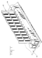
- FIGURE 1 is a perspective view of a right angle, backplane connector for electrically interconnecting a mother board to a daughter board, where the opposed housings, mounted to the mother board, may incorporate the inventive features of this invention.
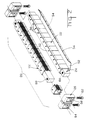
- FIGURE 2 is an exploded, perspective view of the connector housing utilizing the intermatable housing segments according to this invention.
- FIGURE 3 is an enlarged perspective view of plural housing segments, showing a pair of such housings aligned and intermated, and a third housing segment aligned but exploded therefrom.
- FIGURE 4 is a front view of the pair of aligned and intermated housing segments of Figure 3.
- FIGURE 5 is a view similar to Figure 4 but showing plural canted coiled springs arranged within the like plurality of aligned slots or channels.
- the present invention is directed to an improved housing assembly for supporting and electrically interconnecting a pair of planar electronic devices arranged at a right angle to one another.
- this invention relates to plural housing segments arranged to form a housing member for a board-to-board connector assembly.
- Figure 1 illustrates a typical connector for which the present invention may apply. Specifically, the assembly thereof includes a pair of planar electronic devices, such as a mother board 10 and a daughter board 12, and a connector housing assembly 14 for receiving and applying a normal force to the daughter board 12 received therein.
- Figures 2-5 illustrate more clearly the construction features of a modified connector housing assembly for use in the connector 20 of this invention.
- the connector 20 of this invention comprises a plurality of housing segments 22, illustrated in detail in Figures 3-5, a rigid central core member 24 for slidably receiving said housing segments 22 in aligned relationship, and end housings 26 for securing the connector 20 to an underlying planar electronic device, such as a mother board, as known in the art.
- the modular housing segments 22 illustrated in Figures 3-5 comprise a generally rectangular member consisting of four walls, where a pair of such walls, namely, bottom 30 and front face 32, are provided with plural, parallel channels or grooves 34 for receiving therein a coiled spring 36, see Figure 5.
- the connector 20 includes a series of springs 36 which fit into the grooves 34 and extend across the front face 32 of the connector 20 in contact with the surface of the daughter card 14.
- These springs shown as coil springs, may be of the canted coil variety, a reference being made to U.S. Patent No. 4,969,824 for a description of canted coil spring structures. It is contemplated that other spring means may be provided to drive contacts in a manner to be described to effect an adequate normal bearing force between contacts being interconnected.
- a typical spring 36 is oval configured, with a width of about .078 inches, a height of about .070 inches, and a wire gauge of about .006 inches.
- the mating edges 40 of the bottom face 30 and front face 32 are sawtoothed configured 42 at an angle of about 45°.
- the internal housing segments 22, i.e. those segments sawtoothed along both the outside edges 40 are identical such that the groove extension 44 on one edge will intermate or be received within the recess 46 along the side of an adjacent housing module.
- adjacent grooves 34 are oppositely angled, namely about 90° to one another for a preferred embodiment.
- Figure 5 illustrates the manner by which the springs 36 are oriented within the respective grooves 34. It will be noted that the convolutions of the springs are arranged to cross the gap 50, at an angle of about 90°, to thereby avoid the problems associated with the prior art. While an obvious solution would have been to eliminate the gaps by providing a continuous housing, the modular concept allows for the selection of different sized connector to receive a variety of PCBs. However, by accepting that flexibility, performance problems arose. It will be appreciated that with a gap width of from .005 to .010 inches, and a typical wire gauge of .006 inches, such wire can become trapped in the gap affecting the spring's performance. By arranging the springs in the manner illustrated in Figure 5, the wire trapping problem is eliminated.
- the purpose of the springs 36 is to provide a normal force to an overlying flexible film 52 on which circuit traces or pads are arranged to electrically interconnect with corresponding traces or pads on the mother board 10 and daughter board 12, as known in the art.
- Figure 2 illustrates one of the housing members as having a flexible film 52 partially wrapped about a housing member. The film 52 may be secured thereabout by overlapping the film along the top, where plural aligned holes 54 in the film are received on plural projections 56, which in turn are heat staked, in a manner known in the art, to prevent premature removal of the film.
- a pair of end housings 26 are provided to secure the connector 20 to the first of the two planar electronic devices, i.e. mother board, not shown in Figure 2.
- the end housings 26 are rectangular in configuration, with a central opening 58, to receive the rigid central core member 24 at each end thereof.
- Such core members 24 are provided with threaded openings 60 to receive threaded members 62.
- the end housings 26, along the base include threaded openings 64 which are aligned with the threaded openings 60 in the core members. In this position, threaded members 62 are passed through openings (not shown) in the mother board, then threaded into the respective openings 60,64.
- the housing members are mounted to the mother board to receive and electrically engage the daughter board between the respective housing members.
Landscapes
- Engineering & Computer Science (AREA)
- Microelectronics & Electronic Packaging (AREA)
- Coupling Device And Connection With Printed Circuit (AREA)
Applications Claiming Priority (2)
| Application Number | Priority Date | Filing Date | Title |
|---|---|---|---|
| US169453 | 1993-12-17 | ||
| US08/169,453 US5368491A (en) | 1993-12-17 | 1993-12-17 | High density electrical connector |
Publications (2)
| Publication Number | Publication Date |
|---|---|
| EP0658957A2 true EP0658957A2 (fr) | 1995-06-21 |
| EP0658957A3 EP0658957A3 (fr) | 1996-10-30 |
Family
ID=22615767
Family Applications (1)
| Application Number | Title | Priority Date | Filing Date |
|---|---|---|---|
| EP94308195A Withdrawn EP0658957A3 (fr) | 1993-12-17 | 1994-11-08 | Connecteur électrique à haute densité. |
Country Status (3)
| Country | Link |
|---|---|
| US (1) | US5368491A (fr) |
| EP (1) | EP0658957A3 (fr) |
| JP (1) | JPH07211411A (fr) |
Families Citing this family (3)
| Publication number | Priority date | Publication date | Assignee | Title |
|---|---|---|---|---|
| US5704793A (en) * | 1995-04-17 | 1998-01-06 | Teradyne, Inc. | High speed high density connector for electronic signals |
| US6000955A (en) * | 1997-12-10 | 1999-12-14 | Gabriel Technologies, Inc. | Multiple terminal edge connector |
| JP7364620B2 (ja) * | 2021-05-14 | 2023-10-18 | 矢崎総業株式会社 | コネクタ、電子制御ユニット、端子部品及び一対の端部品 |
Family Cites Families (7)
| Publication number | Priority date | Publication date | Assignee | Title |
|---|---|---|---|---|
| US4969824A (en) * | 1989-07-28 | 1990-11-13 | Amp Incorporated | Electrical connector |
| US5176530A (en) * | 1990-04-18 | 1993-01-05 | Minnesota Mining And Manufacturing Company | Miniature multiple conductor electrical connector |
| US5118299A (en) * | 1990-05-07 | 1992-06-02 | International Business Machines Corporation | Cone electrical contact |
| EP0653819A3 (fr) * | 1990-11-08 | 1996-11-27 | Whitaker Corp | Connecteur électrique de haute densité. |
| US5171154A (en) * | 1991-11-06 | 1992-12-15 | Amp Incorporated | High density backplane connector |
| US5251106A (en) * | 1992-03-06 | 1993-10-05 | Everex Systems, Inc. | Stackable enclosure for electronic devices |
| US5306171A (en) * | 1992-08-07 | 1994-04-26 | Elco Corporation | Bowtie connector with additional leaf contacts |
-
1993
- 1993-12-17 US US08/169,453 patent/US5368491A/en not_active Expired - Fee Related
-
1994
- 1994-11-08 EP EP94308195A patent/EP0658957A3/fr not_active Withdrawn
- 1994-12-16 JP JP6333949A patent/JPH07211411A/ja active Pending
Also Published As
| Publication number | Publication date |
|---|---|
| EP0658957A3 (fr) | 1996-10-30 |
| US5368491A (en) | 1994-11-29 |
| JPH07211411A (ja) | 1995-08-11 |
Similar Documents
| Publication | Publication Date | Title |
|---|---|---|
| US4331370A (en) | Connection system for printed circuit boards | |
| US3591834A (en) | Circuit board connecting means | |
| EP0130556B1 (fr) | Connecteur pour cicuits imprimés à force d'insertion nulle comprenant un système de détrompage | |
| EP0748527B1 (fr) | Connecteur de bords d'une carte a circuits imprimes assurant des connexions electriques non simultanees | |
| US4846727A (en) | Reference conductor for improving signal integrity in electrical connectors | |
| EP0757851B1 (fr) | Enveloppe conductrice pour connecteurs electriques | |
| EP0676833B1 (fr) | Connecteur de bord de carte à montage de surface | |
| US4674812A (en) | Backplane wiring for electrical printed circuit cards | |
| US8485831B2 (en) | Tall mezzanine connector | |
| EP0520283B1 (fr) | Connecteur avec structure de mise à la masse | |
| US3660803A (en) | Electrical connectors | |
| US5197887A (en) | High density circuit connector | |
| US5967831A (en) | Electrical connector assembly | |
| CA2532378A1 (fr) | Connecteur electrique a grande vitesse | |
| US6053757A (en) | Printed circuit board edge card connector having two non-redundant rows of contacts | |
| JPS6178079A (ja) | コネクタ組立体 | |
| US5531615A (en) | Coplanar computer docking apparatus | |
| US7438556B2 (en) | Electrical interconnection between multiple printed circuit boards | |
| US5788510A (en) | Socket having a staggered conductive path through multiple memory modules | |
| WO1998022994A1 (fr) | Connecteur de fond de panier a grande vitesse et haute densite | |
| EP0766854B1 (fr) | Connecteur pour cartes sim | |
| US4832619A (en) | Pin mounted support system for printed circuit cards and connectors | |
| US5368491A (en) | High density electrical connector | |
| US6551113B1 (en) | Connector for signal channel | |
| EP0373355B1 (fr) | Système de détrompage |
Legal Events
| Date | Code | Title | Description |
|---|---|---|---|
| PUAI | Public reference made under article 153(3) epc to a published international application that has entered the european phase |
Free format text: ORIGINAL CODE: 0009012 |
|
| AK | Designated contracting states |
Kind code of ref document: A2 Designated state(s): DE FR GB IT NL |
|
| PUAL | Search report despatched |
Free format text: ORIGINAL CODE: 0009013 |
|
| AK | Designated contracting states |
Kind code of ref document: A3 Designated state(s): DE FR GB IT NL |
|
| STAA | Information on the status of an ep patent application or granted ep patent |
Free format text: STATUS: THE APPLICATION IS DEEMED TO BE WITHDRAWN |
|
| 18D | Application deemed to be withdrawn |
Effective date: 19970502 |