EP0660395A2 - Contact auto-aligné avec un décalage de zéro pour la grille - Google Patents
Contact auto-aligné avec un décalage de zéro pour la grille Download PDFInfo
- Publication number
- EP0660395A2 EP0660395A2 EP94308578A EP94308578A EP0660395A2 EP 0660395 A2 EP0660395 A2 EP 0660395A2 EP 94308578 A EP94308578 A EP 94308578A EP 94308578 A EP94308578 A EP 94308578A EP 0660395 A2 EP0660395 A2 EP 0660395A2
- Authority
- EP
- European Patent Office
- Prior art keywords
- dielectric
- conductor layer
- layer
- locations
- thin
- Prior art date
- Legal status (The legal status is an assumption and is not a legal conclusion. Google has not performed a legal analysis and makes no representation as to the accuracy of the status listed.)
- Withdrawn
Links
Images


Classifications
-
- H—ELECTRICITY
- H10—SEMICONDUCTOR DEVICES; ELECTRIC SOLID-STATE DEVICES NOT OTHERWISE PROVIDED FOR
- H10W—GENERIC PACKAGES, INTERCONNECTIONS, CONNECTORS OR OTHER CONSTRUCTIONAL DETAILS OF DEVICES COVERED BY CLASS H10
- H10W20/00—Interconnections in chips, wafers or substrates
- H10W20/01—Manufacture or treatment
- H10W20/031—Manufacture or treatment of conductive parts of the interconnections
- H10W20/069—Manufacture or treatment of conductive parts of the interconnections by forming self-aligned vias or self-aligned contact plugs
-
- H—ELECTRICITY
- H10—SEMICONDUCTOR DEVICES; ELECTRIC SOLID-STATE DEVICES NOT OTHERWISE PROVIDED FOR
- H10D—INORGANIC ELECTRIC SEMICONDUCTOR DEVICES
- H10D30/00—Field-effect transistors [FET]
- H10D30/01—Manufacture or treatment
- H10D30/021—Manufacture or treatment of FETs having insulated gates [IGFET]
- H10D30/0223—Manufacture or treatment of FETs having insulated gates [IGFET] having source and drain regions or source and drain extensions self-aligned to sides of the gate
- H10D30/0227—Manufacture or treatment of FETs having insulated gates [IGFET] having source and drain regions or source and drain extensions self-aligned to sides of the gate having both lightly-doped source and drain extensions and source and drain regions self-aligned to the sides of the gate, e.g. lightly-doped drain [LDD] MOSFET or double-diffused drain [DDD] MOSFET
-
- H—ELECTRICITY
- H10—SEMICONDUCTOR DEVICES; ELECTRIC SOLID-STATE DEVICES NOT OTHERWISE PROVIDED FOR
- H10W—GENERIC PACKAGES, INTERCONNECTIONS, CONNECTORS OR OTHER CONSTRUCTIONAL DETAILS OF DEVICES COVERED BY CLASS H10
- H10W20/00—Interconnections in chips, wafers or substrates
- H10W20/01—Manufacture or treatment
Definitions
- the present invention relates to integrated circuit fabrication methods and structures, and particularly to integrated circuits with minimum linewidths below one-half micron.
- the disclosed innovations are particularly useful for the sub-half-micron regime, and are thus particularly relevant to product generations such as 16M SRAMs and 64M DRAMs.
- a thick oxide has been deposited on top of the polycide prior to pattern and etch. Although this buys more margin, it still does not resolve the problem. 1Where the material underlying a photoresist layer is reflective and nonplanar, light may be reflected laterally from a more-illuminated location to a less-illuminated location, degrading the accuracy of patterning.
- Another method uses a second poly as the "landing pads" for bitline contacts in the matrix. In this way, the wordlines are protected thereby allowing for zero contact-to-gate spacing.
- the drawback is that this method cannot be used in the periphery due to contact resistance problems which result in slower operation of the device.
- Another method uses a silicon nitride deposition on top of the polycide prior to pattern and etch.
- a silicon nitride deposition on top of the polycide prior to pattern and etch.
- This will reduce the possibility of the contact touching the top of the polycide; however, it can still make contact along the sidewall due to the removal of the oxide spacer. Additionally, this does not address the problem of overetching the field oxide during the spacer etch.
- Still another proposed method uses an Al2O3 etch-stop layer to achieve a zero-margin contact process.
- an Al2O3 etch-stop layer to achieve a zero-margin contact process.
- the disclosed inventions describe new methods of forming self-aligned contact utilizing Si3N4 (or other dielectric film with lower reflectivity than WSi x film and good etch selectivity to oxide film; e.g . oxynitride, metallic oxides, etc.).
- Si3N4 film can be used as follows:
- the disclosed innovative techniques are used to simultaneously form contacts to multiple levels of poly/polycide, as well as to active areas (both for multiple poly interconnecting and metal interconnects), with zero contact-to-poly spacing. This is a significant advantage. Furthermore, this technique can be applied both in the memory array and in the circuit periphery without any degradation in circuit performance.
- a polysilicon reoxidation step is performed, after the gate etch, to ensure that a pad oxide is present under the nitride spacers which are then formed on the sidewalls of the gate. This helps to avoid accumulated charge due to trapping of hot carriers.
- An integrated circuit fabrication method comprising the steps of: providing a substrate which includes exposed surface portions of substantially monolithic semiconductor material separated by regions of field dielectric; forming a gate dielectric on said surface portions; forming a first thin-film conductor layer over said gate dielectric and said field dielectric; forming a first thin-film dielectric layer over said first conductor layer; selectively removing said first dielectric layer from locations where contact to said first conductor layer will be formed over said field dielectric; anisotropically etching said first conductor layer, together with said first dielectric layer thereover, to leave said conductor layer in a pattern which provides transistor gates in desired locations, and also exposes locations where contact will be formed to said surface portions of said semiconductor material; performing oxidation, to grow an oxide layer on exposed portions of said conductor layer and said surface portions; depositing a second layer of dielectric material overall, and anisotropically etching said second layer to leave sidewall spacers adjacent to edges of said conductor layer;
- An integrated circuit fabrication method comprising the steps of: providing a substrate which includes exposed surface portions of substantially monolithic semiconductor material separated by regions of field dielectric; forming a gate dielectric on said surface portions; forming a first thin-film conductor layer over said gate dielectric and said field dielectric; forming a first thin-film dielectric layer over said first conductor layer; selectively removing said first dielectric layer from locations where contact to said first conductor layer will be formed over said field dielectric; anisotropically etching said first conductor layer, together with said first dielectric layer thereover, to leave said conductor layer in a pattern which provides transistor gates in desired locations, and also exposes locations where contact will be formed to said surface portions of said semiconductor material; performing oxidation, to grow an oxide layer on exposed portions of said conductor layer and said surface portions; depositing a second layer of dielectric material overall, and anisotropically etching said second layer to leave sidewall spacers adjacent to edges of said conductor layer; deposit
- An integrated circuit fabrication method comprising the steps of: providing a substrate which includes exposed surface portions of substantially monolithic semiconductor material separated by regions of field dielectric; forming a gate dielectric on said surface portions; forming a first thin-film conductor layer over said gate dielectric and said field dielectric; forming a first thin-film dielectric layer over said first conductor layer; selectively removing said first dielectric layer from locations where contact to said first conductor layer will be formed over said field dielectric; anisotropically etching said first conductor layer, together with said first dielectric layer thereover, to leave said conductor layer in a pattern which provides transistor gates in desired locations, and also exposes locations where contact will be formed to said surface portions of said semiconductor material; performing oxidation, to grow an oxide layer on exposed portions of said conductor layer and said surface portions; depositing a second layer of dielectric material overall, and anisotropically etching said second layer to leave sidewall spacers adjacent to edges of said conductor layer; deposit
- An integrated circuit comprising: a body of monocrystalline semiconductor material, having active areas therein separated by field dielectric regions of a first dielectric material; a first patterned thin-film conductor layer , capacitively coupled to said semiconductor material in multiple transistor channel locations in said active areas, and also running across portions of said field dielectric regions; an interlevel dielectric material overlying said first thin-film conductor layer, and having contact holes therein; a second patterned thin-film conductor layer overlying said interlevel dielectric material, and extending down through said contact holes to make contact to said first conductor layer in selected locations, and also to said active areas in selected locations; wherein a layer of a second dielectric material, which is different from said first dielectric material and from said interlevel dielectric material, overlies said first thin-film conductor, beneath said interlevel dielectric; and wherein sidewall spacers of said second dielectric material abut sidewalls of said first conductor layer at said selected locations.
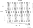
- Figure 1 shows a simple example of an integrated circuit structure.
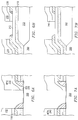
- Figures 2A-7A show sequential process steps along section A-A of Figure 1
- corresponding Figures 2B-7B show the same sequence of process steps along section B-B of Figure 1.
- Figure 1 shows a simple example of an integrated circuit structure.
- this is a simplified example of a device structure, which includes features in common with many high-density structures, including not only memory cells, large output transistors, etc.
- transistor locations 102 i.e . locations where poly crosses over Active
- first-poly-contact location 104 where contact is made to poly over field oxide occurs along section line B-B.
- first-poly-contact locations are NOT related to the "first contacts" or direct contacts which were sometimes used, in the 1970s and 1980s, to form contacts directly from first poly to active.
- Figures 2A, 3A, 4A, etc. show sequential process steps at transistor gate sidewall locations 102 (along section A-A), and corresponding Figures 2B, 3B, 4B, etc ., show the same sequence of process steps at first-poly-contact location 104 (along section B-B).
- the anti-reflective layer 214 and the sidewall filaments 220 can alternatively be formed of materials other than silicon nitride.
- oxynitrides can be used, or other dielectric materials which have lower reflectivity than a silicide and good etch selectivity to oxide film; i.e . oxynitride, metallic oxides, etc.
- anti-reflective layer 214 and the sidewall spacers 220 do not necessarily have to be composed of identical materials (although both should be materials which have some ability to withstand an oxide etch).
Landscapes
- Internal Circuitry In Semiconductor Integrated Circuit Devices (AREA)
- Metal-Oxide And Bipolar Metal-Oxide Semiconductor Integrated Circuits (AREA)
- Insulated Gate Type Field-Effect Transistor (AREA)
- Drying Of Semiconductors (AREA)
Applications Claiming Priority (2)
| Application Number | Priority Date | Filing Date | Title |
|---|---|---|---|
| US08/169,587 US5439846A (en) | 1993-12-17 | 1993-12-17 | Self-aligned method for forming contact with zero offset to gate |
| US169587 | 1993-12-17 |
Publications (2)
| Publication Number | Publication Date |
|---|---|
| EP0660395A2 true EP0660395A2 (fr) | 1995-06-28 |
| EP0660395A3 EP0660395A3 (fr) | 1997-05-14 |
Family
ID=22616325
Family Applications (1)
| Application Number | Title | Priority Date | Filing Date |
|---|---|---|---|
| EP94308578A Withdrawn EP0660395A3 (fr) | 1993-12-17 | 1994-11-21 | Contact auto-aligné avec un décalage de zéro pour la grille. |
Country Status (3)
| Country | Link |
|---|---|
| US (2) | US5439846A (fr) |
| EP (1) | EP0660395A3 (fr) |
| JP (1) | JPH07221194A (fr) |
Cited By (4)
| Publication number | Priority date | Publication date | Assignee | Title |
|---|---|---|---|---|
| WO1997036321A1 (fr) * | 1996-03-27 | 1997-10-02 | Advanced Micro Devices, Inc. | Procede de dopage separe des zones polygrille et drain-source |
| EP0809281A3 (fr) * | 1996-05-20 | 1997-12-10 | Texas Instruments Incorporated | Améliorations aux ou relatives aux dispositifs semi-conducteurs |
| EP1026739A1 (fr) * | 1999-02-08 | 2000-08-09 | Chartered Semiconductor Manufacturing Pte Ltd. | Procédé selectif salicide par reformation des parois latérales d'espacement de nitrure |
| DE19929684B4 (de) * | 1998-06-29 | 2009-12-31 | Samsung Electronics Co., Ltd., Suwon | Verfahren für die Ausbildung eines von einem Schmalkanaleffekt freien Transistors durch Verwendung einer in die Flachgrabenisolation eingebetteten, leitenden Abschirmung |
Families Citing this family (24)
| Publication number | Priority date | Publication date | Assignee | Title |
|---|---|---|---|---|
| US5880036A (en) * | 1992-06-15 | 1999-03-09 | Micron Technology, Inc. | Method for enhancing oxide to nitride selectivity through the use of independent heat control |
| US6284584B1 (en) | 1993-12-17 | 2001-09-04 | Stmicroelectronics, Inc. | Method of masking for periphery salicidation of active regions |
| US6057604A (en) * | 1993-12-17 | 2000-05-02 | Stmicroelectronics, Inc. | Integrated circuit contact structure having gate electrode protection for self-aligned contacts with zero enclosure |
| US6107194A (en) * | 1993-12-17 | 2000-08-22 | Stmicroelectronics, Inc. | Method of fabricating an integrated circuit |
| JPH09205185A (ja) | 1996-01-26 | 1997-08-05 | Mitsubishi Electric Corp | 半導体装置および半導体装置の製造方法 |
| US5846873A (en) * | 1996-02-02 | 1998-12-08 | Micron Technology, Inc. | Method of creating ultra-small nibble structures during mosfet fabrication |
| US5739066A (en) | 1996-09-17 | 1998-04-14 | Micron Technology, Inc. | Semiconductor processing methods of forming a conductive gate and line |
| US20020137890A1 (en) * | 1997-03-31 | 2002-09-26 | Genentech, Inc. | Secreted and transmembrane polypeptides and nucleic acids encoding the same |
| US6258671B1 (en) * | 1997-05-13 | 2001-07-10 | Micron Technology, Inc. | Methods of providing spacers over conductive line sidewalls, methods of forming sidewall spacers over etched line sidewalls, and methods of forming conductive lines |
| US6080672A (en) | 1997-08-20 | 2000-06-27 | Micron Technology, Inc. | Self-aligned contact formation for semiconductor devices |
| JP3156765B2 (ja) * | 1997-08-29 | 2001-04-16 | 日本電気株式会社 | 半導体装置、および半導体装置の製造方法 |
| JP3061017B2 (ja) * | 1997-10-31 | 2000-07-10 | 日本電気株式会社 | 集積回路装置の実装構造およびその実装方法 |
| US6262445B1 (en) | 1998-03-30 | 2001-07-17 | Texas Instruments Incorporated | SiC sidewall process |
| US6165880A (en) * | 1998-06-15 | 2000-12-26 | Taiwan Semiconductor Manufacturing Company | Double spacer technology for making self-aligned contacts (SAC) on semiconductor integrated circuits |
| US6143611A (en) * | 1998-07-30 | 2000-11-07 | Micron Technology, Inc. | Semiconductor processing methods, methods of forming electronic components, and transistors |
| US6806154B1 (en) | 1998-10-08 | 2004-10-19 | Integrated Device Technology, Inc. | Method for forming a salicided MOSFET structure with tunable oxynitride spacer |
| US6133096A (en) * | 1998-12-10 | 2000-10-17 | Su; Hung-Der | Process for simultaneously fabricating a stack gate flash memory cell and salicided periphereral devices |
| US6248638B1 (en) * | 1998-12-18 | 2001-06-19 | Texas Instruments Incorporated | Enhancements to polysilicon gate |
| US6316321B1 (en) * | 1999-05-19 | 2001-11-13 | United Microelectronics Corp. | Method for forming MOSFET |
| KR100426811B1 (ko) * | 2001-07-12 | 2004-04-08 | 삼성전자주식회사 | 셀프얼라인 콘택을 갖는 반도체 소자 및 그의 제조방법 |
| KR100444492B1 (ko) * | 2002-05-16 | 2004-08-16 | 주식회사 하이닉스반도체 | 반도체소자의 제조 방법 |
| EP1403909A1 (fr) * | 2002-09-30 | 2004-03-31 | STMicroelectronics S.r.l. | Procédé de fabrication d'une résistance intégrée avec une protection contre la silicidation |
| US7981745B2 (en) * | 2007-08-30 | 2011-07-19 | Spansion Llc | Sacrificial nitride and gate replacement |
| FR3107988B1 (fr) * | 2020-03-05 | 2023-11-10 | St Microelectronics Tours Sas | Formation d'un thyristor, triac ou diode de suppression de tensions transitoires |
Family Cites Families (67)
| Publication number | Priority date | Publication date | Assignee | Title |
|---|---|---|---|---|
| DE185787C (fr) * | ||||
| JPS54107270A (en) * | 1978-02-10 | 1979-08-22 | Nec Corp | Semiconductor device and its production |
| GB2024505B (en) * | 1978-05-26 | 1983-03-23 | Rockwell International Corp | Manufacture of integrated circuits |
| US4253907A (en) * | 1979-03-28 | 1981-03-03 | Western Electric Company, Inc. | Anisotropic plasma etching |
| JPS56164578A (en) * | 1980-05-21 | 1981-12-17 | Oki Electric Ind Co Ltd | Manufacture of mos type semiconductor device |
| US4354896A (en) * | 1980-08-05 | 1982-10-19 | Texas Instruments Incorporated | Formation of submicron substrate element |
| US4333964A (en) * | 1980-09-15 | 1982-06-08 | General Electric Company | Method of making integrated circuits |
| JPS59106172A (ja) * | 1982-12-07 | 1984-06-19 | インタ−ナシヨナル ビジネス マシ−ンズ コ−ポレ−シヨン | 電界効果トランジスタの製造方法 |
| JPS59159544A (ja) * | 1983-03-03 | 1984-09-10 | Nec Corp | 半導体装置およびその製造方法 |
| JPS6058635A (ja) * | 1983-09-12 | 1985-04-04 | Toshiba Corp | 半導体装置の製造方法 |
| JPS60246675A (ja) * | 1984-05-22 | 1985-12-06 | Seiko Instr & Electronics Ltd | 半導体装置の製造方法 |
| US4543271A (en) * | 1984-07-02 | 1985-09-24 | Hughes Aircraft Company | Silicon oxynitride material and photochemical process for forming same |
| JPS6116571A (ja) * | 1984-07-03 | 1986-01-24 | Ricoh Co Ltd | 半導体装置の製造方法 |
| JPS6126240A (ja) * | 1984-07-17 | 1986-02-05 | Hitachi Ltd | 絶縁分離方法 |
| US4656732A (en) * | 1984-09-26 | 1987-04-14 | Texas Instruments Incorporated | Integrated circuit fabrication process |
| US4654112A (en) * | 1984-09-26 | 1987-03-31 | Texas Instruments Incorporated | Oxide etch |
| US4686000A (en) * | 1985-04-02 | 1987-08-11 | Heath Barbara A | Self-aligned contact process |
| JPS61232646A (ja) * | 1985-04-09 | 1986-10-16 | Nec Corp | 樹脂封止型半導体集積回路装置 |
| US4657628A (en) * | 1985-05-01 | 1987-04-14 | Texas Instruments Incorporated | Process for patterning local interconnects |
| US4715109A (en) * | 1985-06-12 | 1987-12-29 | Texas Instruments Incorporated | Method of forming a high density vertical stud titanium silicide for reachup contact applications |
| US4755476A (en) * | 1985-12-17 | 1988-07-05 | Siemens Aktiengesellschaft | Process for the production of self-adjusted bipolar transistor structures having a reduced extrinsic base resistance |
| JPS62150826A (ja) * | 1985-12-25 | 1987-07-04 | Toshiba Corp | 半導体装置の製造方法 |
| DE3684298D1 (de) * | 1986-01-09 | 1992-04-16 | Ibm | Verfahren zur herstellung eines kontakts unter verwendung der erweichung zweier glasschichten. |
| US4707218A (en) * | 1986-10-28 | 1987-11-17 | International Business Machines Corporation | Lithographic image size reduction |
| US4801350A (en) * | 1986-12-29 | 1989-01-31 | Motorola, Inc. | Method for obtaining submicron features from optical lithography technology |
| US5256895A (en) * | 1987-02-24 | 1993-10-26 | Sgs-Thomson Microelectronics, Inc. | Pad oxide protect sealed interface isolation |
| US4721548A (en) * | 1987-05-13 | 1988-01-26 | Intel Corporation | Semiconductor planarization process |
| JPS63293946A (ja) * | 1987-05-27 | 1988-11-30 | Matsushita Electric Ind Co Ltd | 半導体装置の製造方法 |
| US4988423A (en) * | 1987-06-19 | 1991-01-29 | Matsushita Electric Industrial Co., Ltd. | Method for fabricating interconnection structure |
| GB2207281B (en) * | 1987-07-24 | 1992-02-05 | Plessey Co Plc | A method of providing refilled trenches |
| US4801560A (en) * | 1987-10-02 | 1989-01-31 | Motorola Inc. | Semiconductor processing utilizing carbon containing thick film spin-on glass |
| FR2625839B1 (fr) * | 1988-01-13 | 1991-04-26 | Sgs Thomson Microelectronics | Procede de passivation d'un circuit integre |
| US4962414A (en) * | 1988-02-11 | 1990-10-09 | Sgs-Thomson Microelectronics, Inc. | Method for forming a contact VIA |
| US4894351A (en) * | 1988-02-16 | 1990-01-16 | Sprague Electric Company | Method for making a silicon IC with planar double layer metal conductors system |
| US4912061A (en) * | 1988-04-04 | 1990-03-27 | Digital Equipment Corporation | Method of forming a salicided self-aligned metal oxide semiconductor device using a disposable silicon nitride spacer |
| US4818335A (en) * | 1988-05-13 | 1989-04-04 | The United States Of America As Represented By The Director Of The National Security Agency | Tapered wet etching of contacts using a trilayer silox structure |
| US4986878A (en) * | 1988-07-19 | 1991-01-22 | Cypress Semiconductor Corp. | Process for improved planarization of the passivation layers for semiconductor devices |
| US5244841A (en) * | 1988-11-10 | 1993-09-14 | Applied Materials, Inc. | Method for planarizing an integrated circuit structure using low melting inorganic material and flowing while depositing |
| JPH02192724A (ja) * | 1989-01-20 | 1990-07-30 | Mitsubishi Electric Corp | 半導体装置およびその製造方法 |
| KR920004541B1 (ko) * | 1989-05-30 | 1992-06-08 | 현대전자산업 주식회사 | 반도체 소자에서 식각베리어층을 사용한 콘택홀 형성방법 |
| JPH03133131A (ja) * | 1989-10-18 | 1991-06-06 | Mitsubishi Electric Corp | 半導体装置 |
| US5200808A (en) * | 1989-11-29 | 1993-04-06 | Mitsubishi Denki Kabushiki Kaisha | Semiconductor device having smooth contact holes formed through multi-layer insulators of different etching speeds |
| JP2518435B2 (ja) * | 1990-01-29 | 1996-07-24 | ヤマハ株式会社 | 多層配線形成法 |
| CA2009518C (fr) * | 1990-02-07 | 2000-10-17 | Luc Ouellet | Methode de fabrication de dispositifs a semiconducteur par depot d'une couche de spin sur verre |
| US5181096A (en) * | 1990-04-12 | 1993-01-19 | Actel Corporation | Electrically programmable antifuse incorporating dielectric and amorphous silicon interlayer |
| US5003062A (en) * | 1990-04-19 | 1991-03-26 | Taiwan Semiconductor Manufacturing Co. | Semiconductor planarization process for submicron devices |
| JP2545154B2 (ja) * | 1990-06-04 | 1996-10-16 | 松下電器産業株式会社 | コンタクト構造の形成方法 |
| US5061646A (en) * | 1990-06-29 | 1991-10-29 | Motorola, Inc. | Method for forming a self-aligned bipolar transistor |
| US5166088A (en) * | 1990-07-03 | 1992-11-24 | Sharp Kabushiki Kaisha | Method of manufacturing semiconductor device contact vias in layers comprising silicon nitride and glass |
| KR940009352B1 (ko) * | 1990-07-09 | 1994-10-07 | 가부시끼가이샤 도시바 | 반도체 소자 |
| JP3128811B2 (ja) * | 1990-08-07 | 2001-01-29 | セイコーエプソン株式会社 | 半導体装置の製造方法 |
| JPH0492453A (ja) * | 1990-08-08 | 1992-03-25 | Seiko Epson Corp | 半導体装置 |
| US5158910A (en) * | 1990-08-13 | 1992-10-27 | Motorola Inc. | Process for forming a contact structure |
| US5214305A (en) * | 1990-08-28 | 1993-05-25 | United Microelectronics Corporation | Polycide gate MOSFET for integrated circuits |
| US5117273A (en) * | 1990-11-16 | 1992-05-26 | Sgs-Thomson Microelectronics, Inc. | Contact for integrated circuits |
| IT1243919B (it) * | 1990-11-20 | 1994-06-28 | Cons Ric Microelettronica | Procedimento per l'ottenimento di solchi submicrometrici planarizzati in circuiti integrati realizzati con tecnologia ulsi |
| JP2848694B2 (ja) * | 1990-11-28 | 1999-01-20 | 株式会社東芝 | 半導体装置 |
| US5380553A (en) * | 1990-12-24 | 1995-01-10 | Dow Corning Corporation | Reverse direction pyrolysis processing |
| EP0523856A3 (en) * | 1991-06-28 | 1993-03-17 | Sgs-Thomson Microelectronics, Inc. | Method of via formation for multilevel interconnect integrated circuits |
| US5260229A (en) * | 1991-08-30 | 1993-11-09 | Sgs-Thomson Microelectronics, Inc. | Method of forming isolated regions of oxide |
| JPH0574958A (ja) * | 1991-09-13 | 1993-03-26 | Nec Corp | 半導体装置およびその製造方法 |
| DE4132140A1 (de) * | 1991-09-26 | 1993-04-08 | Siemens Ag | Verfahren zur herstellung einer selbstjustierten kontaktlochanordnung und selbstjustierte kontaktlochanordnung |
| US5266516A (en) * | 1992-01-02 | 1993-11-30 | Chartered Semiconductor Manufacturing Pte Ltd | Method for making electrical contact through an opening of one micron or less for CMOS technology |
| US5323047A (en) * | 1992-01-31 | 1994-06-21 | Sgs-Thomson Microelectronics, Inc. | Structure formed by a method of patterning a submicron semiconductor layer |
| JPH05243223A (ja) * | 1992-02-28 | 1993-09-21 | Fujitsu Ltd | 集積回路装置の製造方法 |
| JPH05267477A (ja) * | 1992-03-19 | 1993-10-15 | Nippon Semiconductor Kk | 半導体装置 |
| US5250472A (en) * | 1992-09-03 | 1993-10-05 | Industrial Technology Research Institute | Spin-on-glass integration planarization having siloxane partial etchback and silicate processes |
-
1993
- 1993-12-17 US US08/169,587 patent/US5439846A/en not_active Expired - Lifetime
-
1994
- 1994-11-21 EP EP94308578A patent/EP0660395A3/fr not_active Withdrawn
- 1994-12-19 JP JP6314700A patent/JPH07221194A/ja active Pending
-
1996
- 1996-04-24 US US08/639,316 patent/US5793114A/en not_active Expired - Lifetime
Non-Patent Citations (3)
| Title |
|---|
| FUKASE ET AL.: "A Margin-Free Contact Process Using an A1203 Etch-Stop Layer for High-Density Devices", IEDM PROCEEDINGS 33.3, 1992 |
| SINGER: "A New Technology for Oxide Contact and Via Etch", SEMICON-DUCTOR INTERNATIONAL, August 1993 (1993-08-01), pages 36 |
| SINGER: "A New Technology for Oxide Contact and Via Etch", SEMICONDUCTOR INTERNATIONAL, August 1993 (1993-08-01), pages 36 |
Cited By (6)
| Publication number | Priority date | Publication date | Assignee | Title |
|---|---|---|---|---|
| WO1997036321A1 (fr) * | 1996-03-27 | 1997-10-02 | Advanced Micro Devices, Inc. | Procede de dopage separe des zones polygrille et drain-source |
| US6319804B1 (en) | 1996-03-27 | 2001-11-20 | Advanced Micro Devices, Inc. | Process to separate the doping of polygate and source drain regions in dual gate field effect transistors |
| EP0809281A3 (fr) * | 1996-05-20 | 1997-12-10 | Texas Instruments Incorporated | Améliorations aux ou relatives aux dispositifs semi-conducteurs |
| US5960304A (en) * | 1996-05-20 | 1999-09-28 | Texas Instruments Incorporated | Method for forming a contact to a substrate |
| DE19929684B4 (de) * | 1998-06-29 | 2009-12-31 | Samsung Electronics Co., Ltd., Suwon | Verfahren für die Ausbildung eines von einem Schmalkanaleffekt freien Transistors durch Verwendung einer in die Flachgrabenisolation eingebetteten, leitenden Abschirmung |
| EP1026739A1 (fr) * | 1999-02-08 | 2000-08-09 | Chartered Semiconductor Manufacturing Pte Ltd. | Procédé selectif salicide par reformation des parois latérales d'espacement de nitrure |
Also Published As
| Publication number | Publication date |
|---|---|
| US5439846A (en) | 1995-08-08 |
| EP0660395A3 (fr) | 1997-05-14 |
| US5793114A (en) | 1998-08-11 |
| JPH07221194A (ja) | 1995-08-18 |
Similar Documents
| Publication | Publication Date | Title |
|---|---|---|
| US5439846A (en) | Self-aligned method for forming contact with zero offset to gate | |
| US5744395A (en) | Low resistance, self-aligned, titanium silicide structures, using a single rapid thermal anneal procedure | |
| EP0466016B1 (fr) | Capacité métal/siliciure pour grille en polysilicium | |
| US5208472A (en) | Double spacer salicide MOS device and method | |
| US4470189A (en) | Process for making polycide structures | |
| US6388294B1 (en) | Integrated circuit using damascene gate structure | |
| US5637903A (en) | Depleted gate transistor for high voltage operation | |
| US5783479A (en) | Structure and method for manufacturing improved FETs having T-shaped gates | |
| US5742095A (en) | Method of fabricating planar regions in an integrated circuit | |
| US4453306A (en) | Fabrication of FETs | |
| US6200834B1 (en) | Process for fabricating two different gate dielectric thicknesses using a polysilicon mask and chemical mechanical polishing (CMP) planarization | |
| EP0517368B1 (fr) | Interconnexion locale pour circuits intégrés | |
| US6033962A (en) | Method of fabricating sidewall spacers for a self-aligned contact hole | |
| US6093590A (en) | Method of fabricating transistor having a metal gate and a gate dielectric layer with a high dielectric constant | |
| US5990524A (en) | Silicon oxime spacer for preventing over-etching during local interconnect formation | |
| US6010955A (en) | Electrical connection forming process for semiconductor devices | |
| US4933297A (en) | Method for etching windows having different depths | |
| US5710078A (en) | Method to improve the contact resistance of bit line metal structures to underlying polycide structures | |
| US5001082A (en) | Self-aligned salicide process for forming semiconductor devices and devices formed thereby | |
| US5504039A (en) | Method for making a self-aligned oxide gate cap | |
| EP0778614A2 (fr) | Procédé de fabrication de condensateurs intégrés | |
| EP0445756B1 (fr) | Transitor MOS à haute tension et procédé de fabrication et dispositif à semi-conducteur avec un transistor MOS à haute tension et procédé de fabrication | |
| EP0660392A1 (fr) | Méthode et structure du diélectrique intercouche pour un meilleur recouvrement métallique de marche | |
| US6187644B1 (en) | Method of removing oxynitride by forming an offset spacer | |
| US6159806A (en) | Method for increasing the effective spacer width |
Legal Events
| Date | Code | Title | Description |
|---|---|---|---|
| PUAI | Public reference made under article 153(3) epc to a published international application that has entered the european phase |
Free format text: ORIGINAL CODE: 0009012 |
|
| AK | Designated contracting states |
Kind code of ref document: A2 Designated state(s): DE FR GB IT |
|
| PUAL | Search report despatched |
Free format text: ORIGINAL CODE: 0009013 |
|
| RHK1 | Main classification (correction) |
Ipc: H01L 21/768 |
|
| AK | Designated contracting states |
Kind code of ref document: A3 Designated state(s): DE FR GB IT |
|
| 17P | Request for examination filed |
Effective date: 19971110 |
|
| STAA | Information on the status of an ep patent application or granted ep patent |
Free format text: STATUS: THE APPLICATION HAS BEEN WITHDRAWN |
|
| 18W | Application withdrawn |
Withdrawal date: 19981014 |