EP0660410A2 - Améliorations concernant multi-slot input/outputs - Google Patents
Améliorations concernant multi-slot input/outputs Download PDFInfo
- Publication number
- EP0660410A2 EP0660410A2 EP94308276A EP94308276A EP0660410A2 EP 0660410 A2 EP0660410 A2 EP 0660410A2 EP 94308276 A EP94308276 A EP 94308276A EP 94308276 A EP94308276 A EP 94308276A EP 0660410 A2 EP0660410 A2 EP 0660410A2
- Authority
- EP
- European Patent Office
- Prior art keywords
- input
- output
- pad
- width
- buffer
- Prior art date
- Legal status (The legal status is an assumption and is not a legal conclusion. Google has not performed a legal analysis and makes no representation as to the accuracy of the status listed.)
- Granted
Links
- 239000000872 buffer Substances 0.000 claims abstract description 20
- 230000002093 peripheral effect Effects 0.000 claims abstract description 3
- 230000000295 complement effect Effects 0.000 claims description 2
- 229910052710 silicon Inorganic materials 0.000 abstract description 6
- 239000010703 silicon Substances 0.000 abstract description 6
- XUIMIQQOPSSXEZ-UHFFFAOYSA-N Silicon Chemical compound [Si] XUIMIQQOPSSXEZ-UHFFFAOYSA-N 0.000 description 5
- 230000000694 effects Effects 0.000 description 1
- 239000002184 metal Substances 0.000 description 1
- 238000000034 method Methods 0.000 description 1
- XUIMIQQOPSSXEZ-IGMARMGPSA-N silicon-28 atom Chemical compound [28Si] XUIMIQQOPSSXEZ-IGMARMGPSA-N 0.000 description 1
Images

Classifications
-
- H—ELECTRICITY
- H10—SEMICONDUCTOR DEVICES; ELECTRIC SOLID-STATE DEVICES NOT OTHERWISE PROVIDED FOR
- H10D—INORGANIC ELECTRIC SEMICONDUCTOR DEVICES
- H10D84/00—Integrated devices formed in or on semiconductor substrates that comprise only semiconducting layers, e.g. on Si wafers or on GaAs-on-Si wafers
- H10D84/90—Masterslice integrated circuits
- H10D84/998—Input and output buffer/driver structures
Definitions
- the proposed invention relates to Input/Output (I/O) structures enabling significant savings in silicon chip area.
- the proposed structures are particularly suitable for high speed differential input/output interfaces such as those used in ATM/SDH switching elements.
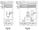
- I/O structures in differential and single ended configuration are shown in Figure 1(a) and 1(b) respectively. These consist of an I/O buffer cell which contains the input or output or input/output (in the bi-directional case) circuits to provide the desired functionality.
- power/ground busses are routed over the I/O buffer cells to feed power to the I/Os and to the core.
- global signals such as a clock and a bias reference voltage are also routed over the I/O cells.
- the pad cell is made up of a bonding pad and can also include an ESD rotection circuit.
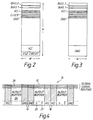
- the height (H) and the width (W) of the I/O typically depends upon one or more factors.
- One such factor is the number of interface pins required for the chip. The larger the pin count is, the narrrower the I/O has to be to maximise the pin count.
- the width of the power busses is also a factor which effects the overall height and width of the I/O.
- the width of the power busses is governed by the core and I/O current requirements and the metal electromigration capability of the process technology.
- both the circuit requirements for I/O functionality and ESD functionality and the global signal routing also contribute to the overall width and/or the height of the I/O.
- the number of interface pins and the minimum width of the I/O have greater influence on the I/O width, whilst the other factors have greater influence on the height.
- the VCC and GND pads shown in Figure 2 and 3 respectively which are needed to feed the current in and out of the chip normally use one I/O slot (i.e. one width of the I/O).
- I/O slot i.e. one width of the I/O.
- One object of the present invention is to provide an I/O structure which overcomes at least some of the disadvantages of present structures.
- an I/O structure for a device comprising at least one input/output pad; a power supply pad and input/output buffer, wherein the I/O buffer extends in a peripheral direction to a great extent that it extends inwardly, with respect to the device.
- the at least one input/output pad comprises a differential pair of signal pads, which are respectively input/output and complementary input/output; and the power supply comprises a ground pad and a supply voltage pad.
- the width of the input/output buffer is juxaposed along the width of the at least one input/output pad and at least some of the width of the power supply pad.
- One of the advantages of this is that there is a saving in the amount of silicon used for the I/O structure.
- the I/O structure of the present invention has improved performance for high speed and high differential inputs and outputs.
- the structure 10 comprises a core 12 and a plurality of pads 14 around the edge of the layout.
- the pads include ground pads 16, Vcc pads 18 and signal pads 20, 22.
- an input/output buffer 24 Associated with each pair of signal pads is an input/output buffer 24.
- the buffer is associated only with the signal pads and is juxaposed thereto along the width of the pads.
- a global signal routing channel (26) is also included to carry Vcc busses, Ground busses, bias lines (if required), etc. Since the buffer is not required for the Vcc and GND pads there is a large area of silicon 28 (shown shaded in Figure 4) which is wasted. This area 28 is sacrificed for geometrical compatibility.
- the proposed invention makes use of this shaded area by altering the aspect ratio (ratio of width to height) of the I/O buffers whilst maintaining the power feed capabilities of the structure.
- Increasing the differential I/O buffer width from two slot equivalent to approximately 4 slots will halve the I/O buffer height which in turn reduces the I/O height.
- the I/O height can be reduced from 450um to 250um.
- the overall height of the I/O structure is reduced but the area of the buffer is maintained.
- the buffer 24 extends along the width of the Vcc (18), Ground (16) and signal pads (20, 22).
- VCC/GND busses need not be as wide as used in the conventional designs which in turn helps reduce the I/O height.
- the proposed I/O layout scheme is particularly useful for high speed designs requiring high differential inputs and outputs.
- the concept can also be extended to other applications where high speed interface is limited to a few sides of the chip. Even for single ended I/Os operating at speeds in excess of 100 Mhz, a large number of power/ground pins are required to minimise the simultaneous switching noise.
- the proposed invention can be utilised to widen the I/O buffer layout.
- the I/O structure can be used on any device which requires an I/O structure.
Landscapes
- Semiconductor Integrated Circuits (AREA)
- Design And Manufacture Of Integrated Circuits (AREA)
Applications Claiming Priority (2)
| Application Number | Priority Date | Filing Date | Title |
|---|---|---|---|
| GB939323144A GB9323144D0 (en) | 1993-11-10 | 1993-11-10 | Multi-slot i/os |
| GB9323144 | 1993-11-10 |
Publications (3)
| Publication Number | Publication Date |
|---|---|
| EP0660410A2 true EP0660410A2 (fr) | 1995-06-28 |
| EP0660410A3 EP0660410A3 (fr) | 1995-08-16 |
| EP0660410B1 EP0660410B1 (fr) | 2002-05-02 |
Family
ID=10744928
Family Applications (1)
| Application Number | Title | Priority Date | Filing Date |
|---|---|---|---|
| EP94308276A Expired - Lifetime EP0660410B1 (fr) | 1993-11-10 | 1994-11-10 | Améliorations concernant multi-slot input/outputs |
Country Status (3)
| Country | Link |
|---|---|
| EP (1) | EP0660410B1 (fr) |
| DE (1) | DE69430518T2 (fr) |
| GB (1) | GB9323144D0 (fr) |
Cited By (5)
| Publication number | Priority date | Publication date | Assignee | Title |
|---|---|---|---|---|
| EP1205974A3 (fr) * | 2000-11-10 | 2003-06-25 | Seiko Epson Corporation | Procédé de placement de cellules E/S et dispositif semiconducteur |
| EP1321984A3 (fr) * | 2001-08-24 | 2004-01-14 | STMicroelectronics Limited | Système de circuit d'entrée/sortie dans un circuit intégré à semi-conducteur |
| EP1130650A3 (fr) * | 2000-01-11 | 2006-06-28 | Texas Instruments Incorporated | Architecture d'entrées/sorties pour circuits intégrés |
| WO2011023806A1 (fr) * | 2009-08-28 | 2011-03-03 | Austriamicrosystems Ag | Corps semi-conducteur comprenant une cellule de connexion |
| DE102009061167B3 (de) * | 2009-08-28 | 2015-03-05 | Austriamicrosystems Ag | Halbleiterkörper mit einer Anschlusszelle |
Family Cites Families (3)
| Publication number | Priority date | Publication date | Assignee | Title |
|---|---|---|---|---|
| JPS58190036A (ja) * | 1982-04-23 | 1983-11-05 | Fujitsu Ltd | ゲ−ト・アレイ大規模集積回路装置 |
| JP2710953B2 (ja) * | 1988-06-29 | 1998-02-10 | 株式会社日立製作所 | 半導体装置 |
| JPH02152254A (ja) * | 1988-12-02 | 1990-06-12 | Mitsubishi Electric Corp | 半導体集積回路装置 |
-
1993
- 1993-11-10 GB GB939323144A patent/GB9323144D0/en active Pending
-
1994
- 1994-11-10 EP EP94308276A patent/EP0660410B1/fr not_active Expired - Lifetime
- 1994-11-10 DE DE69430518T patent/DE69430518T2/de not_active Expired - Lifetime
Cited By (7)
| Publication number | Priority date | Publication date | Assignee | Title |
|---|---|---|---|---|
| EP1130650A3 (fr) * | 2000-01-11 | 2006-06-28 | Texas Instruments Incorporated | Architecture d'entrées/sorties pour circuits intégrés |
| EP1205974A3 (fr) * | 2000-11-10 | 2003-06-25 | Seiko Epson Corporation | Procédé de placement de cellules E/S et dispositif semiconducteur |
| US6721933B2 (en) | 2000-11-10 | 2004-04-13 | Seiko Epson Corporation | Input/output cell placement method and semiconductor device |
| EP1321984A3 (fr) * | 2001-08-24 | 2004-01-14 | STMicroelectronics Limited | Système de circuit d'entrée/sortie dans un circuit intégré à semi-conducteur |
| WO2011023806A1 (fr) * | 2009-08-28 | 2011-03-03 | Austriamicrosystems Ag | Corps semi-conducteur comprenant une cellule de connexion |
| US8525266B2 (en) | 2009-08-28 | 2013-09-03 | Ams Ag | Semiconductor body having a terminal cell |
| DE102009061167B3 (de) * | 2009-08-28 | 2015-03-05 | Austriamicrosystems Ag | Halbleiterkörper mit einer Anschlusszelle |
Also Published As
| Publication number | Publication date |
|---|---|
| EP0660410B1 (fr) | 2002-05-02 |
| DE69430518D1 (de) | 2002-06-06 |
| DE69430518T2 (de) | 2002-10-31 |
| GB9323144D0 (en) | 1994-01-05 |
| EP0660410A3 (fr) | 1995-08-16 |
Similar Documents
| Publication | Publication Date | Title |
|---|---|---|
| US7696788B2 (en) | Semiconductor integrated circuit | |
| EP0133131A2 (fr) | Dispositif de circuit intégré du type "master slice" | |
| US8026738B2 (en) | Integrated circuit with signal bus formed by cell abutment of logic cells | |
| EP0098163A2 (fr) | Puce comprenant une matrice de portes | |
| EP0177336B1 (fr) | Structure intégrée de matrice de portes | |
| EP0563973B1 (fr) | Circuit intégré pré-diffusé ayant une dimension de puce réduite et un bruit d'alimentation atténué | |
| US20060033524A1 (en) | Basic cells configurable into different types of semiconductor integrated circuits | |
| KR20030040071A (ko) | 디바이스, 인쇄 회로 기판, 통신 장치 | |
| US6114903A (en) | Layout architecture for core I/O buffer | |
| KR100223352B1 (ko) | 반도체 집적 회로 장치 | |
| EP0660410A2 (fr) | Améliorations concernant multi-slot input/outputs | |
| US5751051A (en) | Semiconductor device equipped with electrostatic breakdown protection circuit | |
| US5083181A (en) | Semiconductor integrated circuit device and wiring method thereof | |
| US4904887A (en) | Semiconductor integrated circuit apparatus | |
| US5162893A (en) | Semiconductor integrated circuit device with an enlarged internal logic circuit area | |
| US6979908B1 (en) | Input/output architecture for integrated circuits with efficient positioning of integrated circuit elements | |
| US4853757A (en) | Semiconductor integrated circuit | |
| EP0196391A2 (fr) | Circuit intégré à réseau de portes logiques en arséniure de gallium comportant des portes NON-ET en logique à transistors à effet de champ à couplage direct | |
| US6013924A (en) | Semiconductor integrated circuit and method for making wiring layout of semiconductor integrated circuit | |
| US4922136A (en) | Master slice integrated circuit having high and low speed unit cells | |
| EP0344055B1 (fr) | Dispositif de circuit intégré semi-conducteur | |
| US6052269A (en) | Electrostatic discharge protection circuit using point discharge | |
| US6483131B1 (en) | High density and high speed cell array architecture | |
| KR101057750B1 (ko) | 시스템온칩의 입출력 패드 구성 방법 | |
| JPS59175748A (ja) | 半導体集積回路装置 |
Legal Events
| Date | Code | Title | Description |
|---|---|---|---|
| PUAI | Public reference made under article 153(3) epc to a published international application that has entered the european phase |
Free format text: ORIGINAL CODE: 0009012 |
|
| PUAL | Search report despatched |
Free format text: ORIGINAL CODE: 0009013 |
|
| AK | Designated contracting states |
Kind code of ref document: A2 Designated state(s): DE FR GB IT NL |
|
| AK | Designated contracting states |
Kind code of ref document: A3 Designated state(s): DE FR GB IT NL |
|
| 17P | Request for examination filed |
Effective date: 19960126 |
|
| 17Q | First examination report despatched |
Effective date: 19970130 |
|
| GRAG | Despatch of communication of intention to grant |
Free format text: ORIGINAL CODE: EPIDOS AGRA |
|
| GRAG | Despatch of communication of intention to grant |
Free format text: ORIGINAL CODE: EPIDOS AGRA |
|
| GRAH | Despatch of communication of intention to grant a patent |
Free format text: ORIGINAL CODE: EPIDOS IGRA |
|
| REG | Reference to a national code |
Ref country code: GB Ref legal event code: IF02 |
|
| GRAH | Despatch of communication of intention to grant a patent |
Free format text: ORIGINAL CODE: EPIDOS IGRA |
|
| GRAA | (expected) grant |
Free format text: ORIGINAL CODE: 0009210 |
|
| AK | Designated contracting states |
Kind code of ref document: B1 Designated state(s): DE FR GB IT NL |
|
| PG25 | Lapsed in a contracting state [announced via postgrant information from national office to epo] |
Ref country code: NL Free format text: LAPSE BECAUSE OF FAILURE TO SUBMIT A TRANSLATION OF THE DESCRIPTION OR TO PAY THE FEE WITHIN THE PRESCRIBED TIME-LIMIT Effective date: 20020502 |
|
| REG | Reference to a national code |
Ref country code: GB Ref legal event code: FG4D |
|
| REF | Corresponds to: |
Ref document number: 69430518 Country of ref document: DE Date of ref document: 20020606 |
|
| NLV1 | Nl: lapsed or annulled due to failure to fulfill the requirements of art. 29p and 29m of the patents act | ||
| ET | Fr: translation filed | ||
| PLBE | No opposition filed within time limit |
Free format text: ORIGINAL CODE: 0009261 |
|
| STAA | Information on the status of an ep patent application or granted ep patent |
Free format text: STATUS: NO OPPOSITION FILED WITHIN TIME LIMIT |
|
| 26N | No opposition filed |
Effective date: 20030204 |
|
| PGFP | Annual fee paid to national office [announced via postgrant information from national office to epo] |
Ref country code: IT Payment date: 20061130 Year of fee payment: 13 |
|
| PG25 | Lapsed in a contracting state [announced via postgrant information from national office to epo] |
Ref country code: IT Free format text: LAPSE BECAUSE OF NON-PAYMENT OF DUE FEES Effective date: 20071110 |
|
| PGFP | Annual fee paid to national office [announced via postgrant information from national office to epo] |
Ref country code: DE Payment date: 20091130 Year of fee payment: 16 |
|
| PGFP | Annual fee paid to national office [announced via postgrant information from national office to epo] |
Ref country code: GB Payment date: 20091007 Year of fee payment: 16 Ref country code: FR Payment date: 20091120 Year of fee payment: 16 |
|
| GBPC | Gb: european patent ceased through non-payment of renewal fee |
Effective date: 20101110 |
|
| REG | Reference to a national code |
Ref country code: DE Ref legal event code: R119 Ref document number: 69430518 Country of ref document: DE Effective date: 20110601 Ref country code: DE Ref legal event code: R119 Ref document number: 69430518 Country of ref document: DE Effective date: 20110531 |
|
| REG | Reference to a national code |
Ref country code: FR Ref legal event code: ST Effective date: 20110801 |
|
| PG25 | Lapsed in a contracting state [announced via postgrant information from national office to epo] |
Ref country code: DE Free format text: LAPSE BECAUSE OF NON-PAYMENT OF DUE FEES Effective date: 20110531 |
|
| PG25 | Lapsed in a contracting state [announced via postgrant information from national office to epo] |
Ref country code: FR Free format text: LAPSE BECAUSE OF NON-PAYMENT OF DUE FEES Effective date: 20101130 |
|
| PG25 | Lapsed in a contracting state [announced via postgrant information from national office to epo] |
Ref country code: GB Free format text: LAPSE BECAUSE OF NON-PAYMENT OF DUE FEES Effective date: 20101110 |