EP0660529A1 - Digital Analogwandlungsschaltung - Google Patents
Digital Analogwandlungsschaltung Download PDFInfo
- Publication number
- EP0660529A1 EP0660529A1 EP94118890A EP94118890A EP0660529A1 EP 0660529 A1 EP0660529 A1 EP 0660529A1 EP 94118890 A EP94118890 A EP 94118890A EP 94118890 A EP94118890 A EP 94118890A EP 0660529 A1 EP0660529 A1 EP 0660529A1
- Authority
- EP
- European Patent Office
- Prior art keywords
- digital
- signal
- analog
- resistance
- output
- Prior art date
- Legal status (The legal status is an assumption and is not a legal conclusion. Google has not performed a legal analysis and makes no representation as to the accuracy of the status listed.)
- Granted
Links
Images




Classifications
-
- H—ELECTRICITY
- H03—ELECTRONIC CIRCUITRY
- H03M—CODING; DECODING; CODE CONVERSION IN GENERAL
- H03M1/00—Analogue/digital conversion; Digital/analogue conversion
- H03M1/66—Digital/analogue converters
- H03M1/72—Sequential conversion in series-connected stages
-
- H—ELECTRICITY
- H03—ELECTRONIC CIRCUITRY
- H03M—CODING; DECODING; CODE CONVERSION IN GENERAL
- H03M1/00—Analogue/digital conversion; Digital/analogue conversion
- H03M1/06—Continuously compensating for, or preventing, undesired influence of physical parameters
-
- H—ELECTRICITY
- H03—ELECTRONIC CIRCUITRY
- H03M—CODING; DECODING; CODE CONVERSION IN GENERAL
- H03M1/00—Analogue/digital conversion; Digital/analogue conversion
- H03M1/66—Digital/analogue converters
- H03M1/74—Simultaneous conversion
- H03M1/78—Simultaneous conversion using ladder network
- H03M1/785—Simultaneous conversion using ladder network using resistors, i.e. R-2R ladders
Definitions
- This invention relates to a digital/analog converting circuit, particularly to so-called R-2R type digital/analog converting circuit, more specifically, to a digital/analog converting circuit capable of switching an output/non-output of an analog signal obtained by converting a digital signal as well as capable of solving a non-linear range of a digital/analog converting characteristic generated when a non-output function of an analog signal is provided.
- FIG. 1 is a block diagram showing a configuration of a one-chip microcomputer in which a conventional R-2R type digital/analog converting circuit 8 is built in, and which is capable of switching the output/non-output of an analog signal to the outside.
- a signal input/output terminal 2 which is capable of inputting and outputting of a signal to the outside is provided.
- a CPU 3 ROM 4
- RAM 5 data register 6, D/A (digital/analog) converter select register 7, digital/analog converting circuit 8, switching circuit 9, digital signal input/output port 10 and bus 11 are built in.
- the CPU 3, ROM 4, RAM 5, data register 6, D/A converter select register 7 and digital signal input/output port 10 are connected to each other by the bus 11.
- Data held in the D/A converter select register 7 is given to the switching circuit 9 and the digital signal input/output port 10.
- Digital data held in the data register 6 is inputted to the digital/analog converting circuit 8, and the analog signal after the digital/analog conversion is outputted to the outside from the signal input/output terminal 2 through the switching circuit 9.
- the digital signal inputted from the outside to the signal input/output terminal 2 is to be inputted to the digital signal input/output port 10.
- the switching circuit 9 when the switching circuit 9 is turned to ON by the data held in the D/A converter select register 7, an analog signal converted from a digital signal by the digital/analog converting circuit 8 is outputted to the signal input/output terminal 2.
- the switching circuit in the case where the switching circuit is turned to OFF, when a digital signal is inputted to the signal input/output terminal 2 from the outside, the digital signal is inputted to the digital signal input/output port 10.
- the one-chip microcomputer 1 can also output a digital signal from the digital signal input output port 10 to the signal input/output terminal 2.
- FIG. 2 is a circuit diagram showing a configuration of the digital/analog converting circuit 8 and the switching circuit 9.
- Reference character DT designates a digital signal, which is composed of a plurality of bits (n bits) of the MSB to the LSB.
- Each of reference characters B1, B2 ⁇ B n designates a non-inverting buffer having an output resistance value of r. To one end of each of these non-inverting buffers B1, B2 ⁇ B n , the signal of each bit of the aforementioned digital signal is inputted.
- Each of characters D1, D2 ⁇ D n designates a resistance having a resistance value 2R-r. To the one end of each of these resistances D1, D2 ⁇ D n , the output side (the other end) of the aforementioned each of the non-inverting buffers B1, B2 ⁇ B n is connected.
- the other end of the resistance D1 is grounded through a serial circuit of resistances E1, E2 ⁇ each having a resistance value R and resistance E n having a resistance value 2R.
- the other end of the resistance D2 is connected to a connecting node between the resistances E1 and E2, and the other end of the resistance D n is connected to the one end of the non-grounded side of the resistance E n .
- the other end of the resistance D1 is also connected to one end of a parallel circuit of a P channel MOS transistor Q P and an N channel MOS transistor Q N .
- This parallel circuit configures the switching circuit 9 shown in FIG. 1. From the other end of the parallel circuit of the MOS transistor Q P and the MOS transistor Q N , an analog signal AN is outputted.
- An ON/OFF control signal S C which ON/OFF controls the MOS transistors Q P and Q N is inputted to a gate of the MOS transistor Q N as well as to a gate of the MOS transistor Q P through an inverter IV.
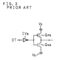
- FIG. 3 is a circuit diagram showing a common configuration of each of the non-inverting buffers B1, B2 ⁇ B n .
- the output side of the inverter IV B to which each bit of the digital signal DT is inputted, is connected to a gate of the P-channel MOS transistor Q PB and to a gate of the N-channel MOS transistor Q NB which are connected seriously.
- a power potential V D is given, and to the other end, a ground potential V S is given. From the connecting node of the MOS transistors Q PB and Q NB , a digital signal is outputted.
- the digital/analog converting circuit 8 performs digital/analog conversion.
- the ON/OFF control signal S C becomes in "L” level and all of the inputs of the non-inverting buffers B1, B2 ⁇ B n are in "L” level, the digital/analog conversion is not performed.
- the ON/OFF control signal S C is in "H” level, an analog signal AN obtained by converting a digital signal is outputted from the switching circuit 9, and when the ON/OFF control signal S C is in "L” level, the analog signal AN is not to be outputted from the switching circuit 9.
- the present invention has been devised in consideration of such problems as aforementioned which the so-called R-2R type digital/analog converting circuit has, and the object of the invention is to provide a digital/analog converting circuit capable of switching the output/non-output of an analog signal obtained by converting a digital signal and reducing the nonlinearly error by making the voltage level of an analog signal change linearly for the change of a digital signal.
- the digital/analog converting circuit related to the invention is the so-called R-2R type digital/analog converting circuit, and is provided with each first switching element capable of being in the non-output state and positioned at the input side of a each resistance to which a signal of each bit of a digital signal is inputted, and with a second switching element capable of being in the non-output state and positioned between a group of resistances connecting the output sides of the aforementioned resistances in a state of a ladder and a positive or negative reference potential, and is so configured that the first switching elements and the second switching element are switched to an output state or non-output state respectively by a control signal.
- each of the first switching elements and the second switching element when each of the first switching elements and the second switching element are in the output state, each of the first switching elements selects positive or negative reference potential corresponding to an inputted signal of each bit to output it to each resistance, and the second switching element connects the resistance to the reference potential. Therefore, an analog signal is outputted according to the positive or negative reference potential selected by each first switching element.
- each first switching element when each of the first switching elements and the second switching element are in the non-output state, each first switching element does not output positive or negative reference potential to each resistance, and the second switching element cuts out the resistance from the reference potential. Thereby, a digital signal is not converted to an analog signal. Accordingly, the output/non-output of an analog signal can be switched, and electric current does not flow through a resistance in the non-output state.
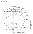
- FIG. 5 is a circuit diagram showing an example of a configuration of the digital/analog converting circuit related to the invention.
- a character in each () shows a resistance value.
- Reference character DT designates a digital signal, which is composed of a plural bits (n bits) of the MSB to the LSB.
- Reference characters B1, B2 ⁇ B n respectively show non-inverting buffers each being a three-state buffer whose output resistance value is r. To each one end of these non-inverting buffers B1, B2 ⁇ B n , a signal of each bit of the aforementioned digital signal DT is inputted.
- Each of the reference characters D1, D2 ⁇ D n designates a resistance of resistance value of 2R-r. To one end of each of the resistances D1, D2 ⁇ D n , the output side (the other end) of each of the aforementioned non-inverting buffers B1, B2 ⁇ B n is connected.
- the other end of the resistance D1 is grounded through a serial circuit composed of resistances E1, E2 ⁇ each having a resistance value of R, resistance D n+1 having a resistance value of 2R-r and a MOS transistor 20.
- the other end of the resistance D2 is connected to a connecting node between the resistances E1 and E2.
- the other end of the resistance D n is connected to the one end of the side to which the MOS transistor 20 of the resistance D n+1 is not connected.
- an analog signal AN is outputted.
- an ON/OFF control signal S B is given to control terminals of the non-inverting buffers B1, B2 ⁇ B n and a gate of the MOS transistor 20, an ON/OFF control signal S B is given.
- Resistances values of the resistances D1, D2 ⁇ D n+1 is selected in consideration of the on-resistance of the non-inverting buffers B1, B2 ⁇ B n , and the MOS transistor 20. That is, on-resistance of each of the non-inverting buffers B1, B2 ⁇ B n and on-resistance of the MOS transistor 20 are made equal.
- a digital/analog conversion circuit 12 is composed of the non-inverting buffers B1, B2 ⁇ B n , the resistances D1, D2 ⁇ D n , the resistances E1, E2 ⁇ and the MOS transistor 20.
- FIG. 6 is a circuit diagram showing a common configuration of each of the non-inverting buffers B1, B2 ⁇ B n .
- a signal of each bit of the digital signal DT is inputted to one input terminal of a NAND circuit ND of CMOS configuration and to one input terminal of a NOR circuit NR of CMOS configuration.
- the ON/OFF control signal S B is inputted to the other input terminal of the NAND circuit ND and an inverter I.
- the output of the inverter I is inputted to the other input terminal of the NOR circuit NR.
- the output of the HAND circuit ND is inputted to a gate of a P channel transistor Q PB , and the output of the NOR circuit NR to a gate of an N channel transistor Q NB .
- a potential V D which is a positive reference potential is given, and to the other end, a potential V S which is a negative reference potential is given.
- the potential V D or V S is outputted from the connecting node of the transistor Q PB and the transistor Q NB .
- V D or V S outputted from each of the non-inverting buffers B1, B2 ⁇ B n is given to a resistance group composed of the resistances D1, D2 ⁇ D n , D n+1 and the resistances E1, E2 ⁇ , so that the digital signal DT is converted into the analog signal AN.
- an analog signal of 2 n steps of voltage level of 0, V D /2 n ⁇ ⁇ (2 n -1)V D ⁇ /2 n is obtained.
- electrical characteristic is considered when the digital/analog converting circuit is in the operation of digital/analog conversion.
- an analog signal obtained by converting a digital signal by the digital/analog conversion circuit 12 is given to a load resistance L shown in FIG. 5
- electric potential does not drop in the digital/analog converting circuit 12 when the resistance value of the load resistance L is infinite (no load), and the analog potential after digital/analog conversion is given intact to the load resistance L.
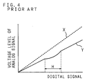
- the digital/analog conversion characteristic is a linear characteristic as shown by a broken line X in FIG. 7.
- the output potential of the digital/analog converting circuit 12 becomes output potential R L /(R+R L ) at the time of no load since the output resistance of the digital/analog converting circuit 12 is R.
- R L is a resistance value of the load resistance L.
- the digital/analog conversion characteristic is the one shown by a solid line W in FIG. 7, which is lowered a little in full-scale as compared with the case of the broken line X showing the digital/analog conversion characteristic when the resistance value of the load resistance L is infinite and causes a full-scale error.
- FIG. 8 is a circuit diagram showing a configuration of another embodiment of the digital/analog conversion circuit related to the invention.
- signal outputting means V HL for outputting a signal of "H" level or “L” level is provided, and the output thereof is inputted to one end of a non-inverting buffer B n+2 provided in place of the MOS transistor 20.
- the other end of the non-inverting buffer B n+2 is connected to one end of the resistance D n+1 .
- the non-inverting buffer B n+1 has a configuration as shown in FIG. 6 similarly to the other non-inverting buffers B1, B2 ⁇ B n , and to the control terminal thereof, the ON/OFF control signal S B is inputted.
- the configuration other than that shown in FIG. 8 is same as the configuration shown in FIG. 5, and the same parts are designated by the same reference characters and the explanation therefor will be omitted.
- FIG. 9 is a block diagram showing a configuration of a one-chip microcomputer of CMOS configuration in which the digital/analog converting circuit of the invention is built in.
- the CPU 3, ROM 4, RAM 5, data register 6, D/A converter select register 7, digital/analog converting circuit 12, digital signal input/output port 10 and bus 11 are built in.
- the CPU 3, ROM 4, RAM 5, data register 6, D/A converter select register 7 and digital signal input/output port 10 are connected to each other by a bus 11.
- the data held by the D/A converter select register 7 is given to the digital/analog converting circuit 12 and the digital signal input/output port 10.
- the digital data held by the data register 6 is inputted to the digital/analog converting circuit 12, and the analog signal after digital/analog conversion is outputted to the outside from the signal input/output terminal 2.
- the digital signal inputted from the outside to the signal input/output terminal 2 is inputted to the digital signal input/output port 10.
- the digital signal input/output port 10 becomes in the enable state and the digital/analog converting circuit 12 becomes in the non output state respectively. Accordingly, the function of the signal input/output terminal 2 becomes the one for inputting/outputting a digital signal through the digital signal input/output port 10.
- the MOS transistor 20 or the non-inverting buffer B n+1 in the digital/analog converting circuit 12 becomes in the non-output state, as aforementioned. Therefore, current does not flow through the MOS transistor 20 or the non-inverting buffer B n+1 . Accordingly, even when a digital signal is inputted from the outside to the signal input/output terminal 2 while an analog signal is not outputted, there is no possibility that the voltage level of the digital signal is not changed.
- the terminal of the digital/analog converting circuit is also used for the digital signal input/output port, however, the terminal of the digital/analog converting circuit may also be used for the digital signal input port or the digital signal output port.
- the digital/analog converting circuit is built in a one-chip microcomputer, however, this is only an example, and it is a matter of course that the same effect can be obtained by applying the digital/analog converting circuit to other than the one-chip microcomputer.
- a digital signal is inputted to a non-inverting buffer, however, it is possible to use an inverting buffer in place of a non-inverting buffer.
- the digital/analog converting circuit since the digital/analog converting circuit is not so configured that the output/non-output of an analog signal obtained by converting a digital signal is switched by the switching circuit using a transistor, the linearity of the digital/analog conversion characteristic is not to be damaged by the on-resistance of the transistor. Therefore, a digital signal can be converted into an analog signal in high accuracy all over the region in which a digital signal changes.
Landscapes
- Engineering & Computer Science (AREA)
- Theoretical Computer Science (AREA)
- Analogue/Digital Conversion (AREA)
Applications Claiming Priority (2)
| Application Number | Priority Date | Filing Date | Title |
|---|---|---|---|
| JP33070593A JP3551200B2 (ja) | 1993-12-27 | 1993-12-27 | デジタル/アナログ変換回路 |
| JP330705/93 | 1993-12-27 |
Publications (2)
| Publication Number | Publication Date |
|---|---|
| EP0660529A1 true EP0660529A1 (de) | 1995-06-28 |
| EP0660529B1 EP0660529B1 (de) | 1998-11-11 |
Family
ID=18235643
Family Applications (1)
| Application Number | Title | Priority Date | Filing Date |
|---|---|---|---|
| EP94118890A Expired - Lifetime EP0660529B1 (de) | 1993-12-27 | 1994-11-30 | Digital/Analogwandlerschaltung |
Country Status (5)
| Country | Link |
|---|---|
| US (1) | US5602552A (de) |
| EP (1) | EP0660529B1 (de) |
| JP (1) | JP3551200B2 (de) |
| KR (1) | KR0149707B1 (de) |
| DE (1) | DE69414538T2 (de) |
Cited By (1)
| Publication number | Priority date | Publication date | Assignee | Title |
|---|---|---|---|---|
| EP2592755A3 (de) * | 2011-11-14 | 2014-03-05 | Semtech Corporation | Resistive Digital-Analog-Wandlung |
Families Citing this family (4)
| Publication number | Priority date | Publication date | Assignee | Title |
|---|---|---|---|---|
| US5815104A (en) * | 1997-03-20 | 1998-09-29 | Sigmatel, Inc. | Method and apparatus for digital to analog conversion |
| JP4116190B2 (ja) * | 1999-05-06 | 2008-07-09 | 日本テキサス・インスツルメンツ株式会社 | Da変換器及びad変換器 |
| CN112803948B (zh) | 2020-12-31 | 2022-05-03 | 深圳市紫光同创电子有限公司 | 数模转换电路和方法 |
| US20250292637A1 (en) * | 2024-03-18 | 2025-09-18 | Ohio INTX Cooperative | System, method, and device for converting digital data from a controller area network chip to analog signals for display on a vehicle gauge |
Citations (4)
| Publication number | Priority date | Publication date | Assignee | Title |
|---|---|---|---|---|
| EP0177909A2 (de) * | 1984-10-09 | 1986-04-16 | Yamaha Corporation | Digital-Analogwandler |
| WO1986005609A1 (en) * | 1985-03-11 | 1986-09-25 | Ncr Corporation | Digital to analog conversion apparatus |
| JPS6333014A (ja) * | 1986-07-26 | 1988-02-12 | Canon Inc | デジタルアナログ変換回路 |
| EP0414593A2 (de) * | 1989-08-19 | 1991-02-27 | Fujitsu Limited | Digital-Analog-Wandler mit Widerstandsleiterschaltung |
Family Cites Families (3)
| Publication number | Priority date | Publication date | Assignee | Title |
|---|---|---|---|---|
| DE3145889A1 (de) * | 1981-11-19 | 1983-05-26 | Siemens AG, 1000 Berlin und 8000 München | Integrierbarer digital/analog-wandler |
| US4833473A (en) * | 1987-10-05 | 1989-05-23 | Harris Semiconductor Patents, Inc. | Digital to analog converter with switch function compensation |
| JPH0734542B2 (ja) * | 1988-06-29 | 1995-04-12 | 日本電気株式会社 | D−a変換回路 |
-
1993
- 1993-12-27 JP JP33070593A patent/JP3551200B2/ja not_active Expired - Fee Related
-
1994
- 1994-11-22 US US08/345,754 patent/US5602552A/en not_active Expired - Fee Related
- 1994-11-30 EP EP94118890A patent/EP0660529B1/de not_active Expired - Lifetime
- 1994-11-30 DE DE69414538T patent/DE69414538T2/de not_active Expired - Fee Related
- 1994-12-26 KR KR1019940036806A patent/KR0149707B1/ko not_active Expired - Fee Related
Patent Citations (4)
| Publication number | Priority date | Publication date | Assignee | Title |
|---|---|---|---|---|
| EP0177909A2 (de) * | 1984-10-09 | 1986-04-16 | Yamaha Corporation | Digital-Analogwandler |
| WO1986005609A1 (en) * | 1985-03-11 | 1986-09-25 | Ncr Corporation | Digital to analog conversion apparatus |
| JPS6333014A (ja) * | 1986-07-26 | 1988-02-12 | Canon Inc | デジタルアナログ変換回路 |
| EP0414593A2 (de) * | 1989-08-19 | 1991-02-27 | Fujitsu Limited | Digital-Analog-Wandler mit Widerstandsleiterschaltung |
Non-Patent Citations (1)
| Title |
|---|
| PATENT ABSTRACTS OF JAPAN vol. 12, no. 244 (E - 631) 9 July 1988 (1988-07-09) * |
Cited By (1)
| Publication number | Priority date | Publication date | Assignee | Title |
|---|---|---|---|---|
| EP2592755A3 (de) * | 2011-11-14 | 2014-03-05 | Semtech Corporation | Resistive Digital-Analog-Wandlung |
Also Published As
| Publication number | Publication date |
|---|---|
| DE69414538T2 (de) | 1999-05-06 |
| KR0149707B1 (ko) | 1998-12-15 |
| JPH07193504A (ja) | 1995-07-28 |
| EP0660529B1 (de) | 1998-11-11 |
| US5602552A (en) | 1997-02-11 |
| KR950022163A (ko) | 1995-07-28 |
| JP3551200B2 (ja) | 2004-08-04 |
| DE69414538D1 (de) | 1998-12-17 |
Similar Documents
| Publication | Publication Date | Title |
|---|---|---|
| US6346899B1 (en) | Analog current mode D/A converter using transconductors | |
| US4695826A (en) | High accuracy digital-to-analog converter having symmetrical current source switching | |
| US4045793A (en) | Digital to analog converter | |
| EP0378840A2 (de) | Digital-Analogwandler mit einer einzigen Widerstandskette und mit veränderbarer Spannung darüber | |
| EP0466145B1 (de) | Digitalanalogwandler | |
| US8937568B2 (en) | D/A converter | |
| US5894281A (en) | Digital-to-analog converter utilizing MOS transistor switching circuit with accompanying dummy gates to set same effective gate capacitance | |
| US6181265B1 (en) | Non-linear digital-to-analog converter | |
| EP0660529A1 (de) | Digital Analogwandlungsschaltung | |
| US7375669B2 (en) | Digital/analog converter | |
| US7239171B1 (en) | Techniques for providing multiple termination impedance values to pins on an integrated circuit | |
| US6999016B2 (en) | D/A converter and semiconductor device | |
| KR100514320B1 (ko) | 디지털/아날로그 변환기 | |
| US20030043065A1 (en) | Precise differential voltage interpolation analog-to-digital converter having double interpolation using nonlinear resistors | |
| JP2006173721A (ja) | 電流源セルおよびそれを用いたd/aコンバータ | |
| US5220306A (en) | Digital signal comparator for comparing n-bit binary signals | |
| US4803461A (en) | R-2R type D/A converter circuit | |
| US6140953A (en) | D/A converting apparatus with independent D/A converter controlled reference signals | |
| US20040125004A1 (en) | D/A converter for converting plurality of digital signals simultaneously | |
| US7358886B2 (en) | Voltage output digital-to-analog converter circuit | |
| EP0210697A2 (de) | Bildung einer digitalen Darstellung des Zeitintegrals eines elektrischen Stromes | |
| US7342526B2 (en) | Digital-to-analog converter using plural transistors having the same operating characteristics | |
| US5657018A (en) | Bar graph decoder outputting thermometer code | |
| JPH10215179A (ja) | D/aコンバータ | |
| EP0177909A2 (de) | Digital-Analogwandler |
Legal Events
| Date | Code | Title | Description |
|---|---|---|---|
| PUAI | Public reference made under article 153(3) epc to a published international application that has entered the european phase |
Free format text: ORIGINAL CODE: 0009012 |
|
| AK | Designated contracting states |
Kind code of ref document: A1 Designated state(s): DE FR GB |
|
| 17P | Request for examination filed |
Effective date: 19950620 |
|
| GRAG | Despatch of communication of intention to grant |
Free format text: ORIGINAL CODE: EPIDOS AGRA |
|
| 17Q | First examination report despatched |
Effective date: 19980506 |
|
| GRAG | Despatch of communication of intention to grant |
Free format text: ORIGINAL CODE: EPIDOS AGRA |
|
| GRAH | Despatch of communication of intention to grant a patent |
Free format text: ORIGINAL CODE: EPIDOS IGRA |
|
| GRAH | Despatch of communication of intention to grant a patent |
Free format text: ORIGINAL CODE: EPIDOS IGRA |
|
| GRAH | Despatch of communication of intention to grant a patent |
Free format text: ORIGINAL CODE: EPIDOS IGRA |
|
| GRAA | (expected) grant |
Free format text: ORIGINAL CODE: 0009210 |
|
| AK | Designated contracting states |
Kind code of ref document: B1 Designated state(s): DE FR GB |
|
| REF | Corresponds to: |
Ref document number: 69414538 Country of ref document: DE Date of ref document: 19981217 |
|
| ET | Fr: translation filed | ||
| PLBE | No opposition filed within time limit |
Free format text: ORIGINAL CODE: 0009261 |
|
| STAA | Information on the status of an ep patent application or granted ep patent |
Free format text: STATUS: NO OPPOSITION FILED WITHIN TIME LIMIT |
|
| 26N | No opposition filed | ||
| REG | Reference to a national code |
Ref country code: GB Ref legal event code: IF02 |
|
| PGFP | Annual fee paid to national office [announced via postgrant information from national office to epo] |
Ref country code: FR Payment date: 20061108 Year of fee payment: 13 |
|
| PGFP | Annual fee paid to national office [announced via postgrant information from national office to epo] |
Ref country code: DE Payment date: 20061123 Year of fee payment: 13 |
|
| PGFP | Annual fee paid to national office [announced via postgrant information from national office to epo] |
Ref country code: GB Payment date: 20061129 Year of fee payment: 13 |
|
| GBPC | Gb: european patent ceased through non-payment of renewal fee |
Effective date: 20071130 |
|
| PG25 | Lapsed in a contracting state [announced via postgrant information from national office to epo] |
Ref country code: DE Free format text: LAPSE BECAUSE OF NON-PAYMENT OF DUE FEES Effective date: 20080603 |
|
| REG | Reference to a national code |
Ref country code: FR Ref legal event code: ST Effective date: 20080930 |
|
| PG25 | Lapsed in a contracting state [announced via postgrant information from national office to epo] |
Ref country code: GB Free format text: LAPSE BECAUSE OF NON-PAYMENT OF DUE FEES Effective date: 20071130 |
|
| PG25 | Lapsed in a contracting state [announced via postgrant information from national office to epo] |
Ref country code: FR Free format text: LAPSE BECAUSE OF NON-PAYMENT OF DUE FEES Effective date: 20071130 |