EP0661642A2 - Mikrorechner mit Lesespeicher - Google Patents
Mikrorechner mit Lesespeicher Download PDFInfo
- Publication number
- EP0661642A2 EP0661642A2 EP94120690A EP94120690A EP0661642A2 EP 0661642 A2 EP0661642 A2 EP 0661642A2 EP 94120690 A EP94120690 A EP 94120690A EP 94120690 A EP94120690 A EP 94120690A EP 0661642 A2 EP0661642 A2 EP 0661642A2
- Authority
- EP
- European Patent Office
- Prior art keywords
- address
- program memory
- internal program
- present
- instruction
- Prior art date
- Legal status (The legal status is an assumption and is not a legal conclusion. Google has not performed a legal analysis and makes no representation as to the accuracy of the status listed.)
- Granted
Links
Images




Classifications
-
- G—PHYSICS
- G06—COMPUTING OR CALCULATING; COUNTING
- G06F—ELECTRIC DIGITAL DATA PROCESSING
- G06F12/00—Accessing, addressing or allocating within memory systems or architectures
- G06F12/14—Protection against unauthorised use of memory or access to memory
- G06F12/1416—Protection against unauthorised use of memory or access to memory by checking the object accessibility, e.g. type of access defined by the memory independently of subject rights
- G06F12/1425—Protection against unauthorised use of memory or access to memory by checking the object accessibility, e.g. type of access defined by the memory independently of subject rights the protection being physical, e.g. cell, word, block
- G06F12/1441—Protection against unauthorised use of memory or access to memory by checking the object accessibility, e.g. type of access defined by the memory independently of subject rights the protection being physical, e.g. cell, word, block for a range
-
- G—PHYSICS
- G06—COMPUTING OR CALCULATING; COUNTING
- G06F—ELECTRIC DIGITAL DATA PROCESSING
- G06F12/00—Accessing, addressing or allocating within memory systems or architectures
- G06F12/14—Protection against unauthorised use of memory or access to memory
-
- G—PHYSICS
- G06—COMPUTING OR CALCULATING; COUNTING
- G06F—ELECTRIC DIGITAL DATA PROCESSING
- G06F12/00—Accessing, addressing or allocating within memory systems or architectures
- G06F12/14—Protection against unauthorised use of memory or access to memory
- G06F12/1416—Protection against unauthorised use of memory or access to memory by checking the object accessibility, e.g. type of access defined by the memory independently of subject rights
- G06F12/1425—Protection against unauthorised use of memory or access to memory by checking the object accessibility, e.g. type of access defined by the memory independently of subject rights the protection being physical, e.g. cell, word, block
- G06F12/1433—Protection against unauthorised use of memory or access to memory by checking the object accessibility, e.g. type of access defined by the memory independently of subject rights the protection being physical, e.g. cell, word, block for a module or a part of a module
Definitions
- the present invention relates to a microcomputer and, more particularly, to a microcomputer to which an external program memory can be connected for expansion.
- microcomputers to each of which an external program memory can be connected for expansion are popularly used Most microcomputers include internal data memories in each of which a program can be written by a central processing unit (to be abbreviated as a CPU hereinafter), a direct memory access controller (to be abbreviated as a DMAC hereinafter), or the like.
- a central processing unit to be abbreviated as a CPU hereinafter
- a direct memory access controller to be abbreviated as a DMAC hereinafter
- the contents of an internal program memory can be read out to an external circuit by a program written in the external program memory or the internal data memory.
- a conventional microcomputer cannot meet such a requirement, and the contents of the internal program memory cannot be prevented from being read out by a third party.
- a third party can easily rewrite the contents of the external program memory, and can read out the contents of the internal program memory without permission of the developer of the program and the manufacturer of the microcomputer by writing a program for externally outputting the contents of the internal program memory of the microcomputer in the external program memory, and operating the microcomputer.
- the contents of the internal program memory can also be read out without consent of the developer of the program and the manufacturer of the microcomputer by writing a program for transferring the contents of the internal program memory the internal data memory of the microcomputer and then outputting the contents of the internal data memory to an external circuit by a program written by a third party in the external program memory and operating the microcomputer in place of directly outputting the contents of the internal program memory to an external circuit.
- an object of the present invention to provide a microcomputer which can inhibit a third party from reading out the contents of an internal program memory of the microcomputer.
- a microcomputer which has an internal program memory and to which an external program memory can be connected for expansion, comprises detection means for detecting if an address read out from a register for holding the address used upon fetching an instruction from the program memory is present in an address space of the internal program memory, and means for, when it is detected that the address is not present in the address space of the internal program memory, inhibiting to read the contents of the internal program memory by the instruction.
- the detection means detects if the address used upon fetching of an instruction from the program memory is present in the address space of the internal program memory, and when it is detected that the address is not present in the address space of the internal program memory, a read access of the contents of the internal program memory is inhibited. For this reason, the contents of the internal program memory can be prevented from being read out by a program (instructions) stored in a memory other than the internal program memory, e.g., the external program memory, an internal data memory, or the like.
- the microcomputer may comprise address changing means for changing the read address to an address other than that in the address space of the internal program memory, or may comprise data changing means for changing read data (the contents of the internal program memory) to other data (for example, zero) or may comprise instruction execution halt means for halting execution of the instruction, or may comprise interrupt generation means for generating interrupt.
- the microcomputer may comprise means for, when it is detected that the address is not present in specific address spaces of the internal program memory, inhibiting a read access of the contents of the internal program memory, or may comprise address changing means for changing the address to an address other than that in the address spaces of the internal program memory, or may comprise data changing means for changing read data (the contents of the internal program memory) to other data (for example, zero) or instruction execution halt means for halting execution of the instruction, or may comprise interrupt generation means for generating interrupt in such a case.
- a microcomputer has the following feature. That is, when the address stored an instruction for reading out the contents of an internal program memory is not present in the address space (may be either the entire space or specific spaces) of the internal program memory, a read access of the contents of the internal program memory by this instruction is inhibited, the read address is changed, or the execution of the instruction is halted.
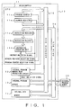
- FIG. 1 shows the arrangement of a microcomputer according to an embodiment of the present invention.
- a microcomputer 10 incorporates a CPU 11 having a program counter 11a, an instruction decoder 11b, an instruction register 11c, an instruction execution unit 11d, and an address register 11e; an internal program memory read protection circuit 12; an internal program memory 13; and a data memory 14, and also connects an external program memory 20.
- the program counter 11a holds an address indicating the location where an instruction to be executed, and it outputs the address onto an address bus 15.
- the address register 11e outputs an address indicating the location where a program or data is stored onto the address bus 15 when an instruction is executed, and the program or data is read out in accordance with the instruction.
- the instruction register 11c fetches, via a data bus 16, an instruction output from the location (the internal program memory 13 or the external program memory 20) indicated by the address output from the program counter 11a, and temporarily holds the fetched Instruction.
- the instruction decoder 11b receives the instruction held by and output from the instruction register 11c, and decodes the fetched instruction.
- the instruction execution unit 11d receives the decoding result from the instruction decoder 11b, and executes the instruction. At this time, the instruction execution unit 11d outputs an instruction fetch signal to the internal program memory read protection circuit 12 and the instruction register 11c, as will be described later.
- the instruction execution unit 11d Upon execution of an instruction, when the next required address based on the instruction is present in the program counter 11a, the instruction execution unit 11d outputs a program counter selection signal to the program counter 11a; when the next required address is present in the address register 11e, the unit 11d outputs an address register selection signal to the address register 11e.
- the internal program memory read protection circuit 12 When the internal program memory read protection circuit 12 receives an instruction fetch signal from the instruction execution unit 11d, it checks if the address indicating the location where the instruction at that time is stored is present in the address space of the internal program memory 13, and also checks if the address indicating the storage location of a program or data to be read out in accordance with the instruction is present in the address space of the internal program memory 13. Only when the address of the instruction is not present in the address space of the internal program memory 13 and the address of the program or data to be read out is present in the address space of the internal program memory 13, the protection circuit 12 outputs a read inhibition signal to the internal program memory 13.
- the internal program memory 13 is an internal memory for storing a program or data.
- the internal data memory 14 is usually an internal memory for storing data.
- the external program memory 20 is an external memory for storing a program or data.
- An address output from the program counter 11a in the CPU 11 via the address bus 15 is supplied to the internal program memory read protection circuit 12, the internal program memory 13, the internal data memory 14, and the external program memory 20.
- a program or data stored in one of these memories indicated by the address is read out as an instruction, the readout instruction is held in the instruction register 11c via the data bus 16, and the instruction is decoded by the instruction decoder 11b.
- an instruction fetch signal from the instruction execution unit 11d is output to the internal program memory read protection circuit 12.
- the internal program memory read protection circuit 12 checks if the address of the instruction is present in the address space of the internal program memory 13, and also checks if the address of the program or data to be read out by the instruction is present in the address space of the internal program memory 13.
- the internal program memory read protection circuit 12 determines that the address of the instruction is not present in the address space of the internal program memory 13, and the address of the program or data to be read out by the instruction is present in the address space of the internal program memory 13, the internal program memory read protection circuit 12 outputs a read inhibition signal to the internal program memory 13, and a read access of the program or data is inhibited.
- Fig. 2 shows an example of the detailed arrangement of the internal program memory read protection circuit 12.
- the protection circuit 12 comprises an address decoder 12a, a memory element 12b, and an AND gate 12c.
- the address decoder 12a receives an address transferred from the address bus 15, detects if the received address is present in the address space of the internal program memory 13, and outputs the detection result.
- an instruction fetch signal is output from the instruction execution unit 11d, and is supplied to the internal program memory read protection circuit 12.
- the detection result output from the address decoder 12a is stored in the memory element 12b.
- the output from the memory element 12b and the output from the address decoder 12a are input to the AND gate 12c.
- the AND gate 12c outputs a read inhibition signal, and supplied it to the internal program memory 13.
- the memory element 12b When the address is present in the address space of the internal program memory 13, the memory element 12b stores data of logic "1", and at this time, the memory element 12b outputs inverted data of logic "0" to the AND gate 12c. When the address is not present in the address space of the internal program memory 13, the memory element 12b stores data of logic "0", and outputs data of logic "1" to the AND gate 12c.
- an address transferred from the address bus is input to the address decoder 12a.
- This address indicates a location where a program or data to be read out by the instruction is stored,
- the address decoder 12a checks if this address is present in the address space of the internal program memory 13. When the address is present, data of logic "1" is output from the address decoder 12a to the AND gate 12c; otherwise, data of logic "0" is output from the address decoder 12a to the AND gate 12c.
- the memory element 12b When the address of the instruction is not present in the address space of the internal program memory 13, and the address of the program or data to be read out by the instruction is present in the address space of the internal program memory 13, the memory element 12b outputs data of logic "1", the address decoder 12a outputs data of logic "1”, and these data are output to the AND gate 12c. As a result, a read inhibition signal of logic "1" is output from the AND gate 12c to the internal program memory 13, thus inhibiting a read access by this instruction.
- the memory element 12b when the address of the instruction is present in the address space of the internal program memory 13, the memory element 12b outputs data of logic "0", and supplies it to the AND gate 12c. Therefore, independently of whether or not the address of the program or data to be read out is present in the address space of the internal program memory 13, the AND gate 12c outputs a read inhibition signal of logic "0", and supplies it to the internal program memory 13.
- Fig. 3 is a timing chart of the signals in the embodiment shown in Fig. 2.
- "F” in “CPU operation” represents an instruction fetch operation for reading out an instruction from a memory and holding the readout instruction by the instruction register 11c
- "D” represents an instruction decode operation for decoding an instruction using the instruction decoder 11b
- "E” represents an instruction execution operation for executing an instruction using the instruction execution unit 11d.
- a period 101 represents a period in which when the address of an instruction is present in the address space of the internal program memory 13, the instruction is fetched and decoded.
- a period 102 represents a period in which when the address of a program or data to be read out in accordance with the instruction is present in the address space of the internal program memory 13, a read access is permitted.
- a period 103 represents a period in which when the address of an instruction is not present in the address space of the internal program memory 13, but is present in the address space of the external program memory 20, the instruction is fetched and decoded
- a period 104 represents a period in which when the address of a program or data to be read out in accordance with the instruction is present in the address space of the internal program memory 13, a read access is inhibited.
- the periods 101 to 104 will be described in detail below.
- the CPU 11 outputs an address from the program counter 11a to the address bus 15 to fetch the next instruction to be executed, This address is present in the address space of the internal program memory 13.
- data of logic "1" is output from the address decoder 12a in the internal program memory read protection circuit 12, and is stored in the memory element 12b.
- the memory element 12b outputs data of logic "0". Therefore, the output from the AND gate 12c goes to logic "0", and a read access of the contents of the internal program memory 13 is permitted.
- An instruction is read out from the internal program memory designated by the address, and is held in the instruction register 11c in the CPU 11. The instruction is then decoded by the instruction decoder 11b.
- the instruction decoded by the instruction decoder 11b is executed by the instruction execution unit 11d.
- the contents of the internal program memory 13 are read out onto the data bus 16 in accordance with the address transferred from, e.g., the address register 11e via the address bus 15.
- a read access of the contents of the internal program memory 13 is permitted since the read inhibition signal is at logic"0".
- an instruction stored in a memory other than the internal program memory 13, e.g., the external program memory 20 is used in an attempt to read out the contents of the internal program memory 13.
- the CPU 11 outputs an address from the program counter 11a to the address bus 15 to fetch the next instruction to be executed. This address is not present in the address space of the internal program memory 13. Therefore, data of logic "0" is output from the address decoder 12a in the internal program memory read protection circuit 12, and is stored in the memory element 12b. Then, the memory element 12b outputs data of logic "1" to the AND gate 12c.
- An instruction is read out from the external program memory designated by the address, and is held in the instruction register 11c in the CPU 11. Then, the held instruction is decoded by the instruction decoder 11b.
- the instruction decoded by the instruction decoder 11b is executed by the instruction execution unit 11d.
- the CPU 11 outputs the address present in the address space of the internal program memory 13 from, e.g., the address register 11e onto the address bus 15.
- the address of a program or data to be read out is supplied to the address decoder 12a in the internal program memory read protection circuit 12, and the address decoder 12a outputs data of logic "1" to the AND gate 12c.
- the output from the AND gate 12c goes to logic "1", and a read access of the contents of the internal program memory 13 is inhibited. As a result, the contents of the internal program memory 13 are not read out.
- the contents of the internal program memory cannot be read out using an instruction stored in a memory outside the address space of the internal program memory, and can be prevented from being disclosed to a third party.
- an internal program memory 23 may incorporate an address decoder 23a in place of incorporating the address decoder in an internal program memory read protection circuit 22.
- the address decoder 23a in the internal program memory 23 decodes the address space of a memory cell 23b, and generates and outputs a chip (memory cell) select signal.
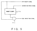
- Fig. 5 shows an example of the arrangement of the internal program memory read protection circuit 22 in this case
- the internal program memory read protection circuit 22 has a memory element 22b and an AND gate 22c.
- the memory element 22b receives an instruction fetch signal and a chip select signal.
- the instruction fetch signal is output from the instruction execution unit 11d, and the chip select signal is output from the address decoder 23a in the internal program memory 23.
- the address decoder 23a When the address is present in the address space of the internal program memory 23, the address decoder 23a outputs a chip select signal of logic "1"; when the address is present outside the address space of the internal program memory 23, the decoder 23a outputs a chip select signal of logic "0".
- the memory element 22b stores the chip select signal at that time in synchronism with the reception timing of the instruction fetch signal.
- a chip select signal of logic "1” is input to the memory element 22b, a signal of logic "0” is output and is supplied to the AND gate 22c; when a chip select signal of logic "0” is input, a signal of logic "1” is output and is supplied to the AND gate 22c.
- an address indicating a location where a program or data to be read out is stored is input to the address decoder 23a.
- a chip select signal of logic "0" is output from the address decoder 23a, and is input to the AND gate 22c.
- the AND gate 22c outputs a read inhibition signal of logic "0" independently of whether or not the address of the read instruction is present in the address space of the internal program memory 23, a read access is permitted.
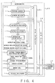
- Fig. 6 shows the arrangement of a microcomputer 30 according to another embodiment of the present invention.
- the microcomputer 30 incorporates a CPU 31 having a program counter 11a, an instruction decoder 11b, an instruction register 11c, an instruction execution unit 31d, and an address register 11e; an internal program memory read protection circuit 32; a program memory 13; and a data memory 14, and also connects an external program memory 20.
- An address output from the program counter 11a or the address register 11e via an address bus 35 is supplied from the CPU 31 to the internal program memory read protection circuit 32, the internal program memory 13, the internal data memory 14, and the external program memory 20.
- An instruction is read out from a memory designated by the address output from the program counter 11a, and is held in the instruction register 11c via a data bus 16.
- the instruction held in the instruction register 11c is decoded by the instruction decoder 11b, and is executed by the instruction execution unit 31d.
- the internal program memory read protection circuit 32 checks if the address supplied from the address register 11e via the address bus 35 is present in the address space of the internal program memory 13. Only when the address indicating a location where the instruction is stored is not present in the address space of the internal program memory 13, and the address indicating a location where a program or data to be read out in accordance with the instruction is stored is present in the address space of the internal program memory 13, a read inhibition signal of logic "1" is output from the internal program memory read protection circuit 32, and is supplied to the instruction execution unit 31d.
- the read inhibition signal of logic "1" corresponds to an instruction execution halt command signal in this embodiment, and when this signal is supplied to the instruction execution unit 31d, execution of an instruction is halted.
- the read inhibition signal is supplied to the instruction execution unit 31d.
- the read inhibition signal may he supplied to the instruction decoder 11b. in this case, when a read inhibition signal of logic "1" is supplied to the instruction decoder 11b, the decode operation of the instruction is halted.
- FIG. 7 shows the arrangement of a microcomputer according to still another embodiment of the present invention.
- a microcomputer 40 shown in Fig. 7 incorporates a CPU 11 having a program counter 11a, an instruction decoder 11b, an instruction register 11c, an instruction execution unit 11d, and an address register 11e; an internal program memory read protection circuit 42; a program memory 13; and a data memory 14, and also connects an external program memory 20.
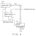
- FIG. 8 shows an example of the circuit arrangement of the internal program memory read protection circuit 42.
- the internal program memory read protection circuit 42 comprises an address decoder 42a, a memory element 42b, an AND gate 42c, and an address changing circuit 42d.
- the memory element 42b when an address supplied from the program counter 11a is present in the address space of the internal program memory 13, the memory element 42b outputs data of logic "0"; otherwise, the element 42b outputs data of logic "1".
- an address indicating the storage location of a program or data to be read out by the instruction is supplied to the address decoder 42a.
- this address is present in the address space of the internal program memory 13
- data of logic "1” is output to the AND gate 42c; otherwise, data of logic "0” is output to the AND gate 42c.
- the AND gate 42c Only when the address of the instruction is not present, and the address of the program or data to be read out in accordance with the instruction is present in the address space of the internal program memory 13, the AND gate 42c outputs a read inhibition signal of logic "1".
- the circuit 42d When a read inhibition signal of logic "1" is supplied to the address changing circuit 42d, the circuit 42d outputs an address which is not present in the address space of the internal program memory 13 onto an address bus 45b (i.e., changes the address). On the contrary, when a read inhibition signal of logic "0" is supplied to the address changing circuit 42d, the circuit 42d outputs the same value as that on the address bus 45a onto the address bus 45b (i.e., does not change the address).
- the address bus 45b is connected to the internal program memory 13, the internal data memory 14, and the external program memory 20.
- the address is changed, since an address which is not present in the address space of the internal program memory 13 is output, the contents of the internal program memory 13 cannot be read out. With this control, a third party is inhibited from reading out the contents of the internal program memory 13 without permission of interested parties.
- an object to be inhibited from being read out by a third party is the entire program or data stored in the internal program memory.
- an object to be inhibited from being read out may be stored in specific address spaces of the internal program memory. In this case, the contents of the internal program memory stored outside the specific address spaces can be read out by a third party.
Landscapes
- Engineering & Computer Science (AREA)
- Theoretical Computer Science (AREA)
- Computer Security & Cryptography (AREA)
- Physics & Mathematics (AREA)
- General Engineering & Computer Science (AREA)
- General Physics & Mathematics (AREA)
- Storage Device Security (AREA)
- Executing Machine-Instructions (AREA)
- Microcomputers (AREA)
Applications Claiming Priority (3)
| Application Number | Priority Date | Filing Date | Title |
|---|---|---|---|
| JP33499793A JP3520102B2 (ja) | 1993-12-28 | 1993-12-28 | マイクロコンピュータ |
| JP334997/93 | 1993-12-28 | ||
| JP33499793 | 1993-12-28 |
Publications (3)
| Publication Number | Publication Date |
|---|---|
| EP0661642A2 true EP0661642A2 (de) | 1995-07-05 |
| EP0661642A3 EP0661642A3 (de) | 1998-04-15 |
| EP0661642B1 EP0661642B1 (de) | 2003-03-12 |
Family
ID=18283583
Family Applications (1)
| Application Number | Title | Priority Date | Filing Date |
|---|---|---|---|
| EP94120690A Expired - Lifetime EP0661642B1 (de) | 1993-12-28 | 1994-12-27 | Mikrorechner mit Speicherleseschutz |
Country Status (5)
| Country | Link |
|---|---|
| US (1) | US5680581A (de) |
| EP (1) | EP0661642B1 (de) |
| JP (1) | JP3520102B2 (de) |
| KR (1) | KR0138697B1 (de) |
| DE (1) | DE69432245T2 (de) |
Cited By (6)
| Publication number | Priority date | Publication date | Assignee | Title |
|---|---|---|---|---|
| GB2300499A (en) * | 1995-05-01 | 1996-11-06 | Nec Corp | One-chip CPU with memory protection |
| EP0859319A1 (de) * | 1997-02-14 | 1998-08-19 | Nec Corporation | Speicherzugriff-Steuerungsschaltung |
| FR2811092A1 (fr) * | 2000-06-29 | 2002-01-04 | Fujitsu Ltd | Appareil de traitement, circuit integre et module de circuit integre |
| EP1262856A3 (de) * | 2001-05-29 | 2004-03-17 | Infineon Technologies AG | Programmgesteuerte Einheit |
| EP1013026A4 (de) * | 1997-09-16 | 2004-09-08 | Information Resource Engineeri | Kryptographischer koprozessor |
| WO2009102658A1 (en) * | 2008-02-14 | 2009-08-20 | Atmel Corporation | Access rights on a memory map |
Families Citing this family (19)
| Publication number | Priority date | Publication date | Assignee | Title |
|---|---|---|---|---|
| JPH09146914A (ja) * | 1995-09-06 | 1997-06-06 | Seiko Epson Corp | シングルチップマイクロコンピュータ及びそれを内蔵した電子機器 |
| JPH09114743A (ja) * | 1995-10-16 | 1997-05-02 | Nec Corp | シングルチップ・マイクロコンピュータ |
| US5860161A (en) * | 1996-08-14 | 1999-01-12 | Advanced Micro Devices, Inc. | Microcontroller configured to indicate internal memory accesses externally |
| US5903912A (en) * | 1996-08-14 | 1999-05-11 | Advanced Micro Devices, Inc. | Microcontroller configured to convey data corresponding to internal memory accesses externally |
| WO1998022879A1 (en) * | 1996-11-15 | 1998-05-28 | Philips Electronics N.V. | A protection method against eeprom-directed intrusion into a mobile communication device that has a processor, and a device having such protection mechanism |
| JP3588529B2 (ja) * | 1997-01-28 | 2004-11-10 | 株式会社東芝 | 半導体装置およびその応用システム装置 |
| US5862148A (en) * | 1997-02-11 | 1999-01-19 | Advanced Micro Devices, Inc. | Microcontroller with improved debug capability for internal memory |
| US6049876A (en) * | 1998-02-09 | 2000-04-11 | Motorola, Inc. | Data processing system and method which detect unauthorized memory accesses |
| FR2788353B1 (fr) * | 1999-01-11 | 2001-02-23 | St Microelectronics Sa | Microprocesseur avec circuits de protection pour securiser l'acces a ses registres |
| FR2814557B1 (fr) * | 2000-09-27 | 2002-12-27 | Gemplus Card Int | Protection contre l'exploitation abusive d'une instruction dans une memoire |
| KR100396791B1 (ko) * | 2000-10-18 | 2003-09-02 | 주식회사 하이닉스반도체 | 프로그램 메모리의 액세스장치 |
| FR2823364B1 (fr) * | 2001-04-05 | 2003-06-27 | St Microelectronics Sa | Dispositif et procede de protection partielle en lecture d'une memoire non volatile |
| KR100468615B1 (ko) * | 2002-04-02 | 2005-01-31 | 매그나칩 반도체 유한회사 | 내부 프로그램 코드 보호 장치 |
| JP4347582B2 (ja) * | 2003-02-04 | 2009-10-21 | パナソニック株式会社 | 情報処理装置 |
| FR2857535A1 (fr) * | 2003-07-09 | 2005-01-14 | Atmel Corp | Procede et systeme pour brouiller le contenu d'une cellule dans un circuit integre. |
| US7281103B2 (en) * | 2003-10-01 | 2007-10-09 | Kabushiki Kaisha Toshiba | Microcomputer with a security function for accessing a program storage memory |
| US7574576B2 (en) * | 2006-12-22 | 2009-08-11 | Spansion Llc | Semiconductor device and method of controlling the same |
| KR101697446B1 (ko) | 2012-08-15 | 2017-01-17 | 시놉시스, 인크. | 임베딩된 코드에 대한 보호 스킴 |
| JP2021140555A (ja) * | 2020-03-06 | 2021-09-16 | 本田技研工業株式会社 | 半導体装置とその制御方法 |
Family Cites Families (14)
| Publication number | Priority date | Publication date | Assignee | Title |
|---|---|---|---|---|
| US4523271A (en) * | 1982-06-22 | 1985-06-11 | Levien Raphael L | Software protection method and apparatus |
| US4590552A (en) * | 1982-06-30 | 1986-05-20 | Texas Instruments Incorporated | Security bit for designating the security status of information stored in a nonvolatile memory |
| US4521853A (en) * | 1982-06-30 | 1985-06-04 | Texas Instruments Incorporated | Secure microprocessor/microcomputer with secured memory |
| US4581702A (en) * | 1983-01-10 | 1986-04-08 | International Business Machines Corporation | Critical system protection |
| JPS6068441A (ja) * | 1983-09-22 | 1985-04-19 | Fujitsu Ltd | ワンチツプ・マイクロ・コンピユ−タ |
| US5347636A (en) * | 1985-11-08 | 1994-09-13 | Nec Corporation | Data processor which efficiently accesses main memory and input/output devices |
| US5155829A (en) * | 1986-01-21 | 1992-10-13 | Harry M. Weiss | Memory system and method for protecting the contents of a ROM type memory |
| JPS62204345A (ja) * | 1986-03-05 | 1987-09-09 | Oki Electric Ind Co Ltd | マイクロコンピユ−タ |
| US5134700A (en) * | 1987-09-18 | 1992-07-28 | General Instrument Corporation | Microcomputer with internal ram security during external program mode |
| FR2621409A1 (fr) * | 1987-10-02 | 1989-04-07 | Thomson Semiconducteurs | Dispositif de protection des zones memoires d'un systeme electronique a microprocesseur |
| US5014191A (en) * | 1988-05-02 | 1991-05-07 | Padgaonkar Ajay J | Security for digital signal processor program memory |
| US5251304A (en) * | 1990-09-28 | 1993-10-05 | Motorola, Inc. | Integrated circuit microcontroller with on-chip memory and external bus interface and programmable mechanism for securing the contents of on-chip memory |
| DE69231077T2 (de) * | 1991-03-06 | 2001-02-01 | Nec Corp., Tokio/Tokyo | Einchipmikrorechner mit Schutzfuntion für den Inhalt eines internen ROM's |
| US5557743A (en) * | 1994-04-05 | 1996-09-17 | Motorola, Inc. | Protection circuit for a microprocessor |
-
1993
- 1993-12-28 JP JP33499793A patent/JP3520102B2/ja not_active Expired - Lifetime
-
1994
- 1994-12-27 EP EP94120690A patent/EP0661642B1/de not_active Expired - Lifetime
- 1994-12-27 DE DE69432245T patent/DE69432245T2/de not_active Expired - Lifetime
- 1994-12-28 US US08/364,989 patent/US5680581A/en not_active Expired - Lifetime
- 1994-12-28 KR KR1019940037894A patent/KR0138697B1/ko not_active Expired - Fee Related
Cited By (11)
| Publication number | Priority date | Publication date | Assignee | Title |
|---|---|---|---|---|
| GB2300499A (en) * | 1995-05-01 | 1996-11-06 | Nec Corp | One-chip CPU with memory protection |
| US5860123A (en) * | 1995-05-01 | 1999-01-12 | Nec Corporation | One-chip CPU |
| EP0859319A1 (de) * | 1997-02-14 | 1998-08-19 | Nec Corporation | Speicherzugriff-Steuerungsschaltung |
| US6101586A (en) * | 1997-02-14 | 2000-08-08 | Nec Corporation | Memory access control circuit |
| EP1013026A4 (de) * | 1997-09-16 | 2004-09-08 | Information Resource Engineeri | Kryptographischer koprozessor |
| FR2811092A1 (fr) * | 2000-06-29 | 2002-01-04 | Fujitsu Ltd | Appareil de traitement, circuit integre et module de circuit integre |
| EP1262856A3 (de) * | 2001-05-29 | 2004-03-17 | Infineon Technologies AG | Programmgesteuerte Einheit |
| US7228569B2 (en) | 2001-05-29 | 2007-06-05 | Infineon Technologies Ag | Programmable unit |
| WO2009102658A1 (en) * | 2008-02-14 | 2009-08-20 | Atmel Corporation | Access rights on a memory map |
| US7895404B2 (en) | 2008-02-14 | 2011-02-22 | Atmel Rousset S.A.S. | Access rights on a memory map |
| US8327100B2 (en) | 2008-02-14 | 2012-12-04 | Inside Secure | Execute only access rights on a Von Neuman architectures |
Also Published As
| Publication number | Publication date |
|---|---|
| US5680581A (en) | 1997-10-21 |
| JPH07200413A (ja) | 1995-08-04 |
| EP0661642A3 (de) | 1998-04-15 |
| KR950020094A (ko) | 1995-07-24 |
| DE69432245T2 (de) | 2004-01-22 |
| KR0138697B1 (ko) | 1998-06-15 |
| EP0661642B1 (de) | 2003-03-12 |
| DE69432245D1 (de) | 2003-04-17 |
| JP3520102B2 (ja) | 2004-04-19 |
Similar Documents
| Publication | Publication Date | Title |
|---|---|---|
| US5680581A (en) | Microcomputer having a read protection circuit to secure the contents of an internal memory | |
| US4942519A (en) | Coprocessor having a slave processor capable of checking address mapping | |
| KR100327854B1 (ko) | 캐시메모리시스템 | |
| JPH10228421A (ja) | メモリアクセス制御回路 | |
| EP0288760A2 (de) | Datenprozessor mit der Fähigkeit zur fehlerfreien Wiederausführung von Befehlen | |
| KR930016880A (ko) | 전자장치 및 그것의 고정정보 수정방법 | |
| JP3226055B2 (ja) | 情報処理装置 | |
| US4926318A (en) | Micro processor capable of being connected with a coprocessor | |
| US7139919B2 (en) | Information processing apparatus with central processing unit and main memory having power saving mode, and power saving controlling method | |
| US7966480B2 (en) | Register pointer trap to prevent errors due to an invalid pointer value in a register | |
| US5701437A (en) | Dual-memory managing apparatus and method including prioritization of backup and update operations | |
| US5274776A (en) | Information processing system having mode signal holding means and selecting operand access mode based on mode signal indicating type of currently executed instruction | |
| US5930470A (en) | Debugging system and debugging method | |
| US4763248A (en) | Microcomputer with a detecting function of a memory access error | |
| US5287483A (en) | Prefetched operand storing system for an information processor | |
| KR100321745B1 (ko) | 외부메모리액세스를위한마이크로컨트롤러유닛 | |
| US5333288A (en) | Effective address pre-calculation type pipelined microprocessor | |
| JP3507193B2 (ja) | ロード・ストア命令処理装置 | |
| JPH09160831A (ja) | 情報処理装置 | |
| CA1317384C (en) | Buffer control circuit for data processor | |
| JP2721611B2 (ja) | プログラマブルコントローラ | |
| JP3476314B2 (ja) | マイクロプロセッサ | |
| JP2987281B2 (ja) | プロセッサ | |
| JPH0424836A (ja) | マイクロプロセッサ | |
| KR900008240Y1 (ko) | 메모리 데이터 보호 회로 |
Legal Events
| Date | Code | Title | Description |
|---|---|---|---|
| PUAI | Public reference made under article 153(3) epc to a published international application that has entered the european phase |
Free format text: ORIGINAL CODE: 0009012 |
|
| 17P | Request for examination filed |
Effective date: 19941227 |
|
| AK | Designated contracting states |
Kind code of ref document: A2 Designated state(s): DE FR GB |
|
| PUAL | Search report despatched |
Free format text: ORIGINAL CODE: 0009013 |
|
| AK | Designated contracting states |
Kind code of ref document: A3 Designated state(s): DE FR GB |
|
| 17Q | First examination report despatched |
Effective date: 20000522 |
|
| GRAG | Despatch of communication of intention to grant |
Free format text: ORIGINAL CODE: EPIDOS AGRA |
|
| GRAG | Despatch of communication of intention to grant |
Free format text: ORIGINAL CODE: EPIDOS AGRA |
|
| GRAH | Despatch of communication of intention to grant a patent |
Free format text: ORIGINAL CODE: EPIDOS IGRA |
|
| GRAH | Despatch of communication of intention to grant a patent |
Free format text: ORIGINAL CODE: EPIDOS IGRA |
|
| GRAA | (expected) grant |
Free format text: ORIGINAL CODE: 0009210 |
|
| AK | Designated contracting states |
Designated state(s): DE FR GB |
|
| REG | Reference to a national code |
Ref country code: GB Ref legal event code: FG4D |
|
| REF | Corresponds to: |
Ref document number: 69432245 Country of ref document: DE Date of ref document: 20030417 Kind code of ref document: P |
|
| ET | Fr: translation filed | ||
| PLBE | No opposition filed within time limit |
Free format text: ORIGINAL CODE: 0009261 |
|
| STAA | Information on the status of an ep patent application or granted ep patent |
Free format text: STATUS: NO OPPOSITION FILED WITHIN TIME LIMIT |
|
| 26N | No opposition filed |
Effective date: 20031215 |
|
| PGFP | Annual fee paid to national office [announced via postgrant information from national office to epo] |
Ref country code: GB Payment date: 20131227 Year of fee payment: 20 Ref country code: DE Payment date: 20131224 Year of fee payment: 20 |
|
| PGFP | Annual fee paid to national office [announced via postgrant information from national office to epo] |
Ref country code: FR Payment date: 20131209 Year of fee payment: 20 |
|
| REG | Reference to a national code |
Ref country code: DE Ref legal event code: R071 Ref document number: 69432245 Country of ref document: DE |
|
| REG | Reference to a national code |
Ref country code: DE Ref legal event code: R071 Ref document number: 69432245 Country of ref document: DE |
|
| REG | Reference to a national code |
Ref country code: GB Ref legal event code: PE20 Expiry date: 20141226 |
|
| PG25 | Lapsed in a contracting state [announced via postgrant information from national office to epo] |
Ref country code: GB Free format text: LAPSE BECAUSE OF EXPIRATION OF PROTECTION Effective date: 20141226 |