EP0664516A2 - Neuronales netzwerk mit reduzierter Berechnungsmenge - Google Patents
Neuronales netzwerk mit reduzierter Berechnungsmenge Download PDFInfo
- Publication number
- EP0664516A2 EP0664516A2 EP95100620A EP95100620A EP0664516A2 EP 0664516 A2 EP0664516 A2 EP 0664516A2 EP 95100620 A EP95100620 A EP 95100620A EP 95100620 A EP95100620 A EP 95100620A EP 0664516 A2 EP0664516 A2 EP 0664516A2
- Authority
- EP
- European Patent Office
- Prior art keywords
- value
- bit
- summation
- synapse
- calculation
- Prior art date
- Legal status (The legal status is an assumption and is not a legal conclusion. Google has not performed a legal analysis and makes no representation as to the accuracy of the status listed.)
- Granted
Links
Images











Classifications
-
- G—PHYSICS
- G06—COMPUTING OR CALCULATING; COUNTING
- G06N—COMPUTING ARRANGEMENTS BASED ON SPECIFIC COMPUTATIONAL MODELS
- G06N3/00—Computing arrangements based on biological models
- G06N3/02—Neural networks
- G06N3/06—Physical realisation, i.e. hardware implementation of neural networks, neurons or parts of neurons
- G06N3/063—Physical realisation, i.e. hardware implementation of neural networks, neurons or parts of neurons using electronic means
-
- G—PHYSICS
- G06—COMPUTING OR CALCULATING; COUNTING
- G06N—COMPUTING ARRANGEMENTS BASED ON SPECIFIC COMPUTATIONAL MODELS
- G06N3/00—Computing arrangements based on biological models
- G06N3/02—Neural networks
- G06N3/04—Architecture, e.g. interconnection topology
- G06N3/048—Activation functions
Definitions
- the present invention relates to a neural network circuit constructed by connecting a multiplicity of neuron circuits formed by synapse calculation circuits, summation circuits, and nonlinear units, and a processing scheme using such a neural network circuit.
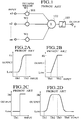
- a neural network circuit generally comprises a multiplicity of neuron circuits connected together, where each neuron circuit is a circuit with a plurality of inputs (x1, x2, ⁇ , xn) and one output (y) as shown in Fig. 1.
- each neuron circuit is a circuit with a plurality of inputs (x1, x2, ⁇ , xn) and one output (y) as shown in Fig. 1.
- Fig. 1 In this neuron circuit of Fig.
- each synapse calculation circuit 101 carries out a calculation for obtaining a product of each input value and each synapse weight value, an absolute value of a difference between each input value and each synapse weight value, or a square of a difference between each input value and each synapse weight value, etc., while a summation circuit 102 sums calculation results obtained by all the synapse calculation units 101, and then a nonlinear unit 103 determines an output value according to a size of a summation result obtained by the summation circuit 102.
- the nonlinear unit 103 which finally determines the output value has one of transfer characteristics as shown in Figs. 2A to 2D.
- the sigmoid function form of Fig. 2A has the most general applicability, but it is also possible to use the simplified forms such as a polygonal line form as shown in Fig. 2B or a step function form as shown in Fig. 2C for the purpose of simplifying the calculations, or a non-monotonic form as shown in Fig. 2D for the purpose of improving the functionality of the neural network circuit.
- symbols Th, Th1, Th2, Th3, and Th4 indicate saturation region boundary values in the respective figures which separate the saturation regions in which the output is constant at either Hi or Low level and transient regions in which the output changes according to the input.
- the specific structure of the neural network circuit is determined by the connections of such neuron circuits.
- the most generally used structure is a triple layer structure shown in Fig. 3, which comprises an input layer formed by a plurality of input terminals x1 to xn, a hidden layer formed by a plurality of neuron circuits 111, and an output layer formed by a plurality of neuron circuits 112.
- the signal entered from the input terminals x1 to xn are entered into all the neuron circuits 111 of the hidden layer in parallel and processed in parallel, while the outputs of all the neuron circuits 111 of the hidden layer are entered into all the neuron circuits 112 of the output layer in parallel and processed in parallel.
- the specific neuron circuits react to the entered input signal and realize the processing such as that of the recognition.
- the scale of the realizable neural network circuit can be enlarged by increasing a number of RAMs 122, and the calculation algorithm can be changed easily by changing the program installed on the micro-processor 121.
- the processing speed is restricted by the access speed with respect to the synapse weights in the RAMs 122.
- the amount of calculations for the synapse calculations and the summation increases as the scale of the neural network circuit becomes larger, and this in turn restricts the processing speed for the following reason. Namely, in this conventional configuration, the synapse calculations with respect to all bits of the input value and all bits of the synapse weight for all synapse connections as well as the summation of all the synapse calculation results must be carried out, so that the amount of calculations can be quite enormous and the accesses to the synapse weights in the RAMs 122 associated with these calculations can also take considerable amount of time.
- a neural network circuit receiving a plurality of input values and outputting one output value, comprising: calculation means for carrying out a synapse calculation for each input value and a corresponding synapse weight of each input value which are expressed by binary bit sequences, by using a sequentially specified bit of the corresponding synapse weight, and a summation calculation for sequentially summing synapse calculation results for the input values to obtain a summation value; synapse weight memory circuit for storing a plurality of synapse weights; memory read out circuit for selectively reading out a specified bit of a specified synapse weight from the synapse weight memory circuit to the calculation means; a nonlinear unit for applying a prescribed nonlinear processing to the summation value obtained by the calculation means so as to determine the output value; judging means for judging whether the summation value obtained by the calculation means reached to a saturation region of a transfer characteristic of the nonline
- a neural network system comprising: a plurality of neural network circuits which are independently operating with respect to each other, each neural network circuit receives a plurality of input values and outputs one output value, and includes: calculation means for carrying out a synapse calculation for each input value and a corresponding synapse weight of each input value which are expressed by binary bit sequences, by using all bits of each input value and each one bit of the corresponding synapse weight sequentially specified from upper bits to obtain a partial synapse calculation result for said each one bit and adding each partial synapse calculation result for said each one bit with previous partial synapse calculation results for upper bits of said each one bit, and a summation calculation for sequentially summing synapse calculation results for the input values to obtain a summation value; synapse weight memory circuit for storing a plurality of synapse weights; memory read out circuit for selectively reading out a specified bit of
- a neural network circuit receiving a plurality of input values and outputting one output value, comprising: reference input value register means for storing a plurality of reference input values in correspondence to said plurality of input values; subtractor means for calculating a difference between each input value and a corresponding one of said plurality of reference input values to obtain an input difference for each input value; calculation means for carrying out a synapse calculation for each input difference and a corresponding synapse weight of each input value and a summation calculation for summing synapse calculation results to obtain a summation value; synapse weight memory circuit for storing a plurality of synapse weights; memory read out circuit for selectively reading out the corresponding synapse weight from the synapse weight memory circuit to the calculation means; a nonlinear unit for applying a prescribed nonlinear processing to the summation value obtained by the calculation means so as to determine the output value; coincidence detection means for detecting a
- a processing scheme using a neural network circuit receiving a plurality of input values and outputting one output value, comprising the steps of: (a) carrying out a synapse calculation for each input value and a corresponding synapse weight of each input value which are expressed by binary bit sequences, by using a sequentially specified bit of the corresponding synapse weight, and a summation calculation for sequentially summing synapse calculation results for the input values to obtain a summation value; (b) applying a prescribed nonlinear processing to the summation value obtained at the step (a) so as to determine the output value; (c) judging whether the summation value obtained at the step (a) reached to a saturation region of a transfer characteristic of the prescribed nonlinear processing applied at the step (b); and (d) controlling the step (a) to sequentially carry out the synapse calculation from upper bits of the corresponding synapse weight, and to stop the synapse
- a processing scheme using a neural network system comprising the steps of: (a) independently operating a plurality of neural network circuits with respect to each other, by operating each neural network circuit which receives a plurality of input values and outputs one output value by the steps of: (a1) carrying out a synapse calculation for each input value and a corresponding synapse weight of each input value which are expressed by binary bit sequences, by using all bits of each input value and each one bit of the corresponding synapse weight sequentially specified from upper bits to obtain a partial synapse calculation result for said each one bit and adding each partial synapse calculation result for said each one bit with previous partial synapse calculation results for upper bits of said each one bit, and a summation calculation for sequentially summing synapse calculation results for the input values to obtain a summation value; (a2) applying a prescribed nonlinear processing to the summation value obtained at the step (a1) so as
- a processing scheme using a neural network circuit receiving a plurality of input values and outputting one output value, comprising the steps of: (a) storing in advance a plurality of reference input values in correspondence to said plurality of input values; (b) calculating a difference between each input value and a corresponding one of said plurality of reference input values to obtain an input difference for each input value; (c) carrying out a synapse calculation for each input difference and a corresponding synapse weight of each input value and a summation calculation for summing synapse calculation results to obtain a summation value; (d) applying a prescribed nonlinear processing to the summation value obtained at the step (c) so as to determine the output value; (e) detecting a coincidence of each input value and the corresponding one of said plurality of reference input values; (f) storing in advance a reference output value corresponding to said plurality of reference input values; (g) selectively outputting one of the output value
- Fig. 1 is a schematic diagram of a conventional neuron circuit for a conventional neural network circuit.
- Figs. 2A to 2D are graphs showing typical transfer characteristics of a nonlinear unit used in a neuron circuit of a neural network circuit.
- Fig. 3 is a schematic diagram of a triple layer structure for a neural network circuit.
- Fig. 4 is a schematic diagram of a conventional circuit configuration for realizing a large scale neural network circuit.
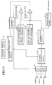
- Fig. 5 is a block diagram of a neuron circuit for the first embodiment of a neural network circuit and a processing scheme according to the present invention.
- Fig. 6 is a diagrammatic illustration of an exemplary calculation for obtaining an initial value of a summation value in the neuron circuit of Fig. 5.
- Fig. 7 is a graph of a transfer characteristic of a nonlinear unit in the neuron circuit of Fig. 5, showing a manner of obtaining a final summation value in one saturation region by the neuron circuit of Fig. 5.
- Fig. 8 is a graph of a transfer characteristic of a nonlinear unit in the neuron circuit of Fig. 5, showing a manner of obtaining a final summation value in another saturation region by the neuron circuit of Fig. 5.
- Fig. 9 is a block diagram of a neuron circuit for the second embodiment of a neural network circuit and a processing scheme according to the present invention.
- Fig. 10 is a block diagram of a neuron circuit for the third embodiment of a neural network circuit and a processing scheme according to the present invention.
- Fig. 11 is a block diagram of a one bit serial synapse calculation and summation circuit in the neuron circuit of Fig. 10.
- Fig. 12 is a diagrammatic illustration of an exemplary calculation in the one bit serial synapse calculation and summation circuit of Fig. 11.
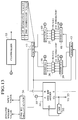
- Fig. 13 is a block diagram of a one bit serial synapse calculation and summation circuit in a neuron circuit for the fourth embodiment of a neural network circuit and a processing scheme according to the present invention.
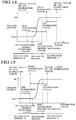
- Fig. 14 is a graph of a transfer characteristic of a nonlinear unit in the neuron circuit of the fourth embodiment, showing a manner of obtaining a final summation value in one saturation region by the fourth embodiment.
- Fig. 15 is a graph of a transfer characteristic of a nonlinear unit in the neuron circuit of the fourth embodiment, showing a manner of obtaining a final summation value in another saturation region by the fourth embodiment.
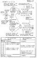
- Fig. 16 is a diagrammatic illustration of an exemplary calculation for obtaining initial values of first and second summation values in the fourth embodiment for one case.
- Fig. 17 is a diagrammatic illustration of an exemplary calculation for obtaining initial values of first and second summation values in the fourth embodiment for another case.
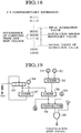
- Fig. 18 is a diagrammatic illustration of an exemplary setting of an initial value of a summation value in a neuron circuit for the fifth embodiment of a neural network circuit and a processing scheme according to the present invention.
- Fig. 19 is a block diagram of a partial configuration for a controller in a one bit serial synapse calculation and summation circuit of a neuron circuit for the fifth embodiment.
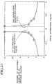
- Fig. 20 is a graph of a rate of executed calculations versus a final summation value showing the effect of the omission of calculations in the first to sixth embodiments of a neural network circuit and a processing scheme according to the present invention.
- Fig. 21 is a graph of a number of accessed upper bits in synapse weight versus a final summation value showing the effect of the reduction of memory accesses in the first to sixth embodiments of a neural network circuit and a processing scheme according to the present invention.
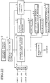
- Fig. 22 is a block diagram of a neuron circuit for the seventh embodiment of a neural network circuit and a processing scheme according to the present invention.
- Fig. 23 is a block diagram of a synapse calculation and summation circuit in the neuron circuit of Fig. 22.
- Fig. 24 is a diagrammatic illustration of an exemplary calculation in the synapse calculation and summation circuit of Fig. 23.
- Fig. 25 is a diagrammatic illustration of an exemplary calculation for obtaining initial values of summation values in the neuron circuit of Fig. 22 for one case.
- Fig. 26 is a diagrammatic illustration of an exemplary calculation for obtaining initial values of summation values in the neuron circuit of Fig. 22 for another case.
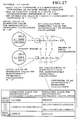
- Fig. 27 is a diagrammatic illustration of an exemplary calculation for obtaining initial values of summation values in the neuron circuit of Fig. 22 for another case.
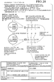
- Fig. 28 is a diagrammatic illustration of an exemplary calculation for obtaining initial values of summation values in the neuron circuit of Fig. 22 for another case.
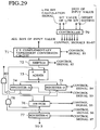
- Fig. 29 is a block diagram of a synapse calculation and summation circuit in a neuron circuit for the eighth embodiment of a neural network circuit and a processing scheme according to the present invention.
- Figs. 30A, 30B, and 30C are graphs of a transfer characteristic of a nonlinear unit in the neuron circuit of the eighth embodiment, showing a manner of providing offsets in the eighth embodiment.
- Fig. 31 is a block diagram of a neural network system using the ninth embodiment of a neural network circuit and a processing scheme according to the present invention.
- Fig. 32 is a timing chart showing an exemplary progress of calculations at neural network circuits in the neural network system of Fig. 31.
- Fig. 33 is a graph of a rate of executed calculations versus a final summation value showing the effect of the omission of calculations in the seventh to ninth embodiments of a neural network circuit and a processing scheme according to the present invention.
- Fig. 34 is a graph of a number of accessed upper bits in synapse weight versus a final summation value showing the effect of the reduction of memory accesses in the seventh to ninth embodiments of a neural network circuit and a processing scheme according to the present invention.
- Fig. 35 is a block diagram of a neuron circuit for the tenth embodiment of a neural network circuit and a processing scheme according to the present invention.
- Fig. 36 is a block diagram of a summation circuit in the neuron circuit of Fig. 35.
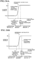
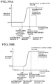
- Figs. 37A and 37B are graphs of a transfer characteristic of a nonlinear unit in the neuron circuit of Fig. 35, showing a manner of determining an omission of calculation in the tenth embodiment for one case.
- Figs. 38A and 38B are graphs of a transfer characteristic of a nonlinear unit in the neuron circuit of Fig. 35, showing a manner of determining an omission of calculation in the tenth embodiment for another case.
- Figs. 39A and 39B are graphs of a transfer characteristic of a nonlinear unit in the neuron circuit of Fig. 35, showing a manner of determining an omission of calculation in the tenth embodiment for another case.
- Fig. 40 is a graph of a rate of executed calculations versus a final summation value showing the effect of the omission of calculations in the tenth embodiment of a neural network circuit and a processing scheme according to the present invention.
- Fig. 41 is a graph of a number of accessed upper bits in synapse weight versus a final summation value showing the effect of the reduction of memory accesses in the tenth embodiment of a neural network circuit and a processing scheme according to the present invention.
- Figs. 5 to 8 the first embodiment of a neural network circuit and a processing scheme using the neural network circuit according to the present invention will be described in detail.
- the neural network circuit has an overall structure similar to the conventional neural network circuit which generally comprises a multiplicity of neuron circuits connected together, as in the triple layer structure of Fig. 3 described above for example.
- each neuron circuit has a configuration as shown in Fig.
- synapse calculation circuits 1-1 to 1-n in correspondence to input 1 to input n for making synapse calculations with respect to the respective inputs; a synapse weight memory circuit 2 for storing synapse weights to be supplied to the synapse calculation circuits 1-1 to 1-n; a memory read out circuit 3 for reading out the synapse weights from the synapse weight memory circuit 2 to the synapse calculation units 1-1 to 1-n; a summation circuit 4 for summing outputs of all the synapse calculation circuits 1-1 to 1-n; a nonlinear unit 5 for carrying out a nonlinear processing with respect to an output of the summation circuit 4 to obtain an output of this neuron circuit; first and second saturation region boundary value registers 8-1 and 8-2 for storing first and second saturation region boundary values of the nonlinear unit 5, respectively; comparators 6-1 and 6-2 for comparing the output of the summation circuit 4 with the first and
- the first and second saturation region boundary values indicate boundaries of a transient region and the saturation regions in a transfer characteristic of the nonlinear unit 5, where the first saturation region boundary value indicates the lower boundary while the second saturation region boundary value indicates the upper boundary.
- the transfer characteristic of the nonlinear unit 5 has more than one transient regions as in a case of Fig. 2D described above, additional saturation region boundary value registers and corresponding comparators will be necessary. In the following, for the sake of simplicity, only a case of the nonlinear unit 5 with the transfer characteristic having one transient region alone will be described.
- synapse calculation circuits 1-1 to 1-n which are connected with corresponding input terminals entering input 1 to input n, as well as with the synapse weight memory circuit 2 through the memory read out circuit 3.
- Outputs of the synapse calculation circuits 1-1 to 1-n are connected to an input of the summation circuit 4, and an output of the summation circuit 4 is connected to inputs of the nonlinear unit 5 and the comparators 6-1 and 6-2, while an output of the nonlinear unit 5 is connected to an output terminal of this neuron circuit.
- the first saturation region boundary value register 8-1 is connected to another input of the comparator 6-1 while the second saturation region boundary value register 8-2 is connected to another input of the comparator 6-2.
- Outputs of the comparators 6-1 and 6-2 are connected to an input of the control circuit 7, while an output of the control circuit 7 is connected to the memory read out circuit 3 and the synapse calculation circuits 1-1 to 1-n.
- each of the input value and the synapse weight value takes either a positive or negative value, so that in a case of carrying out the multiplication of the input value and the synapse weight value as the synapse calculation, it is impossible to realize the monotonously increasing or decreasing function as the summation result by using the conventional synapse calculation and summation scheme. For this reason, in this first embodiment, the following calculation scheme is used.
- the summation gradually converges from the initial value of the summation value to the final value as the calculation progresses.
- the calculation of the synapse calculation result to be summed proceeds from the upper bits, so that the the synapse calculation result changes from that with a larger absolute value to that with a smaller absolute value as the calculation progresses.
- the summation value gradually approaches from the approximated value to the accurate value. Then, when the summation value exceeds the second saturation region boundary value, it can be ascertained that the summation result has reached the saturation region A, so that the subsequent calculations can be omitted.
- Fig. 9 the second embodiment of a neural network circuit and a processing scheme using the neural network circuit according to the present invention will be described in detail.
- those elements which are substantially similar to the corresponding elements in the first embodiment described above will be given the same reference numerals in the figure and their description will be omitted.
- each neuron circuit of the neural network circuit has a configuration as shown in Fig. 9, which differs from that of Fig. 5 in that there is only one synapse calculation circuit 1, and there is provided a selector 9 which is provided between the input terminals and the synapse calculation circuit 1 and controlled by the control circuit 7, such that the synapse weight and the input value to be used in the synapse calculation at the synapse calculation unit 1 are selectively supplied from the memory read out circuit 3 and the selector 9 under the control of the control circuit 7.
- a single synapse calculation circuit 1 is used for all the synapse calculations, so that there is an additional advantage of the reduction of the circuit scale, in addition to all the advantages of the first embodiment described above.
- Figs. 10 to 12 the third embodiment of a neural network circuit and a processing scheme using the neural network circuit according to the present invention will be described in detail.
- those elements which are substantially similar to the corresponding elements in the first and second embodiments described above will be given the same reference numerals in the figure and their description will be omitted.
- each neuron circuit of the neural network circuit has a configuration as shown in Fig. 10, which differs from that of Fig. 9 in that the synapse calculation circuit 1 and the summation circuit 4 of Fig. 9 is replaced by a one bit serial synapse calculation and summation circuit 10, and there is provided a clock generation circuit 11 between the control circuit 7 and this one bit serial synapse calculation and summation circuit 10.
- the one bit serial synapse calculation and summation circuit 10 receives the synapse weight and the input value from the memory read out circuit 3 and the selector 9 under the control of the control circuit 7, and outputs the calculated summation result of the synapse calculations to the nonlinear unit 5 as well as the comparators 6-1 and 6-2.
- the control circuit 7 also supplies a reset signal to the clock generation circuit 11, and the clock generation circuit 11 supplies the clock signals to the one bit serial synapse calculation and summation circuit 10 according to the reset signal from the control circuit 7.
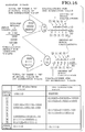
- the one bit serial synapse calculation and summation circuit 10 has a detailed configuration as shown in Fig. 11, which comprises a synapse weight register 21 for registering the received synapse weight, an input value register 22 for registering the received input value, a switch-a 24 and a switch-b 25 for selectively outputting a specified bit of the absolute value bits from the registers 21 and 22, respectively, an EX-OR circuit 28 receiving sign bits of the registers 21 and 22 as its inputs, an AND circuit 30 receiving outputs of the switch-a 24 and the switch-b 25 as its inputs, an EX-OR circuit 29 receiving outputs of the EX-OR circuit 28 and the AND circuit 30 as its inputs, a one bit adder 31 receiving an output of the EX-OR circuit 29 as its A terminal input, a D-type flip flop 32 connected between Co and Ci terminals of the one bit adder 31, a summation register 23 for registering a current summation value, a switch-c 26 for selectively outputting a specified
- the controller 33 supplies a control input i indicating a sequential bit number from the least significant bit of an access bit in the synapse weight register 21 to the switch-a 24, a control input j indicating a sequential bit number from the least significant bit of an access bit in the input value register 22 to the switch-b 25, and a control input k indicating a sequential bit number from the least significant bit of an access bit in the summation register 23 to the switch-c 26 and the switch-d 27, so as to control bits to be selectively outputted or stored by the switches 24, 25, 26, and 27.
- the synapse weight register 21 and the input value register 22 are operated according to the first clock signal CLK1 from the clock generation circuit 11, while the summation register 23 is operated according to the second clock signal CLK2 from the clock generation circuit 11.
- the one bit adder 31 is used for both the addition part of the synapse calculation and the addition part of the summation, so that there is an additional advantage of the reduction of the circuit scale, in addition to all the advantages of the first and second embodiments described above. Moreover, as the serial calculation is carried out, when a bit of the input value is "0", it is apparent that the serial synapse calculation result for that bit is "0", so that the calculation for this bit of the input value and the synapse weight value can be omitted to reduce the amount of calculations.
- the one bit adder 31 can be shared among the addition part of the synapse calculation and the addition part of the summation for the following reason. Namely, in a case of carrying out the serial multiplication as the synapse calculation, as indicated in Fig. 12 for an exemplary case of 11 times 13, the multiplication can be decomposed into the one bit multiplications and the sequential additions of the one bit multiplication results. Consequently, by using such a serial calculation, it is possible to integrally form the addition calculation in the synapse calculation operation and the addition calculation in the summation operation, and thereby there is an additional advantage of the reduction of the circuit scale.
- Figs. 13 to 17 the fourth embodiment of a neural network circuit and a processing scheme using the neural network circuit according to the present invention will be described in detail.
- those elements which are substantially similar to the corresponding elements in the first to third embodiments described above will be given the same reference numerals in the figure and their description will be omitted.
- the initial values for the first and second summation values are set up as follows.
- This initial value of the second summation value has the following significance. Namely, the bit sequences for the partial products between all bits of the absolute value portion of the synapse weight and each bit of the input value are converted into negative values by the 1's complementary expressions. Then, when it is assumed that, among the bit sequences as converted into the 1's complementary expressions, those bit sequences which correspond to the input bit "1" in the input value are entirely composed of "0" except for the most significant bits, a total value of all these bit sequences as converted into the negative values is set as the initial value of the second summation value.
- the one bit multiplication between the synapse weight and the input value is carried out from the upper bits.
- this added bit is subtracted from the first summation value (as in the serial calculations (3), (4), (7), (8), and (9) in Fig. 16, or the serial calculations (1), (2), (5) and (6) in Fig. 17).
- the calculations using the monotonously increasing second summation value for making a judgement for the saturation region A and the calculations using the monotonously decreasing first summation value for making a judgement for the saturation region B can be carried out simultaneously by using the common synapse calculation and summation circuit 10 which operates by sequentially switching the register for registering the first summation value and the register for registering the second summation value.
- the one bit serial synapse calculation and summation circuit of Fig. 13 comprises a one bit multiplicator 34 receiving the synapse weight and the input value specified from the control circuit 7, a switch-g 42 receiving the output of the one bit multiplicator 34 as a control input and supplying the B terminal input of the one bit adder 31, a switch-h 43 receiving the output of the one bit multiplicator 34 as the control input and the S terminal output of the one bit adder 31 as its input, a first summation value register 36 for registering a current first summation value, a switch-c 38 for selectively outputting a specified bit of the current first summation value from the first summation value register 36 as the B terminal input of the one bit adder 31 through the switch-g 42, a switch-d 39 for selectively storing the S terminal output (addition result) of the one bit adder 31 in the first summation value register 36 through the switch-h 43, a second summation value register 37 for registering a current
- the controller 33 supplies a control input k indicating a sequential bit number from the least significant bit of an access bit in the first summation value register 36 or the second summation value register 37 to the switch-c 38 and the switch-d 39 or the switch-e 40 and the switch-f 41, so as to control bits to be selectively outputted or stored by these switches 38, 39, 40, and 41.
- the first summation value register 36 and the second summation value register 37 are operated according to the clock signal CLK2 from the clock generation circuit 11.
- the following processing is carried out.
- (1) The initial values of the first and second summation values are set up as described above.
- (2) The multiplication of the synapse weight and the input value is carried out at the one bit multiplicator 34, and the multiplication result and its sign are obtained.
- the multiplication result and its sign are sent to the control inputs of the switch-g 42 and the switch-h 43 bit by bit, and the switching between the first summation value and the second summation value is carried out according to the following table 1.
- the carry signal and the (k+1)-th bit of the current summation value are added together at the one bit adder 31. This processing is repeated until the carrying of the figure stops occurring, so as to obtain the final summation value.
- the outputs of the first summation value register 36 and the second summation value register 37 are compared with the first and second saturation region boundary values at the comparators 6-1 and 6-2 in the configuration of Fig. 10, so as to make judgements for the saturation regions A and B.
- Figs. 18 and 19 the fifth embodiment of a neural network circuit and a processing scheme using the neural network circuit according to the present invention will be described in detail.
- those elements which are substantially similar to the corresponding elements in the first to fourth embodiments described above will be given the same reference numerals in the figure and their description will be omitted.
- the summation value when the summation value takes a negative value, it is expressed by the 1's complementary expression.
- the initial value of the summation value is set up such that the summation value gradually changes as the summation calculation progresses, and becomes "0" when it has reached the saturation region boundary value, as illustrated in Fig. 18.
- the carry signal from the most significant bit of the summation value is going to be issued, so that the saturation region can be judged and the calculation can be stopped by detecting this carry signal.
- the controller 33 of the one bit serial synapse calculation and summation circuit 10 in the configuration of Fig. 11 or Fig. 13 includes a partial configuration as shown in Fig. 19, which comprises a register 51 for storing a bit length i from the least significant bit of the synapse weight, a register 52 for storing a bit length j from the least significant bit of the input value, a register 53 for registering a variable which is controlled by the carry signal from the summation circuit, a register 54 for registering a constant "1", a register 55 for registering a constant L representing a word length of the absolute value portion of each value, an adder 56 for adding the outputs of the registers 51 and 52, an adder 57 for adding the outputs of the registers 53 and 54 and feeding back the result into the register 53, an adder 58 for adding the outputs of the register 53 and the adder 56 and outputting the control input k of the switches, a comparator 59 for comparing the outputs of the adder
- Fig. 20 shows a relationship between the final summation value and the rate of executed calculations (i.e., a ratio of a number of calculations required in the system of the present invention with respect to a number of calculations required in the system of the prior art) for calculations at one neuron with respect to all the synapse connections in an exemplary case of using 16 inputs where each of the synapse weight and the input value comprises 16 bits including the sign bit and the absolute value portion. It can be seen from this Fig. 20 that the effect of the omission of calculations becomes noticeable for the final summation values which are more distanced from the saturation region boundary values.
- Fig. 21 shows a relationship between the final summation value and the number of accessed upper bits in the synapse weight for the same exemplary case. It can be seen from this Fig. 21 that the effect of the reduction of memory accesses to the synapse weight memory circuit also becomes noticeable for the final summation value which are more distanced from the saturation region boundary values.
- these effects can be estimated quantitatively as follows. First, assuming that a rate by which the input value bit sequences are occupied by "1" bits is 50 %, the omission of calculations for "0" bits in the input value bit sequences amounts to 50 % reduction of the calculations. Moreover, assuming that a possibility for the final summation value to be in the saturation region is 90 %, a possibility for the final summation value to be in the transient region to be 10 %, and the average rate of executed calculations when the final summation value is in the saturation region is 20 % in accordance with Fig. 20, it is possible to reduce the amount of calculations to be approximately 28 %. Consequently, in total, the amount of calculations can be reduced to approximately 14 %.
- a possibility for the final summation value to be in the saturation region is 90 %
- a possibility for the final summation value to be in the transient region is 10 %
- the average number of accessed upper bits in the synapse weight when the final summation value is in the saturation region is 3.2 bits in accordance with Fig. 21, it is possible to reduce the number of memory accesses to be approximately 28 %.
- Figs. 22 to 28 the seventh embodiment of a neural network circuit and a processing scheme using the neural network circuit according to the present invention will be described in detail.
- those elements which are substantially similar to the corresponding elements in the first to sixth embodiments described above will be given the same reference numerals in the figure and their description will be omitted.
- each neuron circuit of the neural network circuit has a configuration as shown in Fig. 22, which differs from that of Fig. 10 for the third embodiment described above in that the one bit serial synapse calculation and summation circuit 10 of Fig. 10 is replaced by a synapse calculation and summation circuit 70.
- This synapse calculation and summation circuit 70 receives the synapse weight and the input value from the memory read out circuit 3 and the selector 9 as well as the clock signals from the clock generation circuit 11 under the control of the control circuit 7, and outputs the calculated summation result of the synapse calculations to the nonlinear unit 5 as well as the comparators 6-1 and 6-2.
- the synapse calculation and summation circuit 70 has a detailed configuration as shown in Fig. 23, which comprises a 2's complementary expression conversion circuit 71 receiving all bits of the input value, a shifter 72 receiving an output of the 2's complementary expression conversion circuit 71, an adder 73 receiving an output of the shifter 72 as its B terminal input, a register-A 74 and a register-B 75 for receiving an S terminal output of the adder 73, a switch 76 receiving outputs of the register-A (register for monotonously increasing summation value) 74 and the register-B (register for monotonously decreasing summation value) 75, a register-C (register for output summation value) 77 for receiving an output of the switch 76 and supplying its output to the nonlinear unit 5, an AND circuit 78 receiving the output of the switch 76 and supplying its output to the adder 73 as an A terminal input, and a controller 79 for supplying control signals S1 to S7 to the 2's complementary expression conversion circuit 71, the shifter
- the controller 79 receives an i-th bit calculation signal indicating that the calculation using the i-th bit is currently executed from the control circuit 7, a bit value of the i-th bit from the least significant bit in the synapse weight from the memory read out circuirt 3, and a sign of the input value from the selector 9.
- the complementary expression can be given by the 2's complementary expression, the 1's complementary expression, etc., but a case of using the 2's complementary expression will be described as an example here. Consequently, the 2's complementary expression in the following description may be replaced by the 1's complementary expression if desired.
- the summation value for the monotonously increasing calculations can make a judgement as to whether it has reached the saturation region A by converging to the final value while monotonously increasing as in Fig. 14, while the summation value for the monotonously decreasing calculations can make a judgement as to whether it has reached the saturation region B by converging to the final value while monotonously decreasing as in Fig. 15. Whenever the summation value has reached to the saturation region A or B, the subsequent calculations are omitted.
- FIG. 29 to 30C the eighth embodiment of a neural network circuit and a processing scheme using the neural network circuit according to the present invention will be described in detail.
- those elements which are substantially similar to the corresponding elements in the seventh embodiment described above will be given the same reference numerals in the figure and their description will be omitted.
- the detailed configuration of the synapse calculation and summation circuit in the seventh embodiment described above is modified such that a judgement as to whether or not the summation value has reached to the saturation region can be made easier.
- the synapse calculation and summation circuit has a detailed configuration as shown in Fig. 29, which differs from that of Fig. 23 in that an additional AND circuit 80 for carrying out the offset processing which receives the most significant bits of the values registered in the register-A 74 and the register-B 75 and outputs the calculation stop signal is provided, and the offset setting as described below is also supplied to the controller 79 from the control circuit 7.
- Figs. 31 and 32 the ninth embodiment of a neural network circuit and a processing scheme using the neural network circuit according to the present invention will be described in detail.
- those elements which are substantially similar to the corresponding elements in the seventh embodiment described above will be given the same reference numerals in the figure and their description will be omitted.
- a neural network system is formed by a plurality of neural network circuits 100-1 to 100-N, where each neural network circuit has a configuration of a neuron circuit similar to that shown in Fig. 22 of the seventh embodiment described above, except that the selector 9 in Fig. 22 is omitted.
- each neuron circuit configuration of each neural network circuit 100 carries out calculations for a plurality of neurons by itself.
- a common input value register 101 for supplying the identical input values to all the neural network circuits 100-1 to 100-N.
- the input values are supplied from the common input value register 101 to the neural network circuits 100-1 to 100-N as follows. Namely, when there are M input values, each input value is transferred to all the neural network circuits 100-1 to 100-N, one by one from the first input value until the M-th input value. When the transfer of the M-th input value is finished, the transfer of these input values are repeated in the similar manner, until all the neural network circuits 100-1 to 100-N finish the calculations.
- all the bits of each input value are transferred together to each neural network circuit 100.
- the synapse calculation using all the bits of the transferred input value and one bit of a corresponding synapse weight is sequentially carried out from the upper bits of the synapse weight, and whenever the summation value reaches to the saturation region, the subsequent calculations are omitted, just as in the seventh embodiment described above.
- each neural network circuit 100 it is possible for each neural network circuit 100 to carry out and stop the calculations, independently from the other neural network circuits 100, in a simple circuit configuration.
- the calculations at the neural network circuits 100-1 to 100-N can progress as shown in Fig. 32 for an exemplary case in which the number of input values M is 3, and each neural network circuit 100 carries out calculations for four neurons.
- the input-1, input-2, and input-3 are sequentially and repeatedly transferred to each neural network circuit 100.
- the synapse calculation using all the bits of the transferred input value and one bit of a corresponding synapse weight is sequentially carried out from the upper bits of the synapse weight, sequentially for each one of the four neurons.
- each neural network circuit 100 Whenever the summation value for one neuron reaches to the saturation region in each neural network circuit 100, the calculations for that neuron is finished by omitting the subsequent calculations and the calculations for a next neuron is started in each neural network circuit 100 independently, so that the calculations at each neural network circuit 100 progresses independently from the progresses of calculations in the other neural network circuits 100.
- Fig. 34 shows a relationship between the final summation value and the number of accessed upper bits in the synapse weight for the same exemplary case. It can be seen from this Fig. 34 that the effect of the reduction of memory accesses to the synapse weight memory circuit also becomes noticeable for the final summation value which are more distanced from the saturation region boundary values.
- these effects can be estimated quantitatively as follows. Namely, assuming that a possibility for the final summation value to be in the saturation region is 90 %, a possibility for the final summation value to be in the transient region to be 10 %, and the average rate of executed calculations when the final summation value is in the saturation region is 20 % in accordance with Fig. 33, it is possible to reduce the amount of calculations to be approximately 28 %.
- Figs. 35 to 41 the tenth embodiment of a neural network circuit and a processing scheme using the neural network circuit according to the present invention will be described in detail.
- those elements which are substantially similar to the corresponding elements in the first to ninth embodiment described above will be given the same reference numerals in the figure and their description will be omitted.
- the synapse calculations for all the synapse connections and the summation for all the neurons are to be carried out by using the input value and the corresponding synapse weight.
- many input signals are to be entered into the neural network continuously, there are cases in which not all of these many input values actually change with respect to each other.
- the input signals corresponding to the background are concerned, they are often given by the identical signals continuously.
- the outputs of the hidden layer are entered into the output layer, but the majority of the hidden layer neurons often have the output levels in the saturation region, so that their outputs often take constant values. In such a case, the majority of the input values for the neurons of the output layer are going to be not changing from each other.
- the utilizable constant values are stored in the memory in advance, and these stored constant values are used as the outputs whenever possible, so as to reduce the amount of calculations as much as possible as well as the number of accesses to the large capacity memory required in conjunction with the calculations.
- each neuron circuit of the neural network circuit has a configuration as shown in Fig. 35, which differs from that of Fig. 9 for the second embodiment described above by further comprising: a plurality of reference input value registers 112 for storing a plurality of reference input values in correspondence to input 1 to input n; a selector 113 for selectively entering one of the reference input values from the reference input value registers 112 under the control of the control circuit 7; a subtractor 114 provided between the selector 9 and the synapse calculation circuit 1 for calculating an input difference between the input value entered from the selector 9 and the reference input value entered from the selector 113, and supplying the calculated input difference to the synapse calculation circuit 1 while also supplying a sign bit of the calculated input difference to the control circuit 7; a coincidence circuit 115 for detecting a coincidence of the input value entered from the selector 9 and the reference input value entered from the selector 113 and supplying a coincidence signal to the control circuit 7;
- the control circuit 7 stops calculations whenever the coincidence signal from the coincidence circuit 115 is received, and controls the switch 119 to output the reference output value from the reference output value register 118.
- the sign data of the synapse weight read out by the memory read out circuit 3 is supplied to the control circuit 7 along with the sign bit of the input difference from the subtractor 114, and the control circuit 7 judges whether it is necessary to carry out the calculation or not according to these sign data and the sign bit as described in detail below, and accordingly controls the switch 119.
- a synapse weight sign memory circuit 116 for separately storing sign data of the synapse weights stored in the synapse weight memory circuit 2, and a sign read out circuit 117 for selectively reading out the sign data of the specified synapse weight to the control circuit 7 under the control of the control circuit 7.
- This configuration is advantageous because the synapse weight memory circuit 2 is going to be a large capacity external memory in a case of a large scale neural network circuit, and it is possible to increase the speed of the processing using the sign data by separately storing the sign data in the synapse weight sign memory circuit 116 which requires only a small capacity just like a cache memory. By means of this, the sign data required in judging whether it is necessary to carry out the calculation or not can be accessed at high speed, without requiring a time consuming access to the large capacity external memory.
- the synapse calculation circuit 1 carries out the synapse calculation with respect to the input difference calculated by the subtractor 114 and the synapse weight corresponding to the input value in the manner similar to that in the first embodiment described above, starting from the upper bits of the binary bit sequences representing the input difference and the synapse weight, such that the subsequent calculations are omitted whenever the comparators 6-1 and 6-2 indicate that the summation value obtained by the summation circuit 4 reaches to the saturation region.
- the summation circuit 4 has a detailed configuration as shown in Fig. 36, which comprises: a summation value register 120 for registering the current summation value to be outputted as an output of the summation circuit 4; a reference summation value register 121 for storing a reference summation value; an initial value setting circuit 122 for setting the initial value of the summation value in a manner described below; a switch 123 for selectively outputting one of the current summation value from the summation value register 120, the reference summation value from the reference summation value register 121, and the initial value from the initial value setting circuit 122; and an adder 124 for adding the output of the switch 123 and the input entered from the synapse calculation circuit 1 and storing the addition result into the summation value register 120.
- the switch 123 is controlled such that the reference summation value from the reference summation value register 121 or the initial value from the initial value setting circuit 122 is outputted at a time of the initial value setting, and the current summation value from the summation value register 120 is outputted at a time of the calculation.
- the initial value of the summation value is set up by the initial value setting circuit 122 as follows, so as to realize the monotonously increasing summation.
- the initial value is set to be the reference summation value from the reference summation value register 121.
- the initial value is obtained by the following steps.
- the synapse calculation is carried out in terms of the binary expressions of the input difference and the synapse weight, bit by bit from the upper bits of their absolute value portions.
- the i-th bit of the input difference is "0”
- the synapse calculation result for that i-th bit is "0”
- the calculation for this i-th bit of the input difference and the synapse weight is omitted.
- the summation gradually converges from the initial value of the summation to the final value as the calculation progresses, and the calculation of the synapse calculation result to be summed proceeds from the upper bits, so that the the synapse calculation result changes from that with a larger absolute value to that with a smaller absolute value as the calculation progresses.
- the summation value gradually approaches from the approximated value to the accurate value. Then, when the summation value exceeds the first or second saturation region boundary value, it can be ascertained that the summation result has reached the saturation region B or A, so that the subsequent calculations can be omitted.
- the reference input values, the reference summation value, and the reference output value may be updated only when the current summation value has changed in a direction of approaching to the saturation region boundary value, so as to set new reference input values, reference summation value, and reference output value for judging the necessity of the subsequent calculations.
- the other manner of updating the reference input values, the reference summation value, and the reference output value may be employed according to the input conditions and the application, if desired
- the reference input values, the reference summation value, and the reference output value are provided in advance, such that the synapse calculation for the input difference is carried out only when the input value differs from the reference input values, and the final summation value is obtained by adding this synapse calculation result with the reference summation value.
- the reference output value is outputted from the reference output value register 118, such that the amount of calculations as well as the number of accesses to the synapse weight memory circuit 2 which are required in conjunction with the synapse calculations can be reduced considerably.
- this processing is carried out according to the situations as follows.
- Fig. 40 shows a relationship between the final summation value and the rate of executed calculations (i.e., a ratio of a number of calculations required in the system of the present invention with respect to a number of calculations required in the system of the prior art) for varying inputs in an exemplary case in which each of the synapse weight, the input value, and the reference input value comprises 16 bits including the sign bit and the absolute value portion, the reference summation value is set to be -0.693, the synapse weight is set to be -0.599, the reference input value is set to be 1.0, the first saturation region boundary value is set to be -0.5, and the second saturation region boundary value is set to be 0.5. It can be seen from this Fig. 40 that the effect of the omission of calculations becomes noticeable for the final summation values which are more distanced from the saturation region boundary values.
- Fig. 41 shows a relationship between the final summation value and the number of accessed upper bits in the synapse weight for the same exemplary case. It can be seen from this Fig. 41 that the effect of the reduction of memory accesses to the synapse weight memory circuit also becomes noticeable for the final summation value which are more distanced from the saturation region boundary values.
- a possibility for the reference summation value to be in the saturation region is 90 %
- a possibility for the reference summation value to be in the transient region is 10 %
- a possibility for the summation value to change in a direction approaching to the saturation region boundary value when the reference summation value is in the saturation region is 50 %
- a possibility for the summation value to change in a direction departing from the saturation region boundary value when the reference summation value is in the saturation region is 50 %
- a possibility for the final summation value to be in the saturation region when the summation value approaches to the saturation region boundary value is 90 %
- a possibility for the final summation value to be in the transient region when the summation value approaches to the saturation region boundary value is 10 %
- the average rate of executed calculations when the final summation value is in the saturation region is 20 % in accordance with Fig. 40
Landscapes
- Engineering & Computer Science (AREA)
- Physics & Mathematics (AREA)
- Theoretical Computer Science (AREA)
- Health & Medical Sciences (AREA)
- Life Sciences & Earth Sciences (AREA)
- Biomedical Technology (AREA)
- Biophysics (AREA)
- General Health & Medical Sciences (AREA)
- Data Mining & Analysis (AREA)
- Evolutionary Computation (AREA)
- Computational Linguistics (AREA)
- Molecular Biology (AREA)
- Computing Systems (AREA)
- General Engineering & Computer Science (AREA)
- General Physics & Mathematics (AREA)
- Mathematical Physics (AREA)
- Software Systems (AREA)
- Artificial Intelligence (AREA)
- Neurology (AREA)
- Complex Calculations (AREA)
Priority Applications (1)
| Application Number | Priority Date | Filing Date | Title |
|---|---|---|---|
| EP00113124A EP1033660A1 (de) | 1994-01-19 | 1995-01-18 | Neuronal-Netzwerksverarbeitungsverfahren und -Anlage mit reduzierter Berechnungsmenge |
Applications Claiming Priority (9)
| Application Number | Priority Date | Filing Date | Title |
|---|---|---|---|
| JP6003885A JPH07210617A (ja) | 1994-01-19 | 1994-01-19 | ニューラルネットワーク回路および本回路を用いた演算方法 |
| JP3885/94 | 1994-01-19 | ||
| JP6004043A JPH07210533A (ja) | 1994-01-19 | 1994-01-19 | ニューラルネットワーク回路及びこれを用いた演算方法 |
| JP388594 | 1994-01-19 | ||
| JP404394 | 1994-01-19 | ||
| JP4043/94 | 1994-01-19 | ||
| JP16564194 | 1994-07-18 | ||
| JP6165641A JPH0830572A (ja) | 1994-07-18 | 1994-07-18 | ニューラルネットワーク回路及びこれを用いた演算方法 |
| JP165641/94 | 1994-07-18 |
Related Child Applications (1)
| Application Number | Title | Priority Date | Filing Date |
|---|---|---|---|
| EP00113124A Division EP1033660A1 (de) | 1994-01-19 | 1995-01-18 | Neuronal-Netzwerksverarbeitungsverfahren und -Anlage mit reduzierter Berechnungsmenge |
Publications (3)
| Publication Number | Publication Date |
|---|---|
| EP0664516A2 true EP0664516A2 (de) | 1995-07-26 |
| EP0664516A3 EP0664516A3 (de) | 1995-12-20 |
| EP0664516B1 EP0664516B1 (de) | 2003-08-06 |
Family
ID=27276023
Family Applications (2)
| Application Number | Title | Priority Date | Filing Date |
|---|---|---|---|
| EP00113124A Withdrawn EP1033660A1 (de) | 1994-01-19 | 1995-01-18 | Neuronal-Netzwerksverarbeitungsverfahren und -Anlage mit reduzierter Berechnungsmenge |
| EP95100620A Expired - Lifetime EP0664516B1 (de) | 1994-01-19 | 1995-01-18 | Neuronales netzwerk mit reduzierter Berechnungsmenge |
Family Applications Before (1)
| Application Number | Title | Priority Date | Filing Date |
|---|---|---|---|
| EP00113124A Withdrawn EP1033660A1 (de) | 1994-01-19 | 1995-01-18 | Neuronal-Netzwerksverarbeitungsverfahren und -Anlage mit reduzierter Berechnungsmenge |
Country Status (4)
| Country | Link |
|---|---|
| US (1) | US5630024A (de) |
| EP (2) | EP1033660A1 (de) |
| KR (1) | KR0168975B1 (de) |
| DE (1) | DE69531418T2 (de) |
Cited By (8)
| Publication number | Priority date | Publication date | Assignee | Title |
|---|---|---|---|---|
| EP0814636A1 (de) * | 1996-06-21 | 1997-12-29 | Siemens Audiologische Technik GmbH | Hörgerät |
| EP1014274A4 (de) * | 1998-06-16 | 2003-10-08 | Joint Stock Company Res Ct Mod | Neuronaler Prozessor, Vorrichtung zur Berechnung von Sättigungsfunktionen |
| CN106056212A (zh) * | 2016-05-25 | 2016-10-26 | 清华大学 | 一种人工神经网络计算核 |
| CN108345935A (zh) * | 2017-01-25 | 2018-07-31 | 株式会社东芝 | 积和运算器、网络单元及网络装置 |
| EP3617960A1 (de) * | 2018-09-03 | 2020-03-04 | Samsung Electronics Co., Ltd. | Neuromorphes verfahren und vorrichtung mit neuromorphem multibit-betrieb |
| US20200074284A1 (en) * | 2018-09-03 | 2020-03-05 | Samsung Electronics Co., Ltd. | Two-dimensional array-based neuromorphic processor and implementing method |
| KR20200094534A (ko) * | 2019-01-30 | 2020-08-07 | 삼성전자주식회사 | 뉴럴 네트워크 장치 및 뉴럴 네트워크 장치에서 멀티-비트 연산을 처리하는 방법 |
| JP2021144727A (ja) * | 2016-05-26 | 2021-09-24 | タータン エーアイ リミテッド | ディープニューラルネットワークについての加速器 |
Families Citing this family (13)
| Publication number | Priority date | Publication date | Assignee | Title |
|---|---|---|---|---|
| FI20002853L (fi) | 2000-12-22 | 2002-06-23 | Nokia Corp | Keinotekoisen assosiatiivisen neuronin synapsi |
| US20150278680A1 (en) * | 2014-03-26 | 2015-10-01 | Qualcomm Incorporated | Training, recognition, and generation in a spiking deep belief network (dbn) |
| US20150286925A1 (en) * | 2014-04-08 | 2015-10-08 | Qualcomm Incorporated | Modulating plasticity by global scalar values in a spiking neural network |
| CN110383282A (zh) * | 2017-02-07 | 2019-10-25 | 密执安州立大学董事会 | 用于混合信号计算的系统和方法 |
| JP6865847B2 (ja) * | 2017-04-19 | 2021-04-28 | シャンハイ カンブリコン インフォメーション テクノロジー カンパニー リミテッドShanghai Cambricon Information Technology Co.,Ltd. | 処理装置、チップ、電子設備及び方法 |
| US11256978B2 (en) | 2017-07-14 | 2022-02-22 | Intel Corporation | Hyperbolic functions for machine learning acceleration |
| US11630997B2 (en) | 2018-01-23 | 2023-04-18 | Samsung Electronics Co., Ltd. | Method and apparatus with bit-serial data processing of a neural network |
| KR102833321B1 (ko) * | 2018-12-12 | 2025-07-10 | 삼성전자주식회사 | 뉴럴 네트워크에서 컨볼루션 연산을 수행하는 방법 및 장치 |
| KR102703432B1 (ko) * | 2018-12-31 | 2024-09-06 | 삼성전자주식회사 | 메모리 장치를 이용한 계산 방법 및 이를 수행하는 메모리 장치 |
| KR102878420B1 (ko) * | 2019-09-05 | 2025-10-29 | 에스케이하이닉스 주식회사 | Mac 연산 동작을 수행하는 비휘발성 메모리 장치 |
| KR102716444B1 (ko) * | 2019-09-05 | 2024-10-11 | 에스케이하이닉스 주식회사 | Mac 연산 동작을 수행하는 비휘발성 메모리 장치 |
| KR102838860B1 (ko) | 2019-12-26 | 2025-07-28 | 삼성전자주식회사 | 메모리 장치, 및 이를 포함하는 전자 기기 |
| US12481867B2 (en) * | 2021-04-28 | 2025-11-25 | Arm Limited | Memory for artificial neural network accelerator |
Family Cites Families (16)
| Publication number | Priority date | Publication date | Assignee | Title |
|---|---|---|---|---|
| US4943931A (en) * | 1988-05-02 | 1990-07-24 | Trw Inc. | Digital artificial neural processor |
| DE58906476D1 (de) * | 1988-07-05 | 1994-02-03 | Siemens Ag | In integrierter Schaltungstechnik ausgeführtes digitales neuronales Netz. |
| US5324991A (en) * | 1989-07-12 | 1994-06-28 | Ricoh Company, Ltd. | Neuron unit and neuron unit network |
| US5131073A (en) * | 1989-07-12 | 1992-07-14 | Ricoh Company, Ltd. | Neuron unit and neuron unit network |
| US5481646A (en) * | 1989-07-12 | 1996-01-02 | Ricoh Company, Ltd. | Neuron unit and neuron unit network |
| JP2565791B2 (ja) * | 1990-04-19 | 1996-12-18 | 富士写真フイルム株式会社 | 多層型ニューラルネットワークの係数格納装置 |
| US5166539A (en) * | 1990-07-09 | 1992-11-24 | Nippon Telegraph And Telephone Corporation | Neural network circuit |
| US5208900A (en) * | 1990-10-22 | 1993-05-04 | Motorola, Inc. | Digital neural network computation ring |
| JPH056356A (ja) * | 1990-11-20 | 1993-01-14 | Ricoh Co Ltd | 信号処理方法及びその装置 |
| JP2760170B2 (ja) * | 1990-11-29 | 1998-05-28 | 松下電器産業株式会社 | 学習機械 |
| FR2681709B1 (fr) * | 1991-09-20 | 1993-11-05 | Thomson Csf | Procede de connexion interne pour reseaux de neurones. |
| US5440671A (en) * | 1992-07-30 | 1995-08-08 | Olympus Optical Co., Ltd. | Neural net model and neural net optimizing method and system for realizing the same |
| KR0178805B1 (ko) * | 1992-08-27 | 1999-05-15 | 정호선 | 스스로 학습이 가능한 다층 신경회로망 및 학습 방법 |
| US5350953A (en) * | 1993-05-28 | 1994-09-27 | Swenson Richard M | Digitally weighted neuron for artificial neural network |
| US5473731A (en) * | 1993-07-20 | 1995-12-05 | Intel Corporation | Lattice based dynamic programming classification system |
| US5473730A (en) * | 1993-11-09 | 1995-12-05 | At&T Ipm Corp. | High efficiency learning network |
-
1995
- 1995-01-17 US US08/373,440 patent/US5630024A/en not_active Expired - Fee Related
- 1995-01-18 EP EP00113124A patent/EP1033660A1/de not_active Withdrawn
- 1995-01-18 KR KR1019950000739A patent/KR0168975B1/ko not_active Expired - Fee Related
- 1995-01-18 EP EP95100620A patent/EP0664516B1/de not_active Expired - Lifetime
- 1995-01-18 DE DE69531418T patent/DE69531418T2/de not_active Expired - Fee Related
Cited By (18)
| Publication number | Priority date | Publication date | Assignee | Title |
|---|---|---|---|---|
| EP0814636A1 (de) * | 1996-06-21 | 1997-12-29 | Siemens Audiologische Technik GmbH | Hörgerät |
| US6044163A (en) * | 1996-06-21 | 2000-03-28 | Siemens Audiologische Technik Gmbh | Hearing aid having a digitally constructed calculating unit employing a neural structure |
| EP1014274A4 (de) * | 1998-06-16 | 2003-10-08 | Joint Stock Company Res Ct Mod | Neuronaler Prozessor, Vorrichtung zur Berechnung von Sättigungsfunktionen |
| CN106056212A (zh) * | 2016-05-25 | 2016-10-26 | 清华大学 | 一种人工神经网络计算核 |
| CN106056212B (zh) * | 2016-05-25 | 2018-11-23 | 清华大学 | 一种人工神经网络计算核 |
| JP2021144727A (ja) * | 2016-05-26 | 2021-09-24 | タータン エーアイ リミテッド | ディープニューラルネットワークについての加速器 |
| CN108345935A (zh) * | 2017-01-25 | 2018-07-31 | 株式会社东芝 | 积和运算器、网络单元及网络装置 |
| KR20200026586A (ko) * | 2018-09-03 | 2020-03-11 | 삼성전자주식회사 | 2차원 어레이 기반 뉴로모픽 프로세서 및 그 동작 방법 |
| US20200074284A1 (en) * | 2018-09-03 | 2020-03-05 | Samsung Electronics Co., Ltd. | Two-dimensional array-based neuromorphic processor and implementing method |
| EP3617960A1 (de) * | 2018-09-03 | 2020-03-04 | Samsung Electronics Co., Ltd. | Neuromorphes verfahren und vorrichtung mit neuromorphem multibit-betrieb |
| US11663451B2 (en) * | 2018-09-03 | 2023-05-30 | Samsung Electronics Co., Ltd. | Two-dimensional array-based neuromorphic processor and implementing method |
| US20230214637A1 (en) * | 2018-09-03 | 2023-07-06 | Samsung Electronics Co., Ltd. | Two-dimensional array-based neuromorphic processor and implementing method |
| US11868874B2 (en) | 2018-09-03 | 2024-01-09 | Samsung Electronics Co., Ltd. | Two-dimensional array-based neuromorphic processor and implementing method |
| US11868870B2 (en) | 2018-09-03 | 2024-01-09 | Samsung Electronics Co., Ltd. | Neuromorphic method and apparatus with multi-bit neuromorphic operation |
| KR20200094534A (ko) * | 2019-01-30 | 2020-08-07 | 삼성전자주식회사 | 뉴럴 네트워크 장치 및 뉴럴 네트워크 장치에서 멀티-비트 연산을 처리하는 방법 |
| US11531870B2 (en) * | 2019-01-30 | 2022-12-20 | Samsung Electronics Co., Ltd. | Neural network apparatus and method of processing variable-resolution operation by the same |
| US20230076169A1 (en) * | 2019-01-30 | 2023-03-09 | Samsung Electronics Co., Ltd. | Neural network apparatus and method of processing variable-resolution operation by the same |
| US11853869B2 (en) * | 2019-01-30 | 2023-12-26 | Samsung Electronics Co., Ltd. | Neural network apparatus and method of processing variable-resolution operation by the same |
Also Published As
| Publication number | Publication date |
|---|---|
| EP0664516A3 (de) | 1995-12-20 |
| US5630024A (en) | 1997-05-13 |
| EP0664516B1 (de) | 2003-08-06 |
| KR0168975B1 (ko) | 1999-01-15 |
| EP1033660A1 (de) | 2000-09-06 |
| DE69531418T2 (de) | 2004-07-08 |
| DE69531418D1 (de) | 2003-09-11 |
| KR950024084A (ko) | 1995-08-21 |
Similar Documents
| Publication | Publication Date | Title |
|---|---|---|
| EP0664516A2 (de) | Neuronales netzwerk mit reduzierter Berechnungsmenge | |
| Namin et al. | Efficient hardware implementation of the hyperbolic tangent sigmoid function | |
| US6151594A (en) | Artificial neuron and method of using same | |
| EP0182963B1 (de) | Addierer für Gleitkommadaten | |
| CA1244955A (en) | Processing circuit capable of raising throughput of accumulation | |
| US4412208A (en) | Digital to analog converter | |
| EP0209049A2 (de) | Verarbeitungsschaltung, fähig zum Erhöhen des Akkumulationsdurchsatzes | |
| JPH08297716A (ja) | ニューラル・ネットワーク用の適応型重み調整回路 | |
| KR950001601B1 (ko) | 뉴-럴 네트워크 회로 | |
| EP0214831B1 (de) | Analog/Digital-Wandler und Verfahren zur Analog/Digital Wandlung | |
| CN118780368B (zh) | 动态旁路选择的多模态网络加速方法及系统 | |
| US6411241B1 (en) | A/D converter | |
| US5455583A (en) | Combined conventional/neural network analog to digital converter | |
| US4763108A (en) | Digital-to-analog conversion system | |
| US4891782A (en) | Parallel neural network for a full binary adder | |
| US6304203B1 (en) | Successive approximation AD converter and microcomputer incorporating the same | |
| JPH07210533A (ja) | ニューラルネットワーク回路及びこれを用いた演算方法 | |
| JPH09128241A (ja) | ファジーロジックプロセッサの言語入力値の所属関数値に対する配列方法および装置 | |
| JPH09101944A (ja) | ニューラルネットワーク回路 | |
| US5502401A (en) | Controllable width or gate | |
| CN114168192B (zh) | 一种数据位数转换电路及方法 | |
| CN112596698A (zh) | 一种基于多比特近似加法器的双电压动态配置硬件电路结构 | |
| US6516333B1 (en) | Sticky bit value predicting circuit | |
| CN118199633B (zh) | 面向时间交织模数转换器的杂散自修复多模态运算电路 | |
| EP0661646A2 (de) | Neuronalschaltung |
Legal Events
| Date | Code | Title | Description |
|---|---|---|---|
| PUAI | Public reference made under article 153(3) epc to a published international application that has entered the european phase |
Free format text: ORIGINAL CODE: 0009012 |
|
| 17P | Request for examination filed |
Effective date: 19950118 |
|
| AK | Designated contracting states |
Kind code of ref document: A2 Designated state(s): DE FR GB |
|
| PUAL | Search report despatched |
Free format text: ORIGINAL CODE: 0009013 |
|
| AK | Designated contracting states |
Kind code of ref document: A3 Designated state(s): DE FR GB |
|
| RAP1 | Party data changed (applicant data changed or rights of an application transferred) |
Owner name: NIPPON TELEGRAPH AND TELEPHONE CORPORATION |
|
| 17Q | First examination report despatched |
Effective date: 20000217 |
|
| GRAH | Despatch of communication of intention to grant a patent |
Free format text: ORIGINAL CODE: EPIDOS IGRA |
|
| GRAH | Despatch of communication of intention to grant a patent |
Free format text: ORIGINAL CODE: EPIDOS IGRA |
|
| GRAA | (expected) grant |
Free format text: ORIGINAL CODE: 0009210 |
|
| AK | Designated contracting states |
Designated state(s): DE FR GB |
|
| REG | Reference to a national code |
Ref country code: GB Ref legal event code: FG4D |
|
| REF | Corresponds to: |
Ref document number: 69531418 Country of ref document: DE Date of ref document: 20030911 Kind code of ref document: P |
|
| ET | Fr: translation filed | ||
| PLBE | No opposition filed within time limit |
Free format text: ORIGINAL CODE: 0009261 |
|
| STAA | Information on the status of an ep patent application or granted ep patent |
Free format text: STATUS: NO OPPOSITION FILED WITHIN TIME LIMIT |
|
| 26N | No opposition filed |
Effective date: 20040507 |
|
| PGFP | Annual fee paid to national office [announced via postgrant information from national office to epo] |
Ref country code: FR Payment date: 20041216 Year of fee payment: 11 |
|
| PGFP | Annual fee paid to national office [announced via postgrant information from national office to epo] |
Ref country code: GB Payment date: 20041229 Year of fee payment: 11 |
|
| PGFP | Annual fee paid to national office [announced via postgrant information from national office to epo] |
Ref country code: DE Payment date: 20050126 Year of fee payment: 11 |
|
| PG25 | Lapsed in a contracting state [announced via postgrant information from national office to epo] |
Ref country code: GB Free format text: LAPSE BECAUSE OF NON-PAYMENT OF DUE FEES Effective date: 20060118 |
|
| PG25 | Lapsed in a contracting state [announced via postgrant information from national office to epo] |
Ref country code: FR Free format text: LAPSE BECAUSE OF NON-PAYMENT OF DUE FEES Effective date: 20060131 |
|
| PG25 | Lapsed in a contracting state [announced via postgrant information from national office to epo] |
Ref country code: DE Free format text: LAPSE BECAUSE OF NON-PAYMENT OF DUE FEES Effective date: 20060801 |
|
| GBPC | Gb: european patent ceased through non-payment of renewal fee |
Effective date: 20060118 |
|
| REG | Reference to a national code |
Ref country code: FR Ref legal event code: ST Effective date: 20060929 |