EP0664576A2 - Module avec broches de contact - Google Patents
Module avec broches de contact Download PDFInfo
- Publication number
- EP0664576A2 EP0664576A2 EP94118583A EP94118583A EP0664576A2 EP 0664576 A2 EP0664576 A2 EP 0664576A2 EP 94118583 A EP94118583 A EP 94118583A EP 94118583 A EP94118583 A EP 94118583A EP 0664576 A2 EP0664576 A2 EP 0664576A2
- Authority
- EP
- European Patent Office
- Prior art keywords
- pin
- substrate
- compliant
- pins
- circuit board
- Prior art date
- Legal status (The legal status is an assumption and is not a legal conclusion. Google has not performed a legal analysis and makes no representation as to the accuracy of the status listed.)
- Withdrawn
Links
Images



Classifications
-
- H—ELECTRICITY
- H05—ELECTRIC TECHNIQUES NOT OTHERWISE PROVIDED FOR
- H05K—PRINTED CIRCUITS; CASINGS OR CONSTRUCTIONAL DETAILS OF ELECTRIC APPARATUS; MANUFACTURE OF ASSEMBLAGES OF ELECTRICAL COMPONENTS
- H05K1/00—Printed circuits
- H05K1/02—Details
- H05K1/14—Structural association of two or more printed circuits
-
- H—ELECTRICITY
- H01—ELECTRIC ELEMENTS
- H01R—ELECTRICALLY-CONDUCTIVE CONNECTIONS; STRUCTURAL ASSOCIATIONS OF A PLURALITY OF MUTUALLY-INSULATED ELECTRICAL CONNECTING ELEMENTS; COUPLING DEVICES; CURRENT COLLECTORS
- H01R12/00—Structural associations of a plurality of mutually-insulated electrical connecting elements, specially adapted for printed circuits, e.g. printed circuit boards [PCB], flat or ribbon cables, or like generally planar structures, e.g. terminal strips, terminal blocks; Coupling devices specially adapted for printed circuits, flat or ribbon cables, or like generally planar structures; Terminals specially adapted for contact with, or insertion into, printed circuits, flat or ribbon cables, or like generally planar structures
- H01R12/50—Fixed connections
- H01R12/51—Fixed connections for rigid printed circuits or like structures
- H01R12/55—Fixed connections for rigid printed circuits or like structures characterised by the terminals
- H01R12/58—Fixed connections for rigid printed circuits or like structures characterised by the terminals terminals for insertion into holes
-
- H—ELECTRICITY
- H01—ELECTRIC ELEMENTS
- H01R—ELECTRICALLY-CONDUCTIVE CONNECTIONS; STRUCTURAL ASSOCIATIONS OF A PLURALITY OF MUTUALLY-INSULATED ELECTRICAL CONNECTING ELEMENTS; COUPLING DEVICES; CURRENT COLLECTORS
- H01R12/00—Structural associations of a plurality of mutually-insulated electrical connecting elements, specially adapted for printed circuits, e.g. printed circuit boards [PCB], flat or ribbon cables, or like generally planar structures, e.g. terminal strips, terminal blocks; Coupling devices specially adapted for printed circuits, flat or ribbon cables, or like generally planar structures; Terminals specially adapted for contact with, or insertion into, printed circuits, flat or ribbon cables, or like generally planar structures
- H01R12/50—Fixed connections
- H01R12/51—Fixed connections for rigid printed circuits or like structures
- H01R12/52—Fixed connections for rigid printed circuits or like structures connecting to other rigid printed circuits or like structures
- H01R12/523—Fixed connections for rigid printed circuits or like structures connecting to other rigid printed circuits or like structures by an interconnection through aligned holes in the boards or multilayer board
-
- H—ELECTRICITY
- H05—ELECTRIC TECHNIQUES NOT OTHERWISE PROVIDED FOR
- H05K—PRINTED CIRCUITS; CASINGS OR CONSTRUCTIONAL DETAILS OF ELECTRIC APPARATUS; MANUFACTURE OF ASSEMBLAGES OF ELECTRICAL COMPONENTS
- H05K2201/00—Indexing scheme relating to printed circuits covered by H05K1/00
- H05K2201/04—Assemblies of printed circuits
- H05K2201/042—Stacked spaced PCBs; Planar parts of folded flexible circuits having mounted components in between or spaced from each other
-
- H—ELECTRICITY
- H05—ELECTRIC TECHNIQUES NOT OTHERWISE PROVIDED FOR
- H05K—PRINTED CIRCUITS; CASINGS OR CONSTRUCTIONAL DETAILS OF ELECTRIC APPARATUS; MANUFACTURE OF ASSEMBLAGES OF ELECTRICAL COMPONENTS
- H05K2201/00—Indexing scheme relating to printed circuits covered by H05K1/00
- H05K2201/20—Details of printed circuits not provided for in H05K2201/01 - H05K2201/10
- H05K2201/2036—Permanent spacer or stand-off in a printed circuit or printed circuit assembly
-
- H—ELECTRICITY
- H05—ELECTRIC TECHNIQUES NOT OTHERWISE PROVIDED FOR
- H05K—PRINTED CIRCUITS; CASINGS OR CONSTRUCTIONAL DETAILS OF ELECTRIC APPARATUS; MANUFACTURE OF ASSEMBLAGES OF ELECTRICAL COMPONENTS
- H05K3/00—Apparatus or processes for manufacturing printed circuits
- H05K3/30—Assembling printed circuits with electric components, e.g. with resistors
- H05K3/306—Assembling printed circuits with electric components, e.g. with resistors with lead-in-hole components
- H05K3/308—Adaptations of leads
-
- H—ELECTRICITY
- H05—ELECTRIC TECHNIQUES NOT OTHERWISE PROVIDED FOR
- H05K—PRINTED CIRCUITS; CASINGS OR CONSTRUCTIONAL DETAILS OF ELECTRIC APPARATUS; MANUFACTURE OF ASSEMBLAGES OF ELECTRICAL COMPONENTS
- H05K3/00—Apparatus or processes for manufacturing printed circuits
- H05K3/36—Assembling printed circuits with other printed circuits
- H05K3/368—Assembling printed circuits with other printed circuits parallel to each other
-
- Y—GENERAL TAGGING OF NEW TECHNOLOGICAL DEVELOPMENTS; GENERAL TAGGING OF CROSS-SECTIONAL TECHNOLOGIES SPANNING OVER SEVERAL SECTIONS OF THE IPC; TECHNICAL SUBJECTS COVERED BY FORMER USPC CROSS-REFERENCE ART COLLECTIONS [XRACs] AND DIGESTS
- Y10—TECHNICAL SUBJECTS COVERED BY FORMER USPC
- Y10T—TECHNICAL SUBJECTS COVERED BY FORMER US CLASSIFICATION
- Y10T29/00—Metal working
- Y10T29/49—Method of mechanical manufacture
- Y10T29/49002—Electrical device making
- Y10T29/49117—Conductor or circuit manufacturing
- Y10T29/49124—On flat or curved insulated base, e.g., printed circuit, etc.
- Y10T29/49126—Assembling bases
-
- Y—GENERAL TAGGING OF NEW TECHNOLOGICAL DEVELOPMENTS; GENERAL TAGGING OF CROSS-SECTIONAL TECHNOLOGIES SPANNING OVER SEVERAL SECTIONS OF THE IPC; TECHNICAL SUBJECTS COVERED BY FORMER USPC CROSS-REFERENCE ART COLLECTIONS [XRACs] AND DIGESTS
- Y10—TECHNICAL SUBJECTS COVERED BY FORMER USPC
- Y10T—TECHNICAL SUBJECTS COVERED BY FORMER US CLASSIFICATION
- Y10T29/00—Metal working
- Y10T29/49—Method of mechanical manufacture
- Y10T29/49002—Electrical device making
- Y10T29/49117—Conductor or circuit manufacturing
- Y10T29/49124—On flat or curved insulated base, e.g., printed circuit, etc.
- Y10T29/49147—Assembling terminal to base
- Y10T29/49151—Assembling terminal to base by deforming or shaping
- Y10T29/49153—Assembling terminal to base by deforming or shaping with shaping or forcing terminal into base aperture
-
- Y—GENERAL TAGGING OF NEW TECHNOLOGICAL DEVELOPMENTS; GENERAL TAGGING OF CROSS-SECTIONAL TECHNOLOGIES SPANNING OVER SEVERAL SECTIONS OF THE IPC; TECHNICAL SUBJECTS COVERED BY FORMER USPC CROSS-REFERENCE ART COLLECTIONS [XRACs] AND DIGESTS
- Y10—TECHNICAL SUBJECTS COVERED BY FORMER USPC
- Y10T—TECHNICAL SUBJECTS COVERED BY FORMER US CLASSIFICATION
- Y10T29/00—Metal working
- Y10T29/49—Method of mechanical manufacture
- Y10T29/49002—Electrical device making
- Y10T29/49117—Conductor or circuit manufacturing
- Y10T29/49124—On flat or curved insulated base, e.g., printed circuit, etc.
- Y10T29/49155—Manufacturing circuit on or in base
- Y10T29/49165—Manufacturing circuit on or in base by forming conductive walled aperture in base
-
- Y—GENERAL TAGGING OF NEW TECHNOLOGICAL DEVELOPMENTS; GENERAL TAGGING OF CROSS-SECTIONAL TECHNOLOGIES SPANNING OVER SEVERAL SECTIONS OF THE IPC; TECHNICAL SUBJECTS COVERED BY FORMER USPC CROSS-REFERENCE ART COLLECTIONS [XRACs] AND DIGESTS
- Y10—TECHNICAL SUBJECTS COVERED BY FORMER USPC
- Y10T—TECHNICAL SUBJECTS COVERED BY FORMER US CLASSIFICATION
- Y10T29/00—Metal working
- Y10T29/53—Means to assemble or disassemble
- Y10T29/5313—Means to assemble electrical device
- Y10T29/53174—Means to fasten electrical component to wiring board, base, or substrate
Definitions
- the present invention relates to a novel pinned module and a method for making the same.
- circuit boards and other like devices In the design of complicated electronic components, it is not uncommon to arrange circuit boards and other like devices in stacked relation with numerous electrical connections being made between the different boards. Typically this is done by providing a first circuit board with pins of either the compliant or non-compliant types, moving a second circuit board into position so that the pins projecting from the first circuit board engage corresponding positions in the second circuit board and then soldering the pins to the second circuit board to lock them in place.
- a still further object of this invention is to provide a completed assembly of two or more stacked printed circuit boards or devices which is made using this module.
- an electrical connection pin blank having at least one compliant section is affixed to a first circuit board by compressive deformation in such a way that the compliant section of the pin blank projects outwardly from the surface of the first circuit board.
- the end of the pin projecting from the first circuit board is then inserted into a corresponding opening in a second circuit board and the two boards brought together until the second circuit board is firmly affixed to the complaint section of the pin by compliant pin connection.
- both the first and the second circuit boards are securely connected together, both mechanically and electrically, even when many pins are involved. Moreover, because soldering is avoided the attendant disadvantages of soldering are also avoided. Furthermore, because the pin blanks employed are of conventional structure, and also because only simply mechanical movements are needed for each formation step, the manufacturing method is simple, easy and inexpensive to carry out.
- a novel hammer for affixing pin blanks to a substrate by compressive deformation is provided, the hammer defining holes for receiving the projecting ends of a plurality of pin blanks, these projecting ends including compliant pin sections, the holes in the hammer being so shaped that they can receive the projecting ends of the pin blanks including their compliant sections.
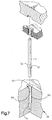
- an electrical module generally indicated at 10 ( Figure 3) is formed from a substrate 12 and a pin blank 14.
- substrate 12 is a printed circuit board and is composed of a dielectric material such as ceramic, fiberglass-reinforced epoxy such as FR4, etc., which contains one or more electrically conductive paths (not shown) therein.
- Substrate 12 defines one or more holes 16 therein which pass all the way through the substrate from a first surface 18 thereof to a second surface 20 thereof.
- hole 16 is a plated-through-hole, meaning that the surfaces of hole 16 carry a coating of an electrically conductive material 22 which extends all the way through the hole from first surface 18 of the substrate to second surface 20 and extends outwardly from the center of the hole by a small distance on these surfaces to form pads 23 as shown in Figure 1.
- the electrically conductive material 22 of the plated-through-hole is electrically connected to an electrically conductive path (not shown) in the substrate.
- pin blank 14 comprises a generally elongated member which defines a first end 24 and a second end 26.
- the body of pin blank 14 near first end 24 defines a substrate-engaging section 28 and, in a location spaced from substrate-engaging section 28, a first compliant section generally indicated at 30.
- first compliant section 30 includes protrusions 32, which are formed by swaging and which extend outwardly from the center line of pin blank 14 by a distance greater than the radius of the pin blank in the remainder of the pin blank body. As discussed more fully below, the shape and size of protrusions 32 are selected so that these protrusions will cooperate with the walls of openings in a second circuit board to which the module 10 is to be attached.
- pin blank 14 is arranged to register with hole 16 in printed circuit board 12.
- printed circuit board 12 and pin blank 14 are also arranged to register with a pin blank receiving hole 34 in a lower hammer 36 as well as a bulge cavity 38 in an upper hammer 40, these hammers being part of a machine (not shown) for attaching pin blanks to boards by compressive deformation.
- Part of pin blank receiving hole 34 in lower hammer 36 defines its own bulge cavity 42 having a shape similar to bulge cavity 38 in upper hammer 40.
- “upper” and “lower” refer to the position as shown in the Figure 1, but physically they can be reversed or even spaced laterally or other direction rather than vertically.
- lower hammer 36 and upper hammer 40 are moved together in the axial direction, i.e., in the direction of the longitudinal axis of pin blank 14.
- This causes the first end 24 of the pin blank to be inserted into hole 16 of board 12 and then for the pin blank to be moved all the way into hole 16 until substrate-engaging section 28 of the pin blank aligns with the body of the board and the end 24 of the pin protrudes out of hole 16 just past pads 23 of electrically conductive material 22.
- movement of the hammers together also causes end 26 and compliant section 30 of pin 14 to be received in pin blank receiving hole 34 of lower hammer 36.
- Figures 1 and 2 illustrate only a single pin blank being affixed to printed circuit board 12, in actual practice there will normally be multiple pin blanks affixed to multiple holes in the substrate.
- a module is provided which, as illustrated in Figure 3, defines a plurality, or array, of pins 14, each having a compliant section projecting from the first surface 18 of the board for subsequent connection of module 10 to another printed circuit board or other device by compliant pin connection, as more fully described below.
- FIGs 4, 5 and 6 illustrate how the inventive module 10 prepared as described above can be connected to another circuit board or other device (known in the art by various terms such as “carrier,” “mother board,” “planar,” etc.) for forming a completed assembly of stacked boards or devices.
- module 10 is arranged so that second end 26 of pin 14 registers with opening 48 in a second electrical substrate 50, which in the embodiment shown is also a printed circuit board.
- Opening 48 in printed circuit board 50 has a size compatible with compliant section 30 of pin 14 so that when this section is inserted into opening 48, protrusions 32 in the compliant section 30 firmly affix pin 14 to circuit board 50 by compliant pin connection.
- the walls of opening 48 in board 50 are plated through holes provided with a coating 52 of an electrically conductive material for providing electrical connection to pin 14 as well as mechanical connection.
- Printed circuit board 50 also includes an electrically conductive path (not shown) connected to the electrically conductive material 52 in hole 48 for electrical connection of pin 14 to other elements on printed circuit board 50.
- module 10 and circuit board 50 With pin 14 arranged in registration with hole 48 of printed circuit 50, module 10 and circuit board 50 are brought together to insert pin 14 into hole 48 of the circuit board.
- This operation is accomplished in the embodiment shown by means of a press 54 and a mounting plate 56.
- Press 54 includes projections 58 for engaging the bulge 46 of pin 14, while mounting plate 56 defines holes 60 for receiving the portion of the body of pin 14 extending out of the bottom of the second printed circuit when module 10 and board 50 are brought together for their final positioning.
- mounting plate 56 and press 54 are brought together until stopped by a suitable stop 62 which is so arranged that converging movement of the press and mounting plate is stopped when protrusions 32 of pin 14 align with the axial center of hole 48.
- suitable spacer elements may also be provided to insure that module 10 and board 50 remain spaced apart by a predetermined distance as press 54 and mounting plate 56 are moved together.
- insertion of compliant section 30 of pin 14 into hole 48 and convergence of press 54 and mounting plate 56 in the manner described above causes compliant section 30 of pin 14 and the walls of hole 48 to be firmly affixed together, thereby creating a secure mechanical and electrical bond in accordance with known compliant pin connection techniques.
- Press 54 and mounting plate 56 are then withdrawn from one another to form a completed assembly 64 as illustrated in Figure 6.
- completed assembly 64 comprises a first circuit board 12 and second circuit board 50 which are securely affixed to one another, both mechanically and electrically by means of pin 14.
- pin 14 In actual practice, many pins will normally be employed rather than the single pin illustrated in the figure so that numerous electrical and mechanical connections can be made, thereby making the connection between boards 12 and 50 even more secure.
- the present invention provides a simple and straightforward method for mechanically and electrically forming together multiple circuit boards in stacked relation without soldering.
- the procedure of the invention requires only simple movement of suitable anvils, hammers and other work pieces in the longitudinal direction, that is the direction aligning with the longitudinal axis of the pin blanks.
- the pin blanks used in the present invention are of simple design, not requiring involved mechanical steps to develop complex shapes or structures as in prior art systems.
- pin blank receiving hole 34 is sized and shaped to receive the lower end of pin 14 therein, even though this portion of pin 14 includes a compliant pin section 30.
- pin blank receiving hole 34 in lower hammer 36 in addition to including bulge cavity 42 as previously described, includes two grooves 66 axially arranged in the walls of pin blank receiving hole 34 to receive protrusions 32 of pin blank 14.
- these grooves 66 extend downwardly by a distance sufficient to accommodate protrusions 32 when pin 14 is inserted in lower hammer 36 by sufficient distance so that the bottom 68 of pin engaging hole 34 engages the end 26 of the pin.
- lower hammer 36 can be used together with upper hammer 40 to cause compressive deformation of pin blank 14 thereby forming bulges 44 and 46 in the manner described above.
- a third electrical substrate or printed circuit board can be stacked with the assembly of two printed circuit boards shown in Figure 6.
- a pin is used which has two compliant sections, one near each of the two ends of the pin blank with the substrate-engaging section being located therebetween.
- the diameter of the substrate-engaging section be larger than the diameter of the pin in the other sections, and preferably at least as large as the largest cross-sectional dimension of the pin at the protrusions 32.
- upper hammer 40 is provided with a pin blank receiving hole having essentially the same structure as pin blank receiving hole 34 in lower hammer 36.
- upper hammer 40 can receive the ends of the pins projecting from the upper surface 20 of board 12 in the same way lower hammer 36 receives the ends of the pins projecting downwardly from lower surface 18 of the board.
- the present invention can be employed to form printed circuit boards, modules, module assemblies and other devices of any size.
- Typical circuit boards used today measure 25 x 25 to 75 x 75 millimeters and contain an array of 5 to 500 pin/holes, for example.
- Conventional pin sizes include pins of 16, 18, 20, etc., mils in diameter with the individual pins being spaced apart by any suitable distance, for example 1.27 to 2.54 millimeters.
- the invention described herein is applicable to printed circuit boards and other electrical devices of any such sizes.
- the present invention is also applicable to the production of printed circuit boards and other electrical devices of even larger construction, with the assemblies once formed being subdivided into smaller subassemblies after formation.
- lower hammer 36 has been described as being a single, unitary member, it should be appreciated that lower hammer 36 can be composed of a number of different pieces or devices so long as the overall function of the hammer remains the same.
- hammer 36 could be divided into two or more pieces, one or more pieces arranged to accept and hold the compliant portion 30 of pin blank 14 and another device employed for the application of axial force to end 26 of the pin blank.
- the electrically conductive material 22 in openings 16 form pads 23 on the first and second surfaces of the substrate, it should be appreciated that such pads are not required.
- using pins and pin blanks of circular cross-section is not required, as any cross-sectional shape can be employed.
- the diameter of the pin blanks used in accordance with the present invention can vary from section to section as desired, it being sufficient in accordance with the present invention merely that hole 34 in hammer 36 (whether formed from single or multiple pieces) receive and accommodate so much of compliant section 30 of the pin as is necessary to accomplish compressive deformation of the pin blank as described above.
- pin blanks with pre-formed compliant sections
- the pin blanks can be affixed to substrate 12 before the pin blank is swaged or otherwise worked to form compliant sections. This, of course, defeats one of the major advantages of the present invention in using preformed pin blanks for the sake of ease of operation and low cost.
Landscapes
- Engineering & Computer Science (AREA)
- Microelectronics & Electronic Packaging (AREA)
- Multi-Conductor Connections (AREA)
- Coupling Device And Connection With Printed Circuit (AREA)
- Manufacturing Of Electrical Connectors (AREA)
Applications Claiming Priority (2)
| Application Number | Priority Date | Filing Date | Title |
|---|---|---|---|
| US08/185,182 US5548486A (en) | 1994-01-21 | 1994-01-21 | Pinned module |
| US185182 | 1994-01-21 |
Publications (2)
| Publication Number | Publication Date |
|---|---|
| EP0664576A2 true EP0664576A2 (fr) | 1995-07-26 |
| EP0664576A3 EP0664576A3 (fr) | 1996-07-31 |
Family
ID=22679944
Family Applications (1)
| Application Number | Title | Priority Date | Filing Date |
|---|---|---|---|
| EP94118583A Withdrawn EP0664576A3 (fr) | 1994-01-21 | 1994-11-25 | Module avec broches de contact. |
Country Status (7)
| Country | Link |
|---|---|
| US (2) | US5548486A (fr) |
| EP (1) | EP0664576A3 (fr) |
| JP (1) | JP2673102B2 (fr) |
| KR (1) | KR100189799B1 (fr) |
| CN (1) | CN1051409C (fr) |
| PH (1) | PH30836A (fr) |
| TW (1) | TW411638B (fr) |
Cited By (6)
| Publication number | Priority date | Publication date | Assignee | Title |
|---|---|---|---|---|
| DE19546888C1 (de) * | 1995-12-15 | 1997-08-21 | Weidmueller Interface | Verfahren zur Bearbeitung einer Anschlußklemme |
| EP0825680A3 (fr) * | 1996-08-23 | 1999-01-27 | CTS Corporation | Connecteur électrique ayant des broches déformables |
| GB2331409A (en) * | 1997-08-06 | 1999-05-19 | Siemens Ag | Housing for electronic control unit |
| WO1999031393A1 (fr) * | 1997-12-15 | 1999-06-24 | Mannesmann Rexroth Ag | Systeme d'assemblage en hauteur |
| CN112787119A (zh) * | 2019-11-05 | 2021-05-11 | 马瑞利汽车照明罗伊特林根(德国)有限公司 | 电路板的导电连接装置 |
| EP3819989A1 (fr) * | 2019-11-05 | 2021-05-12 | Marelli Automotive Lighting Reutlingen (Germany) GmbH | Raccordement électroconducteur de cartes de circuit imprimé |
Families Citing this family (62)
| Publication number | Priority date | Publication date | Assignee | Title |
|---|---|---|---|---|
| US5878483A (en) * | 1995-06-01 | 1999-03-09 | International Business Machines Corporation | Hammer for forming bulges in an array of compliant pin blanks |
| WO1998038700A1 (fr) * | 1997-02-28 | 1998-09-03 | Cornell Research Foundation, Inc. | Ensemble connecteur auto-assemble a faible force d'insertion |
| GB9705277D0 (en) * | 1997-03-14 | 1997-04-30 | Kam Circuits Limited | Improvements relating to printed circuit board pin location |
| US6070531A (en) * | 1997-07-22 | 2000-06-06 | Autoliv Asp, Inc. | Application specific integrated circuit package and initiator employing same |
| US6005198A (en) * | 1997-10-07 | 1999-12-21 | Dimensional Circuits Corporation | Wiring board constructions and methods of making same |
| DE19756345C2 (de) * | 1997-12-18 | 1999-12-30 | Telefunken Microelectron | Anordnung zur Kontaktierung von Leiterplatten |
| US6222739B1 (en) | 1998-01-20 | 2001-04-24 | Viking Components | High-density computer module with stacked parallel-plane packaging |
| US6108902A (en) * | 1998-01-20 | 2000-08-29 | Lucent Technologies, Inc. | Contact pin header connector repair method and repair fixture |
| WO2000014798A1 (fr) * | 1998-09-02 | 2000-03-16 | Ibiden Co., Ltd. | Module de piece electronique monte sur une carte de connexion |
| JP4295384B2 (ja) * | 1999-03-08 | 2009-07-15 | 富士通コンポーネント株式会社 | コネクタ |
| US6448106B1 (en) * | 1999-11-09 | 2002-09-10 | Fujitsu Limited | Modules with pins and methods for making modules with pins |
| US6453549B1 (en) | 1999-12-13 | 2002-09-24 | International Business Machines Corporation | Method of filling plated through holes |
| US6552277B1 (en) * | 2000-09-08 | 2003-04-22 | Emc Corporation | Techniques for forming a connection between a pin and a circuit board |
| US6698091B1 (en) * | 2000-12-29 | 2004-03-02 | Cisco Technology, Inc. | Method and apparatus for coupling circuit boards |
| US6565367B2 (en) | 2001-01-17 | 2003-05-20 | International Business Machines Corporation | Zero insertion force compliant pin contact and assembly |
| US6739881B2 (en) | 2001-05-31 | 2004-05-25 | Trw Inc. | High integration electronic assembly and method |
| KR20020092703A (ko) * | 2001-06-05 | 2002-12-12 | 홍성결 | 씨피유 피씨비 리드핀 및 그 조립방법 |
| US6472970B1 (en) | 2001-06-08 | 2002-10-29 | Trw Inc. | Apparatus for attaching an electric coil to a printed circuit board |
| US6485112B1 (en) | 2001-06-13 | 2002-11-26 | Trw Inc. | Assembly, with lead frame, for antilock brake system and associated method |
| US6518511B1 (en) * | 2001-09-20 | 2003-02-11 | Wen Hsiung Lin | Circuit board having a shortage preventing structure |
| US6549410B1 (en) * | 2001-11-20 | 2003-04-15 | Hewlett-Packard Company | Heatsink mounting system |
| JP4197234B2 (ja) * | 2001-12-28 | 2008-12-17 | 三菱電機株式会社 | 光通信器 |
| US6901646B2 (en) * | 2002-01-16 | 2005-06-07 | Avaya Technology Corp. | Universal snap-fit spacer |
| US6749105B2 (en) | 2002-03-21 | 2004-06-15 | Motorola, Inc. | Method and apparatus for securing a metallic substrate to a metallic housing |
| US6763580B2 (en) | 2002-03-21 | 2004-07-20 | Motorola, Inc. | Method and apparatus for securing an electrically conductive interconnect through a metallic substrate |
| KR100457380B1 (ko) | 2002-05-06 | 2004-11-16 | 삼성전기주식회사 | 광마우스용 칩 온 보드 리드 패키지 및 그에 사용되는렌즈커버 |
| US6716072B1 (en) | 2002-06-27 | 2004-04-06 | Emc Corporation | Systems and methods for disposing a circuit board component on a circuit board using a soldering pin |
| US6716038B2 (en) * | 2002-07-31 | 2004-04-06 | Medallion Technology, Llc | Z-axis connection of multiple substrates by partial insertion of bulges of a pin |
| US6773269B1 (en) * | 2002-09-27 | 2004-08-10 | Emc Corporation | Circuit board assembly which utilizes a pin assembly and techniques for making the same |
| US7135764B2 (en) * | 2003-08-07 | 2006-11-14 | Aries Electronics, Inc. | Shielded semiconductor chip carrier having a high-density external interface |
| DE102004036407A1 (de) * | 2003-08-27 | 2005-06-09 | Japan Electronic Materials Corp., Amagasaki | Prüfkarte und Verbinder für diese |
| JP2005106482A (ja) * | 2003-09-26 | 2005-04-21 | Japan Electronic Materials Corp | 接続ピン |
| JP4131724B2 (ja) * | 2004-10-18 | 2008-08-13 | Tdk株式会社 | 回路基板への端子の取付構造 |
| US7209365B2 (en) * | 2005-04-06 | 2007-04-24 | Inventec Corporation | Card retention device |
| US7242084B2 (en) * | 2005-05-27 | 2007-07-10 | Intel Corporation | Apparatuses and associated methods for improved solder joint reliability |
| US7083431B1 (en) | 2005-09-02 | 2006-08-01 | Lear Corporation | Method and system of electrically connecting multiple printed circuit boards |
| JP2007103079A (ja) * | 2005-09-30 | 2007-04-19 | Funai Electric Co Ltd | Dvd一体型crtテレビジョンおよびコネクタ固定構造 |
| US7300289B2 (en) * | 2005-09-30 | 2007-11-27 | Control Products Inc. | Electrical cordset having connector with integral signal conditioning circuitry |
| US7473101B2 (en) * | 2006-05-05 | 2009-01-06 | International Business Machines Corporation | Connector for mezzanine mounting of a printed wiring board |
| US7503767B2 (en) * | 2006-08-01 | 2009-03-17 | General Dynamics Advanced Information Systems, Inc. | Method and apparatus for compliantly connecting stack of high-density electronic modules in harsh environments |
| US7816781B2 (en) * | 2007-10-02 | 2010-10-19 | Infineon Technologies Ag | Power semiconductor module |
| WO2009046428A2 (fr) * | 2007-10-05 | 2009-04-09 | Battery-Biz® Inc. | Appareil et procédé de raccordement pour composants plats sur cartes de circuit imprimé |
| AT506929B1 (de) * | 2008-04-29 | 2012-10-15 | Siemens Ag | Anordnung zweier schaltungsträger |
| DE102008002558A1 (de) * | 2008-06-20 | 2009-12-24 | Robert Bosch Gmbh | Kontaktstift für eine elektronische Schaltung |
| JP5423621B2 (ja) * | 2010-06-04 | 2014-02-19 | 株式会社デンソー | 回路基板の端子接続構造 |
| KR200456772Y1 (ko) | 2010-10-12 | 2011-11-24 | 주식회사 유라코퍼레이션 | 보드 연결 장치 |
| DE102011054818A1 (de) * | 2011-10-26 | 2013-05-02 | Hella Kgaa Hueck & Co. | Elektronische Schaltung |
| US8900008B2 (en) * | 2012-05-25 | 2014-12-02 | International Business Machines Corporation | Universal press-fit connection for printed circuit boards |
| EP2962365A1 (fr) * | 2013-02-27 | 2016-01-06 | ABB Technology AG | Connecteur de programmation |
| CA2840808C (fr) * | 2013-06-04 | 2016-08-16 | Taketo NISHIKAWA | Structure d'extremite d'un cable mi et sa methode de production |
| US9070987B2 (en) * | 2013-10-30 | 2015-06-30 | Samtec, Inc. | Connector with secure wafer retention |
| JP5681261B1 (ja) * | 2013-10-31 | 2015-03-04 | 株式会社フジクラ | 基板実装端子 |
| CN104797027B (zh) * | 2014-01-20 | 2018-01-02 | 美的集团股份有限公司 | 线圈盘组件 |
| US9554476B2 (en) * | 2014-08-14 | 2017-01-24 | Continental Automotive Systems, Inc. | Compliant staple pin for connecting multiple printed circuit boards |
| CN106298713A (zh) * | 2015-06-09 | 2017-01-04 | 台达电子工业股份有限公司 | 一种垂直连接的功率模块及其堆叠连接的引脚 |
| JP6727937B2 (ja) * | 2016-06-10 | 2020-07-22 | 日本電波工業株式会社 | 電子デバイス |
| CN106535532A (zh) * | 2016-12-27 | 2017-03-22 | 成都芯通科技股份有限公司 | 一种电路系统定位安装装置和定位方法 |
| CN108513440B (zh) * | 2018-04-20 | 2023-11-21 | 深圳市动力飞扬智能装备有限公司 | 一种用于pcb板的上pin包胶设备 |
| TWM584842U (zh) * | 2019-05-10 | 2019-10-11 | 伍鐌科技股份有限公司 | 多扣部之扣件 |
| JP7179434B2 (ja) * | 2020-07-06 | 2022-11-29 | 矢崎総業株式会社 | 車両用計器装置 |
| US11647591B2 (en) | 2021-06-10 | 2023-05-09 | International Business Machines Corporation | Compliant pin surface mount technology pad for rework |
| CN116154502A (zh) * | 2022-12-28 | 2023-05-23 | 太仓神连科技有限公司 | 连接器 |
Family Cites Families (64)
| Publication number | Priority date | Publication date | Assignee | Title |
|---|---|---|---|---|
| US1900099A (en) * | 1929-05-25 | 1933-03-07 | Westinghouse Lamp Co | Method of securing contact pins in radiotube bases |
| US2611010A (en) * | 1949-07-30 | 1952-09-16 | Rca Corp | Printed circuit structure for highfrequency apparatus |
| US2979600A (en) * | 1956-08-31 | 1961-04-11 | Plessey Co Ltd | Electrode systems for electronic valves |
| US3281923A (en) * | 1964-08-27 | 1966-11-01 | Corning Glass Works | Method of attaching leads to thin films |
| US3257708A (en) * | 1965-04-05 | 1966-06-28 | Ibm | Substrate with contact pins and method of making same |
| US3545080A (en) * | 1967-05-16 | 1970-12-08 | Amp Inc | Method of making resilient pins |
| US3541496A (en) * | 1967-12-21 | 1970-11-17 | Thomas & Betts Corp | Terminal |
| US3880486A (en) * | 1973-03-05 | 1975-04-29 | Epis Corp | Apparatus and system for interconnecting circuits and electronic components |
| US3888486A (en) * | 1974-04-10 | 1975-06-10 | Robert E Sutter | Article receiving and collecting receptacle assembly |
| JPS5163460A (en) * | 1974-10-10 | 1976-06-01 | Du Pont | Kairobanpin oyobi hoho |
| DE2541222C2 (de) * | 1974-12-19 | 1982-08-26 | Elfab Corp., Dallas, Tex. | Auf einem Trägerkörper, insbesondere einer Leiterplatte, montierbare Steckvorrichtung |
| JPS52117853A (en) * | 1976-03-29 | 1977-10-03 | Ibm | Detachable solder mask |
| US4034468A (en) * | 1976-09-03 | 1977-07-12 | Ibm Corporation | Method for making conduction-cooled circuit package |
| US4072816A (en) * | 1976-12-13 | 1978-02-07 | International Business Machines Corporation | Integrated circuit package |
| US4082394A (en) * | 1977-01-03 | 1978-04-04 | International Business Machines Corporation | Metallized ceramic and printed circuit module |
| JPS5428586A (en) * | 1977-08-08 | 1979-03-03 | Koden Electronics Co Ltd | Phase tracking malfunction detector for omega receiver |
| US4202007A (en) * | 1978-06-23 | 1980-05-06 | International Business Machines Corporation | Multi-layer dielectric planar structure having an internal conductor pattern characterized with opposite terminations disposed at a common edge surface of the layers |
| US4191938A (en) * | 1978-07-03 | 1980-03-04 | International Business Machines Corporation | Cermet resistor trimming method |
| US4233620A (en) * | 1979-02-27 | 1980-11-11 | International Business Machines Corporation | Sealing of integrated circuit modules |
| US4265775A (en) * | 1979-08-16 | 1981-05-05 | International Business Machines Corporation | Non-bleeding thixotropic thermally conductive material |
| US4274124A (en) * | 1979-12-26 | 1981-06-16 | International Business Machines Corporation | Thick film capacitor having very low internal inductance |
| US4291364A (en) * | 1979-12-26 | 1981-09-22 | International Business Machines Corporation | Air-cooled hybrid electronic package |
| US4415025A (en) * | 1981-08-10 | 1983-11-15 | International Business Machines Corporation | Thermal conduction element for semiconductor devices |
| US4446505A (en) * | 1982-03-22 | 1984-05-01 | Amp Incorporated | Electrical connector for interconnecting printed circuit boards |
| JPS59151443A (ja) * | 1983-02-17 | 1984-08-29 | Fujitsu Ltd | 半導体装置 |
| US4825331A (en) * | 1983-08-29 | 1989-04-25 | Electro-Matic Products Co. | Tape degausser |
| JPS60151030A (ja) * | 1984-01-20 | 1985-08-08 | Japan Styrene Paper Co Ltd | ポリオレフイン系樹脂発泡成型体の製造方法 |
| US4550493A (en) * | 1984-02-08 | 1985-11-05 | International Business Machines Corporation | Apparatus for connecting contact pins to a substrate |
| GB8412674D0 (en) * | 1984-05-18 | 1984-06-27 | British Telecomm | Integrated circuit chip carrier |
| JPS6110263A (ja) * | 1984-06-26 | 1986-01-17 | Nec Kansai Ltd | ハイブリツドic |
| US4601424A (en) * | 1985-05-17 | 1986-07-22 | International Business Machines Corporation | Stripped gold plating process |
| JPS62136865A (ja) * | 1985-12-11 | 1987-06-19 | Hitachi Ltd | モジユ−ル実装構造 |
| JPS62271376A (ja) * | 1986-01-31 | 1987-11-25 | デイジタル イクイプメント コ−ポレ−シヨン | 回路板連結用プレス嵌めピン |
| US4780371A (en) * | 1986-02-24 | 1988-10-25 | International Business Machines Corporation | Electrically conductive composition and use thereof |
| US4676426A (en) * | 1986-03-10 | 1987-06-30 | Ibm Corp. | Solder leveling technique |
| JPS62216259A (ja) * | 1986-03-17 | 1987-09-22 | Fujitsu Ltd | 混成集積回路の製造方法および構造 |
| US4690833A (en) * | 1986-03-28 | 1987-09-01 | International Business Machines Corporation | Providing circuit lines on a substrate |
| JPS62287658A (ja) * | 1986-06-06 | 1987-12-14 | Hitachi Ltd | セラミックス多層回路板 |
| US4741100A (en) * | 1986-09-24 | 1988-05-03 | International Business Machines Corporation | Pin retention method and apparatus |
| US4803595A (en) * | 1986-11-17 | 1989-02-07 | International Business Machines Corporation | Interposer chip technique for making engineering changes between interconnected semiconductor chips |
| US4764848A (en) * | 1986-11-24 | 1988-08-16 | International Business Machines Corporation | Surface mounted array strain relief device |
| US5159535A (en) * | 1987-03-11 | 1992-10-27 | International Business Machines Corporation | Method and apparatus for mounting a flexible film semiconductor chip carrier on a circuitized substrate |
| JPS63241892A (ja) * | 1987-03-30 | 1988-10-07 | 藤好 克聡 | 端子等の製造方法 |
| US4813130A (en) * | 1987-04-23 | 1989-03-21 | International Business Machines | Automatic extrusion pinning method and apparatus |
| US4791075A (en) * | 1987-10-05 | 1988-12-13 | Motorola, Inc. | Process for making a hermetic low cost pin grid array package |
| JP2548602B2 (ja) * | 1988-04-12 | 1996-10-30 | 株式会社日立製作所 | 半導体実装モジュール |
| US4889496A (en) * | 1988-04-12 | 1989-12-26 | Intercon Systems, Inc. | Compressible core electrical connector |
| US4988646A (en) * | 1988-05-12 | 1991-01-29 | International Business Machines | Method for producing a ceramic |
| US4883744A (en) * | 1988-05-17 | 1989-11-28 | International Business Machines Corporation | Forming a polymide pattern on a substrate |
| US4916259A (en) * | 1988-08-01 | 1990-04-10 | International Business Machines Corporation | Composite dielectric structure for optimizing electrical performance in high performance chip support packages |
| US4878861A (en) * | 1988-11-01 | 1989-11-07 | Elfab Corporation | Compliant electrical connector pin |
| JPH02125696A (ja) * | 1988-11-04 | 1990-05-14 | Nec Corp | 多層印刷配線板 |
| JPH02155176A (ja) * | 1988-12-06 | 1990-06-14 | Ngk Spark Plug Co Ltd | 金属端子の固定方法 |
| US4969259A (en) * | 1988-12-14 | 1990-11-13 | International Business Machines Corporation | Pin with tubular elliptical compliant portion and method for affixing to mating receptacle |
| JP3090453B2 (ja) * | 1989-07-10 | 2000-09-18 | 株式会社日立製作所 | 厚膜薄膜積層基板およびそれを用いた電子回路装置 |
| US5082460A (en) * | 1989-10-02 | 1992-01-21 | Zierick Manufacturing Corporation | Electrical terminal with frangible mounting leg and method of forming the same |
| JPH0574532A (ja) * | 1990-01-18 | 1993-03-26 | Kel Corp | 電気コネクタ |
| US5002507A (en) * | 1990-01-31 | 1991-03-26 | E. I. Du Pont De Nemours And Company | Circuit board contact element and compliant section thereof |
| JPH03263771A (ja) * | 1990-03-13 | 1991-11-25 | Fujitsu Ltd | プレスフィットピン |
| US5065227A (en) * | 1990-06-04 | 1991-11-12 | International Business Machines Corporation | Integrated circuit packaging using flexible substrate |
| US5050296A (en) * | 1990-06-07 | 1991-09-24 | International Business Machines Corporation | Affixing pluggable pins to a ceramic substrate |
| US5048178A (en) * | 1990-10-23 | 1991-09-17 | International Business Machines Corp. | Alignment--registration tool for fabricating multi-layer electronic packages |
| US5257165A (en) * | 1992-02-13 | 1993-10-26 | Jaton Technology Co., Ltd. | Pin grid array adaptor mounting hardware |
| DE9203996U1 (de) * | 1992-03-25 | 1992-05-07 | Schroff Gmbh, 75334 Straubenhardt | Elektronisches Modul |
-
1994
- 1994-01-21 US US08/185,182 patent/US5548486A/en not_active Expired - Fee Related
- 1994-09-21 JP JP6226511A patent/JP2673102B2/ja not_active Expired - Lifetime
- 1994-11-25 EP EP94118583A patent/EP0664576A3/fr not_active Withdrawn
- 1994-12-29 KR KR1019940038855A patent/KR100189799B1/ko not_active Expired - Fee Related
- 1994-12-29 PH PH49724A patent/PH30836A/en unknown
- 1994-12-31 CN CN94113423A patent/CN1051409C/zh not_active Expired - Fee Related
-
1995
- 1995-01-13 TW TW084100279A patent/TW411638B/zh not_active IP Right Cessation
- 1995-06-01 US US08/457,413 patent/US5715595A/en not_active Expired - Fee Related
Cited By (9)
| Publication number | Priority date | Publication date | Assignee | Title |
|---|---|---|---|---|
| DE19546888C1 (de) * | 1995-12-15 | 1997-08-21 | Weidmueller Interface | Verfahren zur Bearbeitung einer Anschlußklemme |
| EP0825680A3 (fr) * | 1996-08-23 | 1999-01-27 | CTS Corporation | Connecteur électrique ayant des broches déformables |
| GB2331409A (en) * | 1997-08-06 | 1999-05-19 | Siemens Ag | Housing for electronic control unit |
| US6180880B1 (en) | 1997-08-06 | 2001-01-30 | Siemens Aktiengesellschaft | Electronic control unit with a contact pin, and method of producing the control unit |
| GB2331409B (en) * | 1997-08-06 | 2001-08-08 | Siemens Ag | Electronic control unit |
| WO1999031393A1 (fr) * | 1997-12-15 | 1999-06-24 | Mannesmann Rexroth Ag | Systeme d'assemblage en hauteur |
| CN112787119A (zh) * | 2019-11-05 | 2021-05-11 | 马瑞利汽车照明罗伊特林根(德国)有限公司 | 电路板的导电连接装置 |
| EP3819989A1 (fr) * | 2019-11-05 | 2021-05-12 | Marelli Automotive Lighting Reutlingen (Germany) GmbH | Raccordement électroconducteur de cartes de circuit imprimé |
| EP3819988A1 (fr) * | 2019-11-05 | 2021-05-12 | Marelli Automotive Lighting Reutlingen (Germany) GmbH | Raccordement électroconducteur de cartes de circuit imprimé |
Also Published As
| Publication number | Publication date |
|---|---|
| JP2673102B2 (ja) | 1997-11-05 |
| US5715595A (en) | 1998-02-10 |
| CN1111833A (zh) | 1995-11-15 |
| TW411638B (en) | 2000-11-11 |
| KR950024623A (ko) | 1995-08-21 |
| JPH07220779A (ja) | 1995-08-18 |
| CN1051409C (zh) | 2000-04-12 |
| KR100189799B1 (ko) | 1999-06-01 |
| EP0664576A3 (fr) | 1996-07-31 |
| PH30836A (en) | 1997-11-03 |
| US5548486A (en) | 1996-08-20 |
Similar Documents
| Publication | Publication Date | Title |
|---|---|---|
| US5548486A (en) | Pinned module | |
| US5601453A (en) | Electrical connector hold-down | |
| EP0373342B1 (fr) | Assemblage de plaque de circuit et borne de contact utilisable dans ce circuit | |
| US7097506B2 (en) | Contact module in which mounting of contacts is simplified | |
| US4923414A (en) | Compliant section for circuit board contact elements | |
| EP0825680B1 (fr) | Connecteur électrique ayant des broches déformables | |
| EP0088582B1 (fr) | Bornes électriques fixées par pression | |
| JPH09511865A (ja) | 低背電気コネクタ | |
| US5878483A (en) | Hammer for forming bulges in an array of compliant pin blanks | |
| US6483041B1 (en) | Micro soldered connection | |
| DE19649549C1 (de) | Anordnung, insbesondere zur Verwendung in einem elektronischen Steuergerät, und Verfahren zur Herstellung derselben | |
| US9093775B2 (en) | Connection pin for mounting in a component carrier, a method for producing an electronic assembly comprising a motherboard with stackable modules comprising a component carrier, and such an electronic assembly | |
| US20040253863A1 (en) | Floating connector and method for manufacturing therefor | |
| EP2679082B1 (fr) | Broche de connexion et son procédé de montage dans un porte-composant pour ensemble électronique, et porte-composant de ce type comprenant des broches de connexion | |
| EP0418045A1 (fr) | Connecteur à broches coaxiales avec une rangée de structures cylindriques conductrices creuses | |
| JP2000501225A (ja) | 滑らかなコンタクト端子を形成する方法 | |
| US5017159A (en) | Solid single leg terminal | |
| US7185430B2 (en) | Method of manufacturing contact sheets | |
| US12030103B2 (en) | Assembly with a stack of sheet metal joined from at least three superimposed layers of sheet metal | |
| JPH0245305B2 (fr) | ||
| EP2679081B1 (fr) | Procédé de montage de broches de connexion dans un porte-composant, outil de matrice pour montage de broches de connexion, porte-composant constituant un module pour un ensemble électronique, et ensemble électronique | |
| JPH033344B2 (fr) | ||
| JP2003142191A (ja) | リセプタクルコンタクトおよびその製造方法 | |
| JPS63181283A (ja) | コネクタの製造方法 | |
| TW202304288A (zh) | 用於將部件固定在一起的壓配合緊固件 |
Legal Events
| Date | Code | Title | Description |
|---|---|---|---|
| PUAI | Public reference made under article 153(3) epc to a published international application that has entered the european phase |
Free format text: ORIGINAL CODE: 0009012 |
|
| AK | Designated contracting states |
Kind code of ref document: A2 Designated state(s): DE FR GB |
|
| 17P | Request for examination filed |
Effective date: 19951115 |
|
| PUAL | Search report despatched |
Free format text: ORIGINAL CODE: 0009013 |
|
| AK | Designated contracting states |
Kind code of ref document: A3 Designated state(s): DE FR GB |
|
| STAA | Information on the status of an ep patent application or granted ep patent |
Free format text: STATUS: THE APPLICATION HAS BEEN WITHDRAWN |
|
| 18W | Application withdrawn |
Withdrawal date: 19961125 |