EP0664628A2 - Übertragungssteuerungsvorrichtung - Google Patents
Übertragungssteuerungsvorrichtung Download PDFInfo
- Publication number
- EP0664628A2 EP0664628A2 EP94120140A EP94120140A EP0664628A2 EP 0664628 A2 EP0664628 A2 EP 0664628A2 EP 94120140 A EP94120140 A EP 94120140A EP 94120140 A EP94120140 A EP 94120140A EP 0664628 A2 EP0664628 A2 EP 0664628A2
- Authority
- EP
- European Patent Office
- Prior art keywords
- signal
- line
- outputting
- error
- data
- Prior art date
- Legal status (The legal status is an assumption and is not a legal conclusion. Google has not performed a legal analysis and makes no representation as to the accuracy of the status listed.)
- Withdrawn
Links
Images


Classifications
-
- H—ELECTRICITY
- H04—ELECTRIC COMMUNICATION TECHNIQUE
- H04L—TRANSMISSION OF DIGITAL INFORMATION, e.g. TELEGRAPHIC COMMUNICATION
- H04L12/00—Data switching networks
- H04L12/28—Data switching networks characterised by path configuration, e.g. LAN [Local Area Networks] or WAN [Wide Area Networks]
- H04L12/40—Bus networks
- H04L12/40006—Architecture of a communication node
- H04L12/40013—Details regarding a bus controller
-
- H—ELECTRICITY
- H04—ELECTRIC COMMUNICATION TECHNIQUE
- H04L—TRANSMISSION OF DIGITAL INFORMATION, e.g. TELEGRAPHIC COMMUNICATION
- H04L69/00—Network arrangements, protocols or services independent of the application payload and not provided for in the other groups of this subclass
- H04L69/40—Network arrangements, protocols or services independent of the application payload and not provided for in the other groups of this subclass for recovering from a failure of a protocol instance or entity, e.g. service redundancy protocols, protocol state redundancy or protocol service redirection
-
- H—ELECTRICITY
- H04—ELECTRIC COMMUNICATION TECHNIQUE
- H04L—TRANSMISSION OF DIGITAL INFORMATION, e.g. TELEGRAPHIC COMMUNICATION
- H04L12/00—Data switching networks
- H04L12/28—Data switching networks characterised by path configuration, e.g. LAN [Local Area Networks] or WAN [Wide Area Networks]
- H04L12/40—Bus networks
- H04L12/407—Bus networks with decentralised control
- H04L12/413—Bus networks with decentralised control with random access, e.g. carrier-sense multiple-access with collision detection [CSMA-CD]
- H04L12/4135—Bus networks with decentralised control with random access, e.g. carrier-sense multiple-access with collision detection [CSMA-CD] using bit-wise arbitration
-
- H—ELECTRICITY
- H04—ELECTRIC COMMUNICATION TECHNIQUE
- H04L—TRANSMISSION OF DIGITAL INFORMATION, e.g. TELEGRAPHIC COMMUNICATION
- H04L43/00—Arrangements for monitoring or testing data switching networks
-
- H—ELECTRICITY
- H04—ELECTRIC COMMUNICATION TECHNIQUE
- H04L—TRANSMISSION OF DIGITAL INFORMATION, e.g. TELEGRAPHIC COMMUNICATION
- H04L43/00—Arrangements for monitoring or testing data switching networks
- H04L43/08—Monitoring or testing based on specific metrics, e.g. QoS, energy consumption or environmental parameters
- H04L43/0823—Errors, e.g. transmission errors
- H04L43/0847—Transmission error
Definitions
- FIG. 3 is a schematic diagram showing a pulse width modulated bit pattern defined in a PWM (pulse width modulation) bit format of "Class B data communication network interface JI850" above stated.
- reference numerals 11 and 12 indicate the BUS+line and BUS-line, respectively shown in FIG. 1, and a plurality of nodes of the same configuration indicated by reference symbol N are connected to these lines 11 and 12.
- Reference numeral 16 indicates a transmit buffer memory in which data to be transmitted.
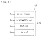
- the transmission buffer memory 16 stores each data of the priority code 2, destination address 3, self address 4 and data area 5 comprising the transmit frame 10 shown in FIG. 2.
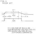
- An output voltage V25 of the second differential comparator 25 whereto the signals from the BUS+line 11 and a voltage V23 (VDD/2) of the reference power supply 23 are inputted goes high ("H" level) when a voltage V11 of the BUS+line 11 is higher than the reference voltage V23 (VDD/2) and goes low ("L" level) when the former is lower than the latter as shown in FIG. 9.
- the communication controlling apparatus related to the present invention has error detecting means; wherein in the case where a circuit error is detected in one transmission line, the output gate is not immediately disabled but error detection data is transmitted from its own node and then whether a transmission line error is detected or not for the error detection data transmitted from it is determined.
- the P-channel MOS transistor 20 its source is connected to the power supply voltage VDD, its gate is connected to the output terminal of the NAND gate 18, and its drain is connected to the BUS+line 11 as well as grounded via a pull-down resistance 34.
- the N-channel MOS transistor 21 its source is connected to ground voltage GND, its gate is connected to the output terminal of the AND gate 19, and its drain is connected to the BUS-line 12 as well as the power supply voltage VDD via a pull-up resistance 35.
- the transmit data selector 171 in the transmit frame composing circuit 17 selects the data stored in the transmit buffer memory 16 by the transmit data select signal 31a given from the sequence control circuit 31.
- the transmit frame composing circuit 17 which is activated start to send data in the case where the line is not busy.
- Data transmitted in this case is in order of the SOF 1, priority code 2, and a broadcast code as the destination address 3 as shown in FIG. 17.
- the broadcast code is the one which can transmit the same one frame data to all the nodes.
- the node sends the self address 4 and "data 1" as the data area 5 indicating the line wherein an error is detected by the node; in this way, all the other nodes are notified that an error is detected by the node.
- FIG. 7 of the schematic diagram showing a state wherein an error has occurred FIG. 18 of the waveform diagram showing the operations performed in an error node
- FIG. 19 of the waveforms showing the operations of the nodes other than error node FIG. 20 of the waveform diagram showing the state at receiving operation after finishing the processing.
- the sequence control circuit 31 gives the selector control signal 311 (27a, 27b, 27c), wherein the signal 27a becomes"H" level and the signal 27b becomes “L” level, to the selector 27 shown in FIG. 14.
- the selector 27 selects the output signal 251, as the receive data, of the second differential comparator 25 instead of the output signal 241 of the first differential comparator 24.
- the sequence control circuit 31 makes the transmit frame composing circuit 17 compose the transmit frame 10 for the data 32a shown in FIG. 12 stored in the error detecting frame buffer 32 and sends out it at a timing T12.
- the sequence control circuit 31 makes the signal 27a from “L” level to “H” level and the signal 27b from “H” level to “L” level with the selector control signal 311 (27a, 27b, 27c) to select the output signal 251 of the second differential comparator 25 instead of the output signal 241 of the first differential comparator 24 as the receive data.
- the sequence control circuit 31 makes the transmit frame composing circuit 17 compose the transmit frame 10 for the data 32a shown in FIG. 12 stored in the error detecting frame buffer 32 and sends it at the timing T12 as the frame 303.
- each node N2, N3 ⁇ detects an error in the BUS-line 12 at the timing T22 and makes the error signal 30b in "H" level.
- the selector control signal 27a is kept in "H” level after reception of the SOF 1, and then receiving processing of the output signal 251 of the second differential comparator 25 operated by the BUS+line 11 is performed.
- each the node N2, N3 ⁇ receives the third byte of the transmit frame 201. It is the address of the first node N1.
- Each node N2, N3 ⁇ compares the received third byte with the error node address (the address of the first node N1 in this case) received in the frame 302 stated above and stored in the error node address memory 33 and the error contents (error in the BUS-line 12 in this case); and when they coincide, each node N2, N3 ⁇ does not perform operation for the time when an error has occurred as described in FIG. 18 and FIG. 19 but makes the error signal 30b in "L" level for indicating error detection in the BUS-line 12.
- Data contents of frame 304 sent out from the nodes N2, N3 ⁇ other than the first node N1 is sent out according to the frame format shown in FIG. 2.
- the broadcast code as the destination address 3 located in the second byte
- the self address (the address of the first node N1) as the self address 4 located in the third byte
- the sequence control circuit 31 gives transmit data select signals 31f and 31g in addition to the transmit data select signal 31a to the transmit data selector 171.
- the transmit data select signal 31f becomes in "H" level when an error is detected.
- the transmit data selector 171 selects the data 32d shown in FIG. 26 as a transmit data and outputs it to the PtoS shift register 172.
- the transmit data select signal 31g goes high when no error is detected. This makes the transmit data selector 171 select the data 32e shown in FIG. 27 above as a transmit data and outputs it to the PtoS shift register 172.
- the sequence control circuit 31 makes the signal 27a in “H” level from “L” level, and makes the signal 27b in “L” level from “H” level among the selector control signal 311 (27a, 27b, 27c), to the selector 27 to select the output signal 251 of from the second differential comparator 25 instead of the output signal 241 of the first differential comparator 24 as the receive data.
- the SOF 1 is transmitted.
- the sequence control circuit 31 changes the transmit data select signal 31g in "H” level and gives it to the transmit data selector 171 at the timing T43.
- the transmit data selector 171 upon changing the transmit data select signal 31g in "H” level, selects the data 32e shown in FIG. 27 stored in the error detecting frame buffer 32.
- the data 32e is transmitted following the SOF 1 which is sent out at the timing T42 as the frame 306 corresponding to the frame format shown in FIG. 2.
- the communication controlling apparatus related to the present invention has controlling means; wherein in the case where its own node has detected a circuit error, the error informing data is sent to all the other nodes. Therefore one of the lines can be selected for data transfer between the nodes which have detected no errors. This improves the reliability of communication.
- the communication controlling apparatus related to the present invention has controlling means; wherein in the case where its own node has detected no error, the error informing data to that effect is sent to all the other nodes.
- the nodes which have detected transmission line errors can be known.
Landscapes
- Engineering & Computer Science (AREA)
- Computer Networks & Wireless Communication (AREA)
- Signal Processing (AREA)
- Computer Security & Cryptography (AREA)
- Detection And Prevention Of Errors In Transmission (AREA)
- Maintenance And Management Of Digital Transmission (AREA)
Applications Claiming Priority (2)
| Application Number | Priority Date | Filing Date | Title |
|---|---|---|---|
| JP322588/93 | 1993-12-21 | ||
| JP5322588A JPH07177202A (ja) | 1993-12-21 | 1993-12-21 | 通信制御装置 |
Publications (1)
| Publication Number | Publication Date |
|---|---|
| EP0664628A2 true EP0664628A2 (de) | 1995-07-26 |
Family
ID=18145379
Family Applications (1)
| Application Number | Title | Priority Date | Filing Date |
|---|---|---|---|
| EP94120140A Withdrawn EP0664628A2 (de) | 1993-12-21 | 1994-12-19 | Übertragungssteuerungsvorrichtung |
Country Status (3)
| Country | Link |
|---|---|
| US (1) | US5528754A (de) |
| EP (1) | EP0664628A2 (de) |
| JP (1) | JPH07177202A (de) |
Cited By (2)
| Publication number | Priority date | Publication date | Assignee | Title |
|---|---|---|---|---|
| EP0827872A3 (de) * | 1996-09-09 | 2000-04-12 | Ford Motor Company | Verfahren und System zur Erkennung von Fehlerbedingungen in Multiplexnetzwerken |
| WO2000041458A3 (de) * | 1999-01-14 | 2000-11-16 | Siemens Ag | Verfahren und einrichtung zur sendesignalüberwachung |
Families Citing this family (5)
| Publication number | Priority date | Publication date | Assignee | Title |
|---|---|---|---|---|
| US6037779A (en) * | 1997-09-17 | 2000-03-14 | Chrysler Corporation | Bus isolation/diagnostic tool |
| CA2280571A1 (en) * | 1998-11-30 | 2000-05-30 | Daimlerchrysler Corporation | J1850 application specific integrated circuit (asic) and messaging technique |
| DE10340034A1 (de) * | 2003-08-28 | 2005-03-31 | Pierburg Gmbh | Potentiometervorrichtung zur Erfassung von Ventilpositionen |
| JP4419067B2 (ja) * | 2004-07-26 | 2010-02-24 | 株式会社日立製作所 | ディジタルインターフェースを有する半導体装置、メモリ素子及びメモリモジュール |
| TWI876760B (zh) * | 2022-12-23 | 2025-03-11 | 立錡科技股份有限公司 | 上拉電壓偵測電路與上拉電壓偵測方法 |
Family Cites Families (5)
| Publication number | Priority date | Publication date | Assignee | Title |
|---|---|---|---|---|
| BE794181A (nl) * | 1971-12-01 | 1973-07-18 | Int Standard Electric Corp | Inrichting voor het bepalen van de soort en de plaats van fouten bij de overdracht van gegevenstekens |
| US4527271A (en) * | 1982-08-17 | 1985-07-02 | The Foxboro Company | Process control system with improved fault isolation |
| JPH0752886B2 (ja) * | 1987-12-19 | 1995-06-05 | 富士通株式会社 | ループ型ネットワークの構成方法 |
| FR2654564B1 (fr) * | 1989-11-10 | 1992-01-17 | Renault | Interface de ligne pour un reseau de transmission d'informations. |
| JP2513919B2 (ja) * | 1990-09-05 | 1996-07-10 | 株式会社日立製作所 | 構成制御装置の再構成機能停止防止方式 |
-
1993
- 1993-12-21 JP JP5322588A patent/JPH07177202A/ja active Pending
-
1994
- 1994-12-19 EP EP94120140A patent/EP0664628A2/de not_active Withdrawn
- 1994-12-20 US US08/359,769 patent/US5528754A/en not_active Expired - Fee Related
Cited By (2)
| Publication number | Priority date | Publication date | Assignee | Title |
|---|---|---|---|---|
| EP0827872A3 (de) * | 1996-09-09 | 2000-04-12 | Ford Motor Company | Verfahren und System zur Erkennung von Fehlerbedingungen in Multiplexnetzwerken |
| WO2000041458A3 (de) * | 1999-01-14 | 2000-11-16 | Siemens Ag | Verfahren und einrichtung zur sendesignalüberwachung |
Also Published As
| Publication number | Publication date |
|---|---|
| JPH07177202A (ja) | 1995-07-14 |
| US5528754A (en) | 1996-06-18 |
Similar Documents
| Publication | Publication Date | Title |
|---|---|---|
| US6839789B2 (en) | Bus repeater for coupling a first and second bus | |
| CN103282895B (zh) | 以高数据率串行传输数据的装置和方法 | |
| CA1283228C (en) | Multiplex transmission system | |
| CN110892681B (zh) | 发送/接收装置、总线系统及识别短路的方法 | |
| US20020108011A1 (en) | Dual interface serial bus | |
| JP7042899B2 (ja) | バスシステム用の振動低減ユニットおよび異なるビット状態間の移行時の振動傾向を低減する方法 | |
| JP2851124B2 (ja) | 多重伝送方式 | |
| US11343118B2 (en) | User station for a serial bus system and method for transmitting a message in a serial bus system | |
| US11567892B2 (en) | Bus transceiver | |
| US5528754A (en) | Communication controlling apparatus | |
| US10848419B2 (en) | Data transmission method, communication network and master participant | |
| EP0589499A1 (de) | Mehrstationskommunikationsbussystem, sowie eine Master-Station und eine Slave-Station für den Einsatz in einem solchen System | |
| JP2753915B2 (ja) | 通信制御装置 | |
| CN112859663A (zh) | 具有可切换的转换速率的现场总线系统 | |
| EP0893019B1 (de) | Verfahren und schnittsstellenschaltung für multiplex-kommunikation | |
| EP0300263B1 (de) | Schwacher/starker Bustreiber | |
| EP1009136B1 (de) | Gesteuerte Stromquelle für Leitungstreiber beziehungsweise Leitungsempfänger | |
| EP1989630B1 (de) | Schnittstelle zwischen bussen verschiedener physikalischer schichten | |
| JPH05300155A (ja) | 多重伝送方式 | |
| KR100226781B1 (ko) | 노드(node)인식(recognition)방법 | |
| CN111164937A (zh) | 用于总线系统的发送/接收装置和用于减小在不同的位状态之间过渡时的振荡趋势的方法 | |
| US5384778A (en) | Communication control apparatus | |
| EP4164185A2 (de) | Controller area network sender/empfänger | |
| KR930702867A (ko) | 데이터의 송수신 방법 및 그 장치 | |
| JP2026015974A (ja) | 半導体装置、および通信システム |
Legal Events
| Date | Code | Title | Description |
|---|---|---|---|
| PUAI | Public reference made under article 153(3) epc to a published international application that has entered the european phase |
Free format text: ORIGINAL CODE: 0009012 |
|
| AK | Designated contracting states |
Kind code of ref document: A2 Designated state(s): DE FR GB |
|
| STAA | Information on the status of an ep patent application or granted ep patent |
Free format text: STATUS: THE APPLICATION IS DEEMED TO BE WITHDRAWN |
|
| 18D | Application deemed to be withdrawn |
Effective date: 20000701 |