EP0665584A1 - Verfahren zum Umhüllen einer elektronischen Bauteils mit härtbarem Kunststoff, elektronische Bauteile mit Kunststoffumhüllung und Gussform zum Ausführen dieses Verfahrens - Google Patents
Verfahren zum Umhüllen einer elektronischen Bauteils mit härtbarem Kunststoff, elektronische Bauteile mit Kunststoffumhüllung und Gussform zum Ausführen dieses Verfahrens Download PDFInfo
- Publication number
- EP0665584A1 EP0665584A1 EP95200178A EP95200178A EP0665584A1 EP 0665584 A1 EP0665584 A1 EP 0665584A1 EP 95200178 A EP95200178 A EP 95200178A EP 95200178 A EP95200178 A EP 95200178A EP 0665584 A1 EP0665584 A1 EP 0665584A1
- Authority
- EP
- European Patent Office
- Prior art keywords
- component
- mould
- plastic
- film
- encasing
- Prior art date
- Legal status (The legal status is an assumption and is not a legal conclusion. Google has not performed a legal analysis and makes no representation as to the accuracy of the status listed.)
- Granted
Links
Images


Classifications
-
- B—PERFORMING OPERATIONS; TRANSPORTING
- B29—WORKING OF PLASTICS; WORKING OF SUBSTANCES IN A PLASTIC STATE IN GENERAL
- B29C—SHAPING OR JOINING OF PLASTICS; SHAPING OF MATERIAL IN A PLASTIC STATE, NOT OTHERWISE PROVIDED FOR; AFTER-TREATMENT OF THE SHAPED PRODUCTS, e.g. REPAIRING
- B29C33/00—Moulds or cores; Details thereof or accessories therefor
- B29C33/10—Moulds or cores; Details thereof or accessories therefor with incorporated venting means
-
- B—PERFORMING OPERATIONS; TRANSPORTING
- B29—WORKING OF PLASTICS; WORKING OF SUBSTANCES IN A PLASTIC STATE IN GENERAL
- B29C—SHAPING OR JOINING OF PLASTICS; SHAPING OF MATERIAL IN A PLASTIC STATE, NOT OTHERWISE PROVIDED FOR; AFTER-TREATMENT OF THE SHAPED PRODUCTS, e.g. REPAIRING
- B29C33/00—Moulds or cores; Details thereof or accessories therefor
- B29C33/56—Coatings, e.g. enameled or galvanised; Releasing, lubricating or separating agents
- B29C33/68—Release sheets
-
- B—PERFORMING OPERATIONS; TRANSPORTING
- B29—WORKING OF PLASTICS; WORKING OF SUBSTANCES IN A PLASTIC STATE IN GENERAL
- B29C—SHAPING OR JOINING OF PLASTICS; SHAPING OF MATERIAL IN A PLASTIC STATE, NOT OTHERWISE PROVIDED FOR; AFTER-TREATMENT OF THE SHAPED PRODUCTS, e.g. REPAIRING
- B29C45/00—Injection moulding, i.e. forcing the required volume of moulding material through a nozzle into a closed mould; Apparatus therefor
- B29C45/14—Injection moulding, i.e. forcing the required volume of moulding material through a nozzle into a closed mould; Apparatus therefor incorporating preformed parts or layers, e.g. injection moulding around inserts or for coating articles
- B29C45/14639—Injection moulding, i.e. forcing the required volume of moulding material through a nozzle into a closed mould; Apparatus therefor incorporating preformed parts or layers, e.g. injection moulding around inserts or for coating articles for obtaining an insulating effect, e.g. for electrical components
- B29C45/14655—Injection moulding, i.e. forcing the required volume of moulding material through a nozzle into a closed mould; Apparatus therefor incorporating preformed parts or layers, e.g. injection moulding around inserts or for coating articles for obtaining an insulating effect, e.g. for electrical components connected to or mounted on a carrier, e.g. lead frame
-
- B—PERFORMING OPERATIONS; TRANSPORTING
- B29—WORKING OF PLASTICS; WORKING OF SUBSTANCES IN A PLASTIC STATE IN GENERAL
- B29C—SHAPING OR JOINING OF PLASTICS; SHAPING OF MATERIAL IN A PLASTIC STATE, NOT OTHERWISE PROVIDED FOR; AFTER-TREATMENT OF THE SHAPED PRODUCTS, e.g. REPAIRING
- B29C45/00—Injection moulding, i.e. forcing the required volume of moulding material through a nozzle into a closed mould; Apparatus therefor
- B29C45/17—Component parts, details or accessories; Auxiliary operations
- B29C45/26—Moulds
- B29C45/34—Moulds having venting means
- B29C45/345—Moulds having venting means using a porous mould wall or a part thereof, e.g. made of sintered metal
-
- B—PERFORMING OPERATIONS; TRANSPORTING
- B29—WORKING OF PLASTICS; WORKING OF SUBSTANCES IN A PLASTIC STATE IN GENERAL
- B29C—SHAPING OR JOINING OF PLASTICS; SHAPING OF MATERIAL IN A PLASTIC STATE, NOT OTHERWISE PROVIDED FOR; AFTER-TREATMENT OF THE SHAPED PRODUCTS, e.g. REPAIRING
- B29C45/00—Injection moulding, i.e. forcing the required volume of moulding material through a nozzle into a closed mould; Apparatus therefor
- B29C45/17—Component parts, details or accessories; Auxiliary operations
- B29C45/46—Means for plasticising or homogenising the moulding material or forcing it into the mould
- B29C45/462—Injection of preformed charges of material
- B29C45/463—Injection of preformed charges of material using packaged or wrapped charges
-
- H—ELECTRICITY
- H10—SEMICONDUCTOR DEVICES; ELECTRIC SOLID-STATE DEVICES NOT OTHERWISE PROVIDED FOR
- H10W—GENERIC PACKAGES, INTERCONNECTIONS, CONNECTORS OR OTHER CONSTRUCTIONAL DETAILS OF DEVICES COVERED BY CLASS H10
- H10W74/00—Encapsulations, e.g. protective coatings
- H10W74/01—Manufacture or treatment
- H10W74/016—Manufacture or treatment using moulds
- H10W74/017—Auxiliary layers for moulds, e.g. release layers or layers preventing residue
-
- B—PERFORMING OPERATIONS; TRANSPORTING
- B29—WORKING OF PLASTICS; WORKING OF SUBSTANCES IN A PLASTIC STATE IN GENERAL
- B29C—SHAPING OR JOINING OF PLASTICS; SHAPING OF MATERIAL IN A PLASTIC STATE, NOT OTHERWISE PROVIDED FOR; AFTER-TREATMENT OF THE SHAPED PRODUCTS, e.g. REPAIRING
- B29C45/00—Injection moulding, i.e. forcing the required volume of moulding material through a nozzle into a closed mould; Apparatus therefor
- B29C45/14—Injection moulding, i.e. forcing the required volume of moulding material through a nozzle into a closed mould; Apparatus therefor incorporating preformed parts or layers, e.g. injection moulding around inserts or for coating articles
- B29C45/14639—Injection moulding, i.e. forcing the required volume of moulding material through a nozzle into a closed mould; Apparatus therefor incorporating preformed parts or layers, e.g. injection moulding around inserts or for coating articles for obtaining an insulating effect, e.g. for electrical components
- B29C45/14655—Injection moulding, i.e. forcing the required volume of moulding material through a nozzle into a closed mould; Apparatus therefor incorporating preformed parts or layers, e.g. injection moulding around inserts or for coating articles for obtaining an insulating effect, e.g. for electrical components connected to or mounted on a carrier, e.g. lead frame
- B29C2045/14663—Injection moulding, i.e. forcing the required volume of moulding material through a nozzle into a closed mould; Apparatus therefor incorporating preformed parts or layers, e.g. injection moulding around inserts or for coating articles for obtaining an insulating effect, e.g. for electrical components connected to or mounted on a carrier, e.g. lead frame the mould cavity walls being lined with a film, e.g. release film
-
- H—ELECTRICITY
- H10—SEMICONDUCTOR DEVICES; ELECTRIC SOLID-STATE DEVICES NOT OTHERWISE PROVIDED FOR
- H10W—GENERIC PACKAGES, INTERCONNECTIONS, CONNECTORS OR OTHER CONSTRUCTIONAL DETAILS OF DEVICES COVERED BY CLASS H10
- H10W72/00—Interconnections or connectors in packages
- H10W72/01—Manufacture or treatment
- H10W72/0198—Manufacture or treatment batch processes
Definitions
- the invention relates to a method for encasing an electronic component, in particular an integrated circuit, with a hardening plastic, in which the component is positioned in the cavity of a splittable mould, with a film, which is detachable from the walls of the cavity, placed between the component and the mould and the plastic being injected into the space between the component and the film.
- a method for encasing an electronic component in particular an integrated circuit
- a hardening plastic in which the component is positioned in the cavity of a splittable mould, with a film, which is detachable from the walls of the cavity, placed between the component and the mould and the plastic being injected into the space between the component and the film.
- This known method has many advantages, such as the absence of release agent in the plastic used for the encasing, the fact that the mould is not subject to wear by the abrasive fillers in the plastic, and a good and complete detachment of the encased components from the mould.
- the invention aims to improve this known method and is based on the insight that particularly interesting and advantageous applications arise when one uses a film which at the side facing the component bears a material which adheres better to the still warm plastic encasing the component than to the film, sothat this material remains adhering to the plastic encasement during and after the removal of same from the mould after it has cooled.
- the material can be applied to the encasement of an electronic component either as a full coating, or as a partial coating, with the possibility to provide the outer surface of such a component with all kinds of patterns.
- the material can be a metal, resulting into a metal coating.
- the material can also be a ceramic material, or glass.
- This glass can be applied to the film in a pattern of light-conducting tracks, which can be combined with, or made to interact with, light-sensitive or radiation-sensitive electronic components. These light-conducting tracks can also be combined with, or made to interact with, light-transmitting or radiation-transmitting electronic components.
- the claimed exclusive rights also include an electronic component with plastic encasement, provided with a coating applied by means of the above described method.
- This coating can either be a metal coating which can have the form of discrete tracks, to which electronic components are connected, or a coating of ceramic material, such as glass. This can be in the form of tracks interacting with electronic radiation-sensitive and/or radiation-transmitting components.
- the injection pressure is maintained during the carrying out of the second step.
- the claimed exclusive rights also include a mould for carrying out the above described method provided with means for controlling the closure of the moulding cavity walls in such a way that in a first step said walls are moved virtually completely into their end position with compacting of the plastic, and in a second, succeeding step are moved into their end position.
- This mould is preferably provided with a shut-off element in the injection channel.
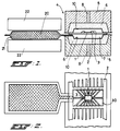
- Fig. 1 shows a section of a known mould by means of which the method according to the invention can be carried out.
- Reference numeral 1 indicates a semi-conductor component, in particular an integrated circuit, mounted on a lead frame strip 2.
- the electrical connections of the semi-conductor component 1 are connected to the lead frame strip 2 by means of wires 3.
- the lead frame strip is clamped between two parts of the mould 4.
- the mould 4 consists of two shoes 5, containing porous moulding parts 6 which define cavities 7 in the mould.
- the shoes 5 have channels 8, by means of which air can be extracted from the moulding parts 6 or admitted to the moulding parts.
- the inside walls of the mould parts are covered with a stretchable film 10 which does not adhere to the plastic, and does not adhere to the mould either.
- the film is fitted closely against the moulding part through extraction of the air from the space between the moulding part 6 and the film 10.
- the cavity 7 provided with film is subsequently filled by injecting a liquid, hardening plastic 20, for example by forcing said plastic out of a flexible encasement 21 between two pressure plates 22.
- the cavity has a vent, for example a gap in the partial face of the mould 4.
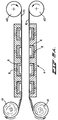
- Fig. 2 shows a top view of the device according to Fig. 1, with top part 5, 6 of the mould removed and the pressure plate 22 removed. Parts with identical reference numbers to those in Fig. 1 are of the same type and have the same function.
- the horizontal boundary of a cavity 7 in the mould is indicated by the dashed line 30.
- Various semi-conductor components 1 are generally mounted on the lead frame strip 2 through repetition of the illustrated structure upwards and/or downwards in the figure.
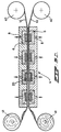
- Fig. 3 illustrates in succession in Figs. 3A, 3B, 3C, 3D and 3E the processing steps to be carried out in an embodiment of the method according to the invention. Parts with identical reference numberals to those in Fig. 1 or Fig. 2 are of the same type and have the same function.
- Fig. 3A shows an open mould 4, consisting of two parts, between which two flat bands of film 10 are stretched, one for each mould part.
- Each band of film comes off a stock roll 40, from where the film, after being used once, is rolled onto a second roll 41, as shown in Figs. 3B, 3C, 3D and 3E.
- the rolls 40 and 41 can be, for example, braked and driven in a manner not shown in any further detail, in such a way that the film is held taut in the mould.
- Fig. 3B shows the next step.
- the moulding parts, with the unused bands of film between them, are clamped together, following which the air is extracted through the channels 8 between the porous moulding parts 6 and the film 10. This is symbolized by the arrows facing away from the mould at the channels 8.
- the film which is stretchable, is deformed so that it fits closely against the cavities 7, and thus forms a layer on the inside wall of the mould parts.
- Fig. 3C shows the subsequent opening of the mould, while the film remains sucked against the moulding parts 6.
- a lead frame strip 2 with in this example four semi-conductor components 1 mounted thereon, is positioned between the mould parts and thereby clamped fast after the mould parts have been brought together.
- Fig. 3D illustrates the next step according to the new method, in which a hardening plastic 20 is forced into the cavities provided with semi-conductor components, lead frame strip and film.
- Fig. 3E gives an example of the detachment from the closed mould of the semi-conductor components on the lead frame strip encased with set plastic.
- air can be supplied through the channels 8 of the top mould part to the porous moulding parts 6 of the top mould part (symbolized by the arrows facing the mould at the channels 8), following which the mould is opened.
- the top film now comes away from the top moulding parts, from the top mould part and from the encased semi-conductor components, since the film does not adhere to the materials in question.
- the components are detached in a corresponding way from the bottom mould part, following which the components are removed from the mould.
- the parts of the films 10 used in the mould are then wound onto the rolls 41, following which the situation illustrated in Fig. 3A arises again.
- the method according to the invention offers particularly interesting applications by using a film bearing on the side facing the component a material which adheres better to the still warm plastic encasing the component than to the film, and thus remains adhering to the plastic encasement following removal thereof from the mould after cooling.
- the material consists of a metal coating
- a Faraday cage is formed around the component, by means of which the component is protected against incoming electromagnetic radiation, and the discharge of electromagnetic radiation is also suppressed. Moreover, a certain protection against the penetration of moisture is obtained, and radiation in the visible light spectrum and in the ultraviolet spectrum will also be blocked.
- a special advantage is that the metal layer offers the possibility of soldering the component in a simple manner to a metal element, for example a cooling element.
- Partially pressing away the carrier film mass at the transition from the clamping face around the moulding cavity and the moulding cavity itself ensures that the coating is stretched through stretching of the elastic carrier film, in such a way that the non-elastic metal layer can no longer follow this stretch and is interrupted, so that the contacts coming out of the electronic component are prevented from short-circuiting with each other.
- a second possibility is the use of a ceramic material. This gives an absolute shielding of the encased component and a considerably improved protection against penetration of moisture, because there are many fewer moisture-absorbent molecules on the external surface of the product thus obtained than is the case with a plastic surface not shielded with ceramic material.
- This complete sealing against moisture penetration means that there is no risk now of "blowing up” through steam formation, which could occur where there is great local heating during, for example, soldering or if a large quantity of electrical energy is dissipated in the encased component, with the accompanying heat development.
- far-reaching protection against radiation from the visible and ultraviolet spectrum can be obtained.
- porous moulding parts 6 shown in Figs. 1 and 3 are not absolutely essential for achieving the object according to the invention.
- a single air venting or air supply opening, or a limited number of such openings in the cavity 7, connected to an air channel 8, can replace the porous mould part, this depending on the stretching properties of the film.
- a film which has the abovementioned properties is, for example, a polymer film.
- the mould cavity walls are not yet fully in their end position, and the plastic is injected between the component and the film at such pressure that the film comes to rest sealingly against the moulding cavity walls. Thereafter, the mould cavity walls are taken into the end position, which causes the pressure in the mould cavity to increase sharply, resulting in good sealing of the moulding mass at the critical points where air inclusions are often found if the encasing is carried out in one step.
- moulds which are not fully closed in the first step, and in the case of which the sealing effect of the film is therefore relied upon for the sealing, but it is preferable to use a mould in which the moulding cavity walls themselves are movable more or less independently of the mould.
- the mould is then fully closed, but the moulding cavity walls have not yet reached their definitive end position; the latter is not achieved until the second step, during which the moulding mass is compacted.
- shut-off element is provided in the injection channel.
Landscapes
- Engineering & Computer Science (AREA)
- Mechanical Engineering (AREA)
- Manufacturing & Machinery (AREA)
- Encapsulation Of And Coatings For Semiconductor Or Solid State Devices (AREA)
- Injection Moulding Of Plastics Or The Like (AREA)
- Apparatuses And Processes For Manufacturing Resistors (AREA)
- Moulds For Moulding Plastics Or The Like (AREA)
- Details Of Resistors (AREA)
- Casting Or Compression Moulding Of Plastics Or The Like (AREA)
- Packaging Frangible Articles (AREA)
- Processing And Handling Of Plastics And Other Materials For Molding In General (AREA)
- Non-Metallic Protective Coatings For Printed Circuits (AREA)
Applications Claiming Priority (2)
| Application Number | Priority Date | Filing Date | Title |
|---|---|---|---|
| NL9400119 | 1994-01-27 | ||
| NL9400119A NL9400119A (nl) | 1994-01-27 | 1994-01-27 | Werkwijze voor het met een hardende kunststof omhullen van een electronische component, electronische componenten met kunststofomhulling verkregen door middel van deze werkwijze en matrijs voor het uitvoeren der werkwijze. |
Publications (2)
| Publication Number | Publication Date |
|---|---|
| EP0665584A1 true EP0665584A1 (de) | 1995-08-02 |
| EP0665584B1 EP0665584B1 (de) | 1999-04-07 |
Family
ID=19863746
Family Applications (1)
| Application Number | Title | Priority Date | Filing Date |
|---|---|---|---|
| EP95200178A Expired - Lifetime EP0665584B1 (de) | 1994-01-27 | 1995-01-25 | Verfahren zum Umhüllen eines elektronischen Bauteils mit härtbarem Kunststoff |
Country Status (11)
| Country | Link |
|---|---|
| EP (1) | EP0665584B1 (de) |
| JP (2) | JP3169315B2 (de) |
| KR (2) | KR100327500B1 (de) |
| AT (1) | ATE178737T1 (de) |
| DE (1) | DE69508815T2 (de) |
| ES (1) | ES2130513T3 (de) |
| MY (2) | MY131118A (de) |
| NL (1) | NL9400119A (de) |
| RU (1) | RU2139597C1 (de) |
| SG (1) | SG55005A1 (de) |
| TW (1) | TW257737B (de) |
Cited By (27)
| Publication number | Priority date | Publication date | Assignee | Title |
|---|---|---|---|---|
| EP0728567A1 (de) * | 1995-02-22 | 1996-08-28 | Apic Yamada Corporation | Verfahren und Maschine zum Giessen von Kunststoff |
| EP0730937A1 (de) * | 1994-11-21 | 1996-09-11 | Apic Yamada Corporation | Harzformmaschine mit Trennfolie |
| NL1000777C2 (nl) * | 1995-07-11 | 1997-01-14 | 3P Licensing Bv | Werkwijze voor het inkapselen van een elektronische component, elektronische component geschikt te worden toegepast bij het uitvoeren van deze werkwijze en ingekapselde component verkregen onder toepassing der werkwijze. |
| EP0713248A3 (de) * | 1994-11-17 | 1997-04-23 | Hitachi Ltd | Giessverfahren und Vorrichtung dafür |
| EP0747942A3 (de) * | 1995-05-02 | 1998-07-29 | Texas Instruments Incorporated | Verbesserungen in oder in Beziehung auf integrierte Schaltungen |
| US5800841A (en) * | 1994-11-24 | 1998-09-01 | Apic Yamada Corporation | Resin molding machine |
| US5891483A (en) * | 1995-08-23 | 1999-04-06 | Apic Yamada Corp. | Automatic molding machine using release film |
| EP0795901A3 (de) * | 1996-03-14 | 1999-10-27 | Towa Corporation | Verfahren zum Einkapseln eines elektronischen Bauelements mit vergossenem Harz |
| EP0971401A2 (de) | 1998-07-10 | 2000-01-12 | Apic Yamada Corporation | Verfahren zur Herstellung einer Halbleitervorrichtung und Harzformmaschine zu diesem Zweck |
| EP0933808A3 (de) * | 1998-01-23 | 2000-03-22 | Apic Yamada Corporation | Verfahren und Vorrichtung zur Harzversiegelung einer Halbleitervorrichtung |
| US6048483A (en) * | 1996-07-23 | 2000-04-11 | Apic Yamada Corporation | Resin sealing method for chip-size packages |
| US6080354A (en) * | 1997-05-01 | 2000-06-27 | Apic Yamada Corporation | Resin molding method in which a movable cavity piece allows a direct resin feed |
| NL1011392C2 (nl) * | 1999-02-25 | 2000-08-28 | 3P Licensing Bv | Inrichting voor het omhullen van elektronische componenten en daarvoor bestemde matrijs. |
| US6187243B1 (en) | 1997-07-11 | 2001-02-13 | Apic Yamada Corporation | Method of resin molding |
| US6630374B2 (en) * | 2000-01-19 | 2003-10-07 | Towa Corporation | Resin sealing method and resin sealing apparatus |
| EP1366897A1 (de) * | 2002-05-30 | 2003-12-03 | SOL S.p.A. | Verfahren zum Formen eines verformbaren Materials in einer Hülle |
| WO2007073579A1 (en) * | 2005-12-29 | 2007-07-05 | Bluescope Steel Limited | Method of making a composite product |
| WO2010069961A1 (en) * | 2008-12-18 | 2010-06-24 | Novartis Ag | Mold release sheet |
| US20110271902A1 (en) * | 2008-11-17 | 2011-11-10 | Advanpack Solutions Pte Ltd. | System For Encapsulation Of Semiconductor Dies |
| WO2013066162A1 (en) * | 2011-10-18 | 2013-05-10 | Fico B.V. | Method and device for encapsulating electronic components using a reduction material which undergoes a phase change |
| DE102012109144A1 (de) * | 2012-09-27 | 2014-04-17 | Osram Opto Semiconductors Gmbh | Bauteilanordnung und Verfahren zum Herstellen von optischen Bauteilen |
| NL2011512C2 (en) * | 2013-09-26 | 2015-03-30 | Besi Netherlands B V | Method for moulding and surface processing electronic components and electronic component produced with this method. |
| WO2018185373A1 (en) * | 2017-04-07 | 2018-10-11 | Tactotek Oy | Method for manufacturing an electronic assembly and an electronic assembly |
| CN110076953A (zh) * | 2014-09-29 | 2019-08-02 | 日亚化学工业株式会社 | 封装的制造方法、发光装置的制造方法及封装、发光装置 |
| US11305471B2 (en) * | 2017-11-20 | 2022-04-19 | Coexpair S.A. | Resin supply systems |
| US11318642B2 (en) | 2019-12-20 | 2022-05-03 | Eaton Intelligent Power Limited | Permeable wall encapsulation mold |
| CN117719137A (zh) * | 2024-02-06 | 2024-03-19 | 河南君源塑业有限公司 | 聚氯乙烯板材加工用挤压成型装置及其成型工艺 |
Families Citing this family (11)
| Publication number | Priority date | Publication date | Assignee | Title |
|---|---|---|---|---|
| US6881611B1 (en) | 1996-07-12 | 2005-04-19 | Fujitsu Limited | Method and mold for manufacturing semiconductor device, semiconductor device and method for mounting the device |
| RU2202842C2 (ru) * | 2000-06-02 | 2003-04-20 | Северо-Осетинский государственный университет им. К.Л.Хетагурова | Композиция для защиты бескорпусных высоковольтных полупроводниковых приборов |
| DE10108253C1 (de) * | 2001-02-21 | 2002-07-11 | Bayern Chemie Gmbh Flugchemie | Verfahren zur Herstellung von aus fliessfähigem Material bestehenden Gegenständen |
| US6567630B1 (en) | 2002-02-01 | 2003-05-20 | Toshiba Tec Kabushiki Kaisha | Image forming device |
| JP4540415B2 (ja) * | 2004-07-16 | 2010-09-08 | パナソニック株式会社 | 音響整合部材の製造方法 |
| JP5119221B2 (ja) * | 2009-08-31 | 2013-01-16 | ルネサスエレクトロニクス株式会社 | 半導体集積回路装置の製造方法 |
| KR101101669B1 (ko) * | 2009-12-01 | 2011-12-30 | 삼성전기주식회사 | 전자부품 제조장치 및 전자부품 제조방법 |
| US9734304B2 (en) | 2011-12-02 | 2017-08-15 | Lumiradx Uk Ltd | Versatile sensors with data fusion functionality |
| US9700222B2 (en) | 2011-12-02 | 2017-07-11 | Lumiradx Uk Ltd | Health-monitor patch |
| CN103465419A (zh) * | 2013-09-16 | 2013-12-25 | 铜陵荣鑫机械有限公司 | 大功率led球形封装成型机 |
| CN114434751B (zh) * | 2022-03-18 | 2024-07-16 | 珠海格力精密模具有限公司 | 仿生透气装置及注塑模具 |
Citations (7)
| Publication number | Priority date | Publication date | Assignee | Title |
|---|---|---|---|---|
| FR2103917A5 (de) * | 1970-08-03 | 1972-04-14 | Motorola Inc | |
| JPS63250846A (ja) * | 1987-04-08 | 1988-10-18 | Hitachi Ltd | 面付実装用lsiプラスチツクパツケ−ジとその製造方法 |
| JPS6444056A (en) * | 1987-08-11 | 1989-02-16 | Nec Corp | Hybrid integrated circuit |
| JPS6444026A (en) * | 1987-08-11 | 1989-02-16 | Michio Osada | Resin-seal formation of component to be sealed and heat resistant sheet member used therefor |
| EP0350179A1 (de) * | 1988-06-21 | 1990-01-10 | Gec Avery Limited | Herstellung von tragbaren elektronischen Karten |
| WO1991010546A1 (en) * | 1990-01-11 | 1991-07-25 | Swerad Heat Radiating Concrete Ab | A mould for moulding of a thermosetting substance |
| EP0442152A1 (de) * | 1990-02-13 | 1991-08-21 | Kabushiki Kaisha Toshiba | Kunstharz-Giessvorrichtung |
Family Cites Families (2)
| Publication number | Priority date | Publication date | Assignee | Title |
|---|---|---|---|---|
| US4641418A (en) * | 1982-08-30 | 1987-02-10 | International Rectifier Corporation | Molding process for semiconductor devices and lead frame structure therefor |
| US5169586A (en) * | 1990-05-21 | 1992-12-08 | Nec Corporation | Method of manufacturing resin-sealed type semiconductor device |
-
1994
- 1994-01-27 NL NL9400119A patent/NL9400119A/nl not_active Application Discontinuation
-
1995
- 1995-01-11 TW TW084100215A patent/TW257737B/zh active
- 1995-01-19 MY MYPI20010065A patent/MY131118A/en unknown
- 1995-01-19 MY MYPI95000117A patent/MY118471A/en unknown
- 1995-01-21 KR KR1019950001034A patent/KR100327500B1/ko not_active Expired - Fee Related
- 1995-01-25 DE DE69508815T patent/DE69508815T2/de not_active Expired - Fee Related
- 1995-01-25 AT AT95200178T patent/ATE178737T1/de not_active IP Right Cessation
- 1995-01-25 ES ES95200178T patent/ES2130513T3/es not_active Expired - Lifetime
- 1995-01-25 SG SG1996001596A patent/SG55005A1/en unknown
- 1995-01-25 EP EP95200178A patent/EP0665584B1/de not_active Expired - Lifetime
- 1995-01-26 RU RU95101033A patent/RU2139597C1/ru active
- 1995-01-27 JP JP01186195A patent/JP3169315B2/ja not_active Expired - Fee Related
-
2001
- 2001-02-01 JP JP2001025092A patent/JP2001260149A/ja active Pending
- 2001-02-26 KR KR1020010009618A patent/KR100336873B1/ko not_active Expired - Fee Related
Patent Citations (7)
| Publication number | Priority date | Publication date | Assignee | Title |
|---|---|---|---|---|
| FR2103917A5 (de) * | 1970-08-03 | 1972-04-14 | Motorola Inc | |
| JPS63250846A (ja) * | 1987-04-08 | 1988-10-18 | Hitachi Ltd | 面付実装用lsiプラスチツクパツケ−ジとその製造方法 |
| JPS6444056A (en) * | 1987-08-11 | 1989-02-16 | Nec Corp | Hybrid integrated circuit |
| JPS6444026A (en) * | 1987-08-11 | 1989-02-16 | Michio Osada | Resin-seal formation of component to be sealed and heat resistant sheet member used therefor |
| EP0350179A1 (de) * | 1988-06-21 | 1990-01-10 | Gec Avery Limited | Herstellung von tragbaren elektronischen Karten |
| WO1991010546A1 (en) * | 1990-01-11 | 1991-07-25 | Swerad Heat Radiating Concrete Ab | A mould for moulding of a thermosetting substance |
| EP0442152A1 (de) * | 1990-02-13 | 1991-08-21 | Kabushiki Kaisha Toshiba | Kunstharz-Giessvorrichtung |
Non-Patent Citations (3)
| Title |
|---|
| PATENT ABSTRACTS OF JAPAN vol. 013, no. 062 (E - 715) 13 February 1989 (1989-02-13) * |
| PATENT ABSTRACTS OF JAPAN vol. 013, no. 240 (E - 767) 6 June 1989 (1989-06-06) * |
| PATENT ABSTRACTS OF JAPAN vol. 013, no. 243 (E - 768) 7 June 1989 (1989-06-07) * |
Cited By (51)
| Publication number | Priority date | Publication date | Assignee | Title |
|---|---|---|---|---|
| EP0713248A3 (de) * | 1994-11-17 | 1997-04-23 | Hitachi Ltd | Giessverfahren und Vorrichtung dafür |
| EP0730937A1 (de) * | 1994-11-21 | 1996-09-11 | Apic Yamada Corporation | Harzformmaschine mit Trennfolie |
| US5891384A (en) * | 1994-11-21 | 1999-04-06 | Apic Yamada Corporation | Method of operating a molding machine with release film |
| US5800841A (en) * | 1994-11-24 | 1998-09-01 | Apic Yamada Corporation | Resin molding machine |
| US6444157B1 (en) | 1994-11-24 | 2002-09-03 | Apic Yamada Corporation | Method of resin molding |
| EP0728567A1 (de) * | 1995-02-22 | 1996-08-28 | Apic Yamada Corporation | Verfahren und Maschine zum Giessen von Kunststoff |
| US5949132A (en) * | 1995-05-02 | 1999-09-07 | Texas Instruments Incorporated | Dambarless leadframe for molded component encapsulation |
| EP0747942A3 (de) * | 1995-05-02 | 1998-07-29 | Texas Instruments Incorporated | Verbesserungen in oder in Beziehung auf integrierte Schaltungen |
| NL1000777C2 (nl) * | 1995-07-11 | 1997-01-14 | 3P Licensing Bv | Werkwijze voor het inkapselen van een elektronische component, elektronische component geschikt te worden toegepast bij het uitvoeren van deze werkwijze en ingekapselde component verkregen onder toepassing der werkwijze. |
| EP0753888A3 (de) * | 1995-07-11 | 1997-07-09 | 3P Licensing Bv | Verfahren zum Umhüllen eines elektronischen Bauelementes und nach diesem Verfahren hergestellter Gegenstand |
| SG96162A1 (en) * | 1995-08-23 | 2003-05-23 | Apic Yamada Corp | Automatic molding machine using release film |
| US5891483A (en) * | 1995-08-23 | 1999-04-06 | Apic Yamada Corp. | Automatic molding machine using release film |
| EP0759349B1 (de) * | 1995-08-23 | 2002-06-05 | Apic Yamada Corporation | Automatische Formmaschine mit Trennfolie |
| EP0795901A3 (de) * | 1996-03-14 | 1999-10-27 | Towa Corporation | Verfahren zum Einkapseln eines elektronischen Bauelements mit vergossenem Harz |
| US6048483A (en) * | 1996-07-23 | 2000-04-11 | Apic Yamada Corporation | Resin sealing method for chip-size packages |
| US6224360B1 (en) | 1996-07-23 | 2001-05-01 | Apic Yamada Corporation | Resin sealing device for chip-size packages |
| US6080354A (en) * | 1997-05-01 | 2000-06-27 | Apic Yamada Corporation | Resin molding method in which a movable cavity piece allows a direct resin feed |
| US6350113B1 (en) | 1997-07-11 | 2002-02-26 | Apic Yamada Corporation | Resin molding machine |
| US6187243B1 (en) | 1997-07-11 | 2001-02-13 | Apic Yamada Corporation | Method of resin molding |
| US6459159B1 (en) | 1998-01-23 | 2002-10-01 | Apic Yamada Corporation | Apparatus for sealing a semiconductor device utilizing a release film |
| EP0933808A3 (de) * | 1998-01-23 | 2000-03-22 | Apic Yamada Corporation | Verfahren und Vorrichtung zur Harzversiegelung einer Halbleitervorrichtung |
| SG96180A1 (en) * | 1998-01-23 | 2003-05-23 | Apic Yamada Corp | Resin sealing method and apparatus for a semiconductor device |
| EP0971401A3 (de) * | 1998-07-10 | 2001-06-13 | Apic Yamada Corporation | Verfahren zur Herstellung einer Halbleitervorrichtung und Harzformmaschine zu diesem Zweck |
| EP0971401A2 (de) | 1998-07-10 | 2000-01-12 | Apic Yamada Corporation | Verfahren zur Herstellung einer Halbleitervorrichtung und Harzformmaschine zu diesem Zweck |
| US6344162B1 (en) | 1998-07-10 | 2002-02-05 | Apic Yamada Corporation | Method of manufacturing semiconductor devices and resin molding machine |
| NL1011392C2 (nl) * | 1999-02-25 | 2000-08-28 | 3P Licensing Bv | Inrichting voor het omhullen van elektronische componenten en daarvoor bestemde matrijs. |
| SG104934A1 (en) * | 2000-01-19 | 2004-07-30 | Towa Corp | Resin sealing method and resin sealing apparatus |
| US6630374B2 (en) * | 2000-01-19 | 2003-10-07 | Towa Corporation | Resin sealing method and resin sealing apparatus |
| BE1014855A5 (nl) * | 2002-05-30 | 2004-05-04 | Sol Spa | Het vormgeven in een omhulling. |
| EP1366897A1 (de) * | 2002-05-30 | 2003-12-03 | SOL S.p.A. | Verfahren zum Formen eines verformbaren Materials in einer Hülle |
| WO2007073579A1 (en) * | 2005-12-29 | 2007-07-05 | Bluescope Steel Limited | Method of making a composite product |
| US9082775B2 (en) * | 2008-11-17 | 2015-07-14 | Advanpack Solutions Pte Ltd | System for encapsulation of semiconductor dies |
| US20110271902A1 (en) * | 2008-11-17 | 2011-11-10 | Advanpack Solutions Pte Ltd. | System For Encapsulation Of Semiconductor Dies |
| WO2010069961A1 (en) * | 2008-12-18 | 2010-06-24 | Novartis Ag | Mold release sheet |
| US8944795B2 (en) | 2008-12-18 | 2015-02-03 | Novartis Ag | Mold release sheet |
| WO2013066162A1 (en) * | 2011-10-18 | 2013-05-10 | Fico B.V. | Method and device for encapsulating electronic components using a reduction material which undergoes a phase change |
| GB2516148A (en) * | 2011-10-18 | 2015-01-14 | Besi Netherlands Bv | Method and device for encapsulating electronic components using a reduction material which undergoes a phase change |
| GB2516148B (en) * | 2011-10-18 | 2016-10-26 | Besi Netherlands Bv | Method and device for encapsulating electronic components using a reduction material which undergoes a phase change |
| DE102012109144A1 (de) * | 2012-09-27 | 2014-04-17 | Osram Opto Semiconductors Gmbh | Bauteilanordnung und Verfahren zum Herstellen von optischen Bauteilen |
| NL2011512C2 (en) * | 2013-09-26 | 2015-03-30 | Besi Netherlands B V | Method for moulding and surface processing electronic components and electronic component produced with this method. |
| CN110076953A (zh) * | 2014-09-29 | 2019-08-02 | 日亚化学工业株式会社 | 封装的制造方法、发光装置的制造方法及封装、发光装置 |
| CN110076953B (zh) * | 2014-09-29 | 2021-06-04 | 日亚化学工业株式会社 | 封装的制造方法、发光装置的制造方法及封装、发光装置 |
| WO2018185373A1 (en) * | 2017-04-07 | 2018-10-11 | Tactotek Oy | Method for manufacturing an electronic assembly and an electronic assembly |
| US11285645B2 (en) | 2017-04-07 | 2022-03-29 | Tactotek Oy | Method for manufacturing an electronic assembly and an electronic assembly |
| US11292166B2 (en) | 2017-04-07 | 2022-04-05 | Tactotek Oy | Method for manufacturing an electronic assembly and an electronic assembly |
| US11305471B2 (en) * | 2017-11-20 | 2022-04-19 | Coexpair S.A. | Resin supply systems |
| EP4234217A3 (de) * | 2017-11-20 | 2023-10-25 | Coexpair S.A. | Harzzuführsystem für das kunstharztransferformen, und darauf bezogenes verfahren |
| US11318642B2 (en) | 2019-12-20 | 2022-05-03 | Eaton Intelligent Power Limited | Permeable wall encapsulation mold |
| EP4076886B1 (de) * | 2019-12-20 | 2025-02-12 | Eaton Intelligent Power Limited | Verkapselungsform für durchlässige wand |
| CN117719137A (zh) * | 2024-02-06 | 2024-03-19 | 河南君源塑业有限公司 | 聚氯乙烯板材加工用挤压成型装置及其成型工艺 |
| CN117719137B (zh) * | 2024-02-06 | 2024-05-03 | 河南君源塑业有限公司 | 聚氯乙烯板材加工用挤压成型装置及其成型工艺 |
Also Published As
| Publication number | Publication date |
|---|---|
| DE69508815T2 (de) | 1999-11-11 |
| KR950034712A (ko) | 1995-12-28 |
| SG55005A1 (en) | 1998-12-21 |
| MY118471A (en) | 2004-11-30 |
| JP2001260149A (ja) | 2001-09-25 |
| RU2139597C1 (ru) | 1999-10-10 |
| KR100336873B1 (ko) | 2002-05-15 |
| ATE178737T1 (de) | 1999-04-15 |
| RU95101033A (ru) | 1996-10-27 |
| DE69508815D1 (de) | 1999-05-12 |
| NL9400119A (nl) | 1995-09-01 |
| TW257737B (de) | 1995-09-21 |
| JPH07283260A (ja) | 1995-10-27 |
| HK1006124A1 (en) | 1999-02-12 |
| KR100327500B1 (ko) | 2002-08-08 |
| EP0665584B1 (de) | 1999-04-07 |
| JP3169315B2 (ja) | 2001-05-21 |
| ES2130513T3 (es) | 1999-07-01 |
| MY131118A (en) | 2007-07-31 |
Similar Documents
| Publication | Publication Date | Title |
|---|---|---|
| EP0665584B1 (de) | Verfahren zum Umhüllen eines elektronischen Bauteils mit härtbarem Kunststoff | |
| US3960635A (en) | Method for the fabrication of printed circuits | |
| EP0890425B1 (de) | Verfahren zum Formen von Kunststoff und Kunststoffformmaschine | |
| US7101737B2 (en) | Method of encapsulating interconnecting units in packaged microelectronic devices | |
| US5422313A (en) | Integrated circuit device and manufacturing method using photoresist lead covering | |
| MY114173A (en) | Method for producing semiconductor device | |
| EP0747942A3 (de) | Verbesserungen in oder in Beziehung auf integrierte Schaltungen | |
| US6399004B1 (en) | Method for encapsulating a chip on a carrier | |
| HK1006124B (en) | Method for encasing an electronic component with a hardening plastic | |
| US5157820A (en) | Capacitor manufacturing process | |
| JP2700449B2 (ja) | 電子パワーデバイスのヒートシンクを電気的に絶縁するための方法および装置 | |
| KR100677007B1 (ko) | 반도체 장치를 캡슐화하기 위한 사출 성형 시스템 및 그방법 | |
| US5083193A (en) | Semiconductor package, method of manufacturing the same, apparatus for carrying out the method, and assembly facility | |
| JP3658258B2 (ja) | 半導体装置の製造方法 | |
| JP2000133666A (ja) | 半導体パッケ―ジ用金型 | |
| US7241414B2 (en) | Method and apparatus for molding a semiconductor device | |
| JP2934174B2 (ja) | 電子部品の製造方法 | |
| JP2004055738A (ja) | 離型フィルムの供給方法及び供給装置 | |
| EP4191642A3 (de) | Verfahren zum einkapseln von doppelseitigen gekühlten verpackungen | |
| JPS6298733A (ja) | 半導体装置の樹脂封止用金型 | |
| JPS63162206A (ja) | 樹脂成形装置 | |
| JPH01297830A (ja) | 半導体素子の薄型封止方法 | |
| JPH07297338A (ja) | リードフレーム | |
| EP0753888A2 (de) | Verfahren zum Umhüllen eines elektronischen Bauelementes und nach diesem Verfahren hergestellter Gegenstand | |
| JPH05315508A (ja) | 絶縁タイバー付きのリードフレーム及びその製造方法 |
Legal Events
| Date | Code | Title | Description |
|---|---|---|---|
| PUAI | Public reference made under article 153(3) epc to a published international application that has entered the european phase |
Free format text: ORIGINAL CODE: 0009012 |
|
| 17P | Request for examination filed |
Effective date: 19950426 |
|
| AK | Designated contracting states |
Kind code of ref document: A1 Designated state(s): AT BE CH DE ES FR GB IE IT LI LU NL PT SE |
|
| 17Q | First examination report despatched |
Effective date: 19970718 |
|
| GRAG | Despatch of communication of intention to grant |
Free format text: ORIGINAL CODE: EPIDOS AGRA |
|
| GRAG | Despatch of communication of intention to grant |
Free format text: ORIGINAL CODE: EPIDOS AGRA |
|
| GRAH | Despatch of communication of intention to grant a patent |
Free format text: ORIGINAL CODE: EPIDOS IGRA |
|
| GRAH | Despatch of communication of intention to grant a patent |
Free format text: ORIGINAL CODE: EPIDOS IGRA |
|
| GRAA | (expected) grant |
Free format text: ORIGINAL CODE: 0009210 |
|
| AK | Designated contracting states |
Kind code of ref document: B1 Designated state(s): AT BE CH DE ES FR GB IE IT LI LU NL PT SE |
|
| REF | Corresponds to: |
Ref document number: 178737 Country of ref document: AT Date of ref document: 19990415 Kind code of ref document: T |
|
| ITF | It: translation for a ep patent filed | ||
| REG | Reference to a national code |
Ref country code: CH Ref legal event code: NV Representative=s name: PATENTANWALTSBUERO FELDMANN AG Ref country code: CH Ref legal event code: EP |
|
| REG | Reference to a national code |
Ref country code: IE Ref legal event code: FG4D |
|
| REF | Corresponds to: |
Ref document number: 69508815 Country of ref document: DE Date of ref document: 19990512 |
|
| REG | Reference to a national code |
Ref country code: ES Ref legal event code: FG2A Ref document number: 2130513 Country of ref document: ES Kind code of ref document: T3 |
|
| ET | Fr: translation filed | ||
| REG | Reference to a national code |
Ref country code: PT Ref legal event code: SC4A Free format text: AVAILABILITY OF NATIONAL TRANSLATION Effective date: 19990525 |
|
| PLBE | No opposition filed within time limit |
Free format text: ORIGINAL CODE: 0009261 |
|
| STAA | Information on the status of an ep patent application or granted ep patent |
Free format text: STATUS: NO OPPOSITION FILED WITHIN TIME LIMIT |
|
| 26N | No opposition filed | ||
| PGFP | Annual fee paid to national office [announced via postgrant information from national office to epo] |
Ref country code: SE Payment date: 20010117 Year of fee payment: 7 Ref country code: GB Payment date: 20010117 Year of fee payment: 7 |
|
| PGFP | Annual fee paid to national office [announced via postgrant information from national office to epo] |
Ref country code: ES Payment date: 20010123 Year of fee payment: 7 |
|
| PGFP | Annual fee paid to national office [announced via postgrant information from national office to epo] |
Ref country code: LU Payment date: 20010124 Year of fee payment: 7 Ref country code: IE Payment date: 20010124 Year of fee payment: 7 Ref country code: BE Payment date: 20010124 Year of fee payment: 7 |
|
| PGFP | Annual fee paid to national office [announced via postgrant information from national office to epo] |
Ref country code: FR Payment date: 20010126 Year of fee payment: 7 |
|
| PGFP | Annual fee paid to national office [announced via postgrant information from national office to epo] |
Ref country code: CH Payment date: 20010130 Year of fee payment: 7 |
|
| PGFP | Annual fee paid to national office [announced via postgrant information from national office to epo] |
Ref country code: AT Payment date: 20010222 Year of fee payment: 7 |
|
| PGFP | Annual fee paid to national office [announced via postgrant information from national office to epo] |
Ref country code: PT Payment date: 20011129 Year of fee payment: 8 |
|
| REG | Reference to a national code |
Ref country code: GB Ref legal event code: IF02 |
|
| PG25 | Lapsed in a contracting state [announced via postgrant information from national office to epo] |
Ref country code: LU Free format text: LAPSE BECAUSE OF NON-PAYMENT OF DUE FEES Effective date: 20020125 Ref country code: IE Free format text: LAPSE BECAUSE OF NON-PAYMENT OF DUE FEES Effective date: 20020125 Ref country code: GB Free format text: LAPSE BECAUSE OF NON-PAYMENT OF DUE FEES Effective date: 20020125 Ref country code: AT Free format text: LAPSE BECAUSE OF NON-PAYMENT OF DUE FEES Effective date: 20020125 |
|
| PG25 | Lapsed in a contracting state [announced via postgrant information from national office to epo] |
Ref country code: SE Free format text: LAPSE BECAUSE OF NON-PAYMENT OF DUE FEES Effective date: 20020126 |
|
| PG25 | Lapsed in a contracting state [announced via postgrant information from national office to epo] |
Ref country code: LI Free format text: LAPSE BECAUSE OF NON-PAYMENT OF DUE FEES Effective date: 20020131 Ref country code: CH Free format text: LAPSE BECAUSE OF NON-PAYMENT OF DUE FEES Effective date: 20020131 Ref country code: BE Free format text: LAPSE BECAUSE OF NON-PAYMENT OF DUE FEES Effective date: 20020131 |
|
| BERE | Be: lapsed |
Owner name: 3P LICENSING B.V. Effective date: 20020131 |
|
| EUG | Se: european patent has lapsed |
Ref document number: 95200178.2 |
|
| GBPC | Gb: european patent ceased through non-payment of renewal fee |
Effective date: 20020125 |
|
| REG | Reference to a national code |
Ref country code: CH Ref legal event code: PL |
|
| PG25 | Lapsed in a contracting state [announced via postgrant information from national office to epo] |
Ref country code: FR Free format text: LAPSE BECAUSE OF NON-PAYMENT OF DUE FEES Effective date: 20020930 |
|
| REG | Reference to a national code |
Ref country code: FR Ref legal event code: ST |
|
| REG | Reference to a national code |
Ref country code: IE Ref legal event code: MM4A |
|
| PG25 | Lapsed in a contracting state [announced via postgrant information from national office to epo] |
Ref country code: PT Free format text: LAPSE BECAUSE OF NON-PAYMENT OF DUE FEES Effective date: 20030731 |
|
| PG25 | Lapsed in a contracting state [announced via postgrant information from national office to epo] |
Ref country code: ES Free format text: LAPSE BECAUSE OF NON-PAYMENT OF DUE FEES Effective date: 20031122 |
|
| REG | Reference to a national code |
Ref country code: ES Ref legal event code: FD2A Effective date: 20031122 |
|
| PG25 | Lapsed in a contracting state [announced via postgrant information from national office to epo] |
Ref country code: IT Free format text: LAPSE BECAUSE OF NON-PAYMENT OF DUE FEES Effective date: 20050125 |
|
| PGFP | Annual fee paid to national office [announced via postgrant information from national office to epo] |
Ref country code: DE Payment date: 20060125 Year of fee payment: 12 |
|
| NLS | Nl: assignments of ep-patents |
Owner name: BOSCHMAN TECHNOLOGIES B.V. Effective date: 20060927 |
|
| PGFP | Annual fee paid to national office [announced via postgrant information from national office to epo] |
Ref country code: NL Payment date: 20070630 Year of fee payment: 13 |
|
| PG25 | Lapsed in a contracting state [announced via postgrant information from national office to epo] |
Ref country code: DE Free format text: LAPSE BECAUSE OF NON-PAYMENT OF DUE FEES Effective date: 20070801 |
|
| NLV4 | Nl: lapsed or anulled due to non-payment of the annual fee |
Effective date: 20080801 |
|
| PG25 | Lapsed in a contracting state [announced via postgrant information from national office to epo] |
Ref country code: NL Free format text: LAPSE BECAUSE OF NON-PAYMENT OF DUE FEES Effective date: 20080801 |
|
| PG25 | Lapsed in a contracting state [announced via postgrant information from national office to epo] |
Ref country code: ES Free format text: LAPSE BECAUSE OF NON-PAYMENT OF DUE FEES Effective date: 20020131 |