EP0666705A2 - Dispositif électrique utilisant un circuit flexible plat - Google Patents
Dispositif électrique utilisant un circuit flexible plat Download PDFInfo
- Publication number
- EP0666705A2 EP0666705A2 EP95101023A EP95101023A EP0666705A2 EP 0666705 A2 EP0666705 A2 EP 0666705A2 EP 95101023 A EP95101023 A EP 95101023A EP 95101023 A EP95101023 A EP 95101023A EP 0666705 A2 EP0666705 A2 EP 0666705A2
- Authority
- EP
- European Patent Office
- Prior art keywords
- conductive
- housing
- metal
- hole
- adhesive
- Prior art date
- Legal status (The legal status is an assumption and is not a legal conclusion. Google has not performed a legal analysis and makes no representation as to the accuracy of the status listed.)
- Withdrawn
Links
Images


Classifications
-
- H—ELECTRICITY
- H01—ELECTRIC ELEMENTS
- H01R—ELECTRICALLY-CONDUCTIVE CONNECTIONS; STRUCTURAL ASSOCIATIONS OF A PLURALITY OF MUTUALLY-INSULATED ELECTRICAL CONNECTING ELEMENTS; COUPLING DEVICES; CURRENT COLLECTORS
- H01R13/00—Details of coupling devices of the kinds covered by groups H01R12/70 or H01R24/00 - H01R33/00
- H01R13/66—Structural association with built-in electrical component
- H01R13/719—Structural association with built-in electrical component specially adapted for high frequency, e.g. with filters
-
- H—ELECTRICITY
- H05—ELECTRIC TECHNIQUES NOT OTHERWISE PROVIDED FOR
- H05K—PRINTED CIRCUITS; CASINGS OR CONSTRUCTIONAL DETAILS OF ELECTRIC APPARATUS; MANUFACTURE OF ASSEMBLAGES OF ELECTRICAL COMPONENTS
- H05K3/00—Apparatus or processes for manufacturing printed circuits
- H05K3/30—Assembling printed circuits with electric components, e.g. with resistors
- H05K3/32—Assembling printed circuits with electric components, e.g. with resistors electrically connecting electric components or wires to printed circuits
- H05K3/325—Assembling printed circuits with electric components, e.g. with resistors electrically connecting electric components or wires to printed circuits by abutting or pinching; Mechanical auxiliary parts therefor
- H05K3/326—Assembling printed circuits with electric components, e.g. with resistors electrically connecting electric components or wires to printed circuits by abutting or pinching; Mechanical auxiliary parts therefor the printed circuit having integral resilient or deformable parts, e.g. tabs or parts of flexible circuits
-
- H—ELECTRICITY
- H01—ELECTRIC ELEMENTS
- H01R—ELECTRICALLY-CONDUCTIVE CONNECTIONS; STRUCTURAL ASSOCIATIONS OF A PLURALITY OF MUTUALLY-INSULATED ELECTRICAL CONNECTING ELEMENTS; COUPLING DEVICES; CURRENT COLLECTORS
- H01R4/00—Electrically-conductive connections between two or more conductive members in direct contact, i.e. touching one another; Means for effecting or maintaining such contact; Electrically-conductive connections having two or more spaced connecting locations for conductors and using contact members penetrating insulation
- H01R4/04—Electrically-conductive connections between two or more conductive members in direct contact, i.e. touching one another; Means for effecting or maintaining such contact; Electrically-conductive connections having two or more spaced connecting locations for conductors and using contact members penetrating insulation using electrically conductive adhesives
-
- H—ELECTRICITY
- H05—ELECTRIC TECHNIQUES NOT OTHERWISE PROVIDED FOR
- H05K—PRINTED CIRCUITS; CASINGS OR CONSTRUCTIONAL DETAILS OF ELECTRIC APPARATUS; MANUFACTURE OF ASSEMBLAGES OF ELECTRICAL COMPONENTS
- H05K3/00—Apparatus or processes for manufacturing printed circuits
- H05K3/30—Assembling printed circuits with electric components, e.g. with resistors
- H05K3/32—Assembling printed circuits with electric components, e.g. with resistors electrically connecting electric components or wires to printed circuits
- H05K3/321—Assembling printed circuits with electric components, e.g. with resistors electrically connecting electric components or wires to printed circuits by conductive adhesives
-
- H—ELECTRICITY
- H01—ELECTRIC ELEMENTS
- H01R—ELECTRICALLY-CONDUCTIVE CONNECTIONS; STRUCTURAL ASSOCIATIONS OF A PLURALITY OF MUTUALLY-INSULATED ELECTRICAL CONNECTING ELEMENTS; COUPLING DEVICES; CURRENT COLLECTORS
- H01R13/00—Details of coupling devices of the kinds covered by groups H01R12/70 or H01R24/00 - H01R33/00
- H01R13/66—Structural association with built-in electrical component
- H01R13/719—Structural association with built-in electrical component specially adapted for high frequency, e.g. with filters
- H01R13/7195—Structural association with built-in electrical component specially adapted for high frequency, e.g. with filters with planar filters with openings for contacts
-
- H—ELECTRICITY
- H05—ELECTRIC TECHNIQUES NOT OTHERWISE PROVIDED FOR
- H05K—PRINTED CIRCUITS; CASINGS OR CONSTRUCTIONAL DETAILS OF ELECTRIC APPARATUS; MANUFACTURE OF ASSEMBLAGES OF ELECTRICAL COMPONENTS
- H05K1/00—Printed circuits
- H05K1/02—Details
- H05K1/0213—Electrical arrangements not otherwise provided for
- H05K1/0215—Grounding of printed circuits by connection to external grounding means
-
- H—ELECTRICITY
- H05—ELECTRIC TECHNIQUES NOT OTHERWISE PROVIDED FOR
- H05K—PRINTED CIRCUITS; CASINGS OR CONSTRUCTIONAL DETAILS OF ELECTRIC APPARATUS; MANUFACTURE OF ASSEMBLAGES OF ELECTRICAL COMPONENTS
- H05K1/00—Printed circuits
- H05K1/02—Details
- H05K1/09—Use of materials for the conductive, e.g. metallic pattern
-
- H—ELECTRICITY
- H05—ELECTRIC TECHNIQUES NOT OTHERWISE PROVIDED FOR
- H05K—PRINTED CIRCUITS; CASINGS OR CONSTRUCTIONAL DETAILS OF ELECTRIC APPARATUS; MANUFACTURE OF ASSEMBLAGES OF ELECTRICAL COMPONENTS
- H05K1/00—Printed circuits
- H05K1/02—Details
- H05K1/11—Printed elements for providing electric connections to or between printed circuits
- H05K1/118—Printed elements for providing electric connections to or between printed circuits specially for flexible printed circuits, e.g. using folded portions
-
- H—ELECTRICITY
- H05—ELECTRIC TECHNIQUES NOT OTHERWISE PROVIDED FOR
- H05K—PRINTED CIRCUITS; CASINGS OR CONSTRUCTIONAL DETAILS OF ELECTRIC APPARATUS; MANUFACTURE OF ASSEMBLAGES OF ELECTRICAL COMPONENTS
- H05K2201/00—Indexing scheme relating to printed circuits covered by H05K1/00
- H05K2201/02—Fillers; Particles; Fibers; Reinforcement materials
- H05K2201/0203—Fillers and particles
- H05K2201/0206—Materials
- H05K2201/0218—Composite particles, i.e. first metal coated with second metal
-
- H—ELECTRICITY
- H05—ELECTRIC TECHNIQUES NOT OTHERWISE PROVIDED FOR
- H05K—PRINTED CIRCUITS; CASINGS OR CONSTRUCTIONAL DETAILS OF ELECTRIC APPARATUS; MANUFACTURE OF ASSEMBLAGES OF ELECTRICAL COMPONENTS
- H05K2201/00—Indexing scheme relating to printed circuits covered by H05K1/00
- H05K2201/02—Fillers; Particles; Fibers; Reinforcement materials
- H05K2201/0203—Fillers and particles
- H05K2201/0206—Materials
- H05K2201/023—Hard particles, i.e. particles in conductive adhesive at least partly penetrating an electrode
-
- H—ELECTRICITY
- H05—ELECTRIC TECHNIQUES NOT OTHERWISE PROVIDED FOR
- H05K—PRINTED CIRCUITS; CASINGS OR CONSTRUCTIONAL DETAILS OF ELECTRIC APPARATUS; MANUFACTURE OF ASSEMBLAGES OF ELECTRICAL COMPONENTS
- H05K2201/00—Indexing scheme relating to printed circuits covered by H05K1/00
- H05K2201/09—Shape and layout
- H05K2201/09009—Substrate related
- H05K2201/091—Locally and permanently deformed areas including dielectric material
-
- H—ELECTRICITY
- H05—ELECTRIC TECHNIQUES NOT OTHERWISE PROVIDED FOR
- H05K—PRINTED CIRCUITS; CASINGS OR CONSTRUCTIONAL DETAILS OF ELECTRIC APPARATUS; MANUFACTURE OF ASSEMBLAGES OF ELECTRICAL COMPONENTS
- H05K2201/00—Indexing scheme relating to printed circuits covered by H05K1/00
- H05K2201/10—Details of components or other objects attached to or integrated in a printed circuit board
- H05K2201/10007—Types of components
- H05K2201/1003—Non-printed inductor
-
- H—ELECTRICITY
- H05—ELECTRIC TECHNIQUES NOT OTHERWISE PROVIDED FOR
- H05K—PRINTED CIRCUITS; CASINGS OR CONSTRUCTIONAL DETAILS OF ELECTRIC APPARATUS; MANUFACTURE OF ASSEMBLAGES OF ELECTRICAL COMPONENTS
- H05K2201/00—Indexing scheme relating to printed circuits covered by H05K1/00
- H05K2201/10—Details of components or other objects attached to or integrated in a printed circuit board
- H05K2201/10431—Details of mounted components
- H05K2201/1059—Connections made by press-fit insertion
-
- H—ELECTRICITY
- H05—ELECTRIC TECHNIQUES NOT OTHERWISE PROVIDED FOR
- H05K—PRINTED CIRCUITS; CASINGS OR CONSTRUCTIONAL DETAILS OF ELECTRIC APPARATUS; MANUFACTURE OF ASSEMBLAGES OF ELECTRICAL COMPONENTS
- H05K2203/00—Indexing scheme relating to apparatus or processes for manufacturing printed circuits covered by H05K3/00
- H05K2203/04—Soldering or other types of metallurgic bonding
- H05K2203/0425—Solder powder or solder coated metal powder
-
- H—ELECTRICITY
- H05—ELECTRIC TECHNIQUES NOT OTHERWISE PROVIDED FOR
- H05K—PRINTED CIRCUITS; CASINGS OR CONSTRUCTIONAL DETAILS OF ELECTRIC APPARATUS; MANUFACTURE OF ASSEMBLAGES OF ELECTRICAL COMPONENTS
- H05K3/00—Apparatus or processes for manufacturing printed circuits
- H05K3/30—Assembling printed circuits with electric components, e.g. with resistors
- H05K3/306—Assembling printed circuits with electric components, e.g. with resistors with lead-in-hole components
-
- H—ELECTRICITY
- H05—ELECTRIC TECHNIQUES NOT OTHERWISE PROVIDED FOR
- H05K—PRINTED CIRCUITS; CASINGS OR CONSTRUCTIONAL DETAILS OF ELECTRIC APPARATUS; MANUFACTURE OF ASSEMBLAGES OF ELECTRICAL COMPONENTS
- H05K3/00—Apparatus or processes for manufacturing printed circuits
- H05K3/40—Forming printed elements for providing electric connections to or between printed circuits
- H05K3/4007—Surface contacts, e.g. bumps
Definitions
- This invention generally relates to the art of electrical connectors and, particularly, to an electrical connector or electronic device including a flat flexible circuit such as a flat flexible capacitor filter circuit or the like.
- flat flexible circuits include a flat flexible dielectric substrate having one or more holes therein for receiving one or more terminal pins.
- a ductile conductive film or other circuit trace system is deposited on the substrate in an area at least about the hole or holes.
- the terminal pins are inserted into the holes in the substrate to establish electrical and mechanical connections between the pins and the flat flexible circuit. Normally, each hole is smaller in diameter than a respective pin. Alternatively, the pin may be punched through the flat flexible circuit to establish the electrical and mechanical connection therewith.
- solder or other adhesives In order to assure good electrical and mechanical connections in these types of electronic devices or electrical connectors, solder or other adhesives often are used.
- uni-axial adhesive is deposited on the flat flexible circuit about the hole which is penetrated by the terminal pin.
- the adhesive includes a non-conductive base incorporating randomly spaced conductive particles.
- a portion of the adhesive is carried with the terminal pin between the pin and the flat flexible circuit.
- the carried portion of the adhesive is compressed for establishing contact between the conductive particles and, thereby, conductivity between the terminal pin and the flat flexible circuit, leaving the adhesive other than that portion in a non-conductive state.
- Such adhesives often are called "Z-axis" adhesives. These adhesives were developed to replace soldering techniques which require specific temperature resistant components and substrates. Although such adhesives serve their intended purposes, they are relatively expensive and, for that reason, undesirable in some applications.
- EMI electromagnetic interference
- RFID radio frequency interference
- ESD electrostatic discharges
- EMP electromagnetic pulses
- Such applications may range from use in high frequency pulse circuits, such as computers and vehicles, wherein signals are generated which will cause radio frequency interference and electromagnetic interference to nearby radio and other electronic devices, to other applications wherein equipment must be protected against power surges owing to electrostatic discharges and electromagnetic pulses as well.
- a high voltage generated by electrostatic discharges and electromagnetic pulses can damage voltage sensitive integrated circuits and the like.
- flat flexible circuitry is employed and is mounted directly on to the connector housing, such as a rear face of the housing.
- the flat flexible circuitry is a flexible capacitor filter circuit which includes a plurality of chip capacitors operatively associated with tail portions of the terminals of the connector projecting from the rear face of the housing and passing through the flexible capacitor filter circuit.
- the connector housing may be fabricated of die cast metallic material, such as of magnesium, aluminum and the like.
- the ductile film on the flat flexible circuit is fabricated of a different metallic material, such as copper or the like and, in fact, may be plated with still a different metallic material such as a tin/lead alloy.
- the conductive film on the flat flexible circuit acts as a ground plane against the rear face of the connector housing.
- the housing has a plurality of pins which project through holes in the flat flexible circuit. Using a "Z-axis" adhesive between the housing pins and the flat flexible circuit not only is expensive, as described above, but the conductive interface between the different metal components is limited to the areas of pressure.
- the present invention is directed to solving the sizable myriad of problems identified above by utilizing a particular interfacing system between a conductive pin and a flat flexible circuit wherein different interfacing metal components are encountered, with a desire to ensure a reliable electrical/conductive interface over the life of the connector.
- An object, therefore, of the invention is to provide a new and improved electrical device employing a flat flexible circuit.
- a multi-terminal filtered electrical connector assembly is illustrated.
- the assembly includes a housing having a plurality of terminal-receiving passageways and a rear face with the passageways communicating therethrough.
- the housing is fabricated of metal material such as magnesium, aluminum, metallized plastic and the like.
- the housing includes at least one integral pin projecting rearwardly from the rear face thereof.
- a plurality of terminals are received in the passageways, with tail portions of the terminals projecting from the rear face of the housing.
- a flat flexible capacitor filter circuit is mounted against the rear face of the housing and through which the terminals extend.
- the circuit includes a flexible dielectric substrate having a hole therein for receiving the integral pin of the housing.
- An electrically conductive film is deposited on the substrate including an area about the hole.
- the film is of a metal material such as copper or the like to define a ground plane of the connector.
- An omni-directional conductive adhesive may be deposited on the conductive film over the area of the hole or on the pin and the area of the housing around the pin.
- the adhesive includes a nonconductive base incorporating electrically conductive particles therein.
- the conductive adhesive expands the conductive interface between the metal housing and the metal ground plane defined by the conductive film.
- electrically conductive particles in an omni-directional conductive adhesive have substantially smooth spherical or flake shapes which reduce resin demand, thus enabling higher loading to maximize contact between adjacent particles, which in turn promotes higher conductivity in all directions.
- the conductive particles of the conductive adhesive are abrasive grain-like particles.
- the particles may be of nickel, cobalt, or iron particles, conductive metal alloy particles of the aforesaid metals or conductive metal compound particles such as tungsten carbide or the like.
- the abrasive particles are beneficial in breaking through oxides which may be formed on the surfaces of the two dissimilar metals to be joined.
- At least a portion of the rear face of the housing is juxtaposed against the conductive film of the flexible filter circuit surrounding the hole therein
- the conductive adhesive extends outwardly of the hole at least between the portion of the rear face of the housing and the conductive film of the filter circuit.
- a plurality of chip capacitors are mounted on the filter circuit operatively associated with the tail portions of the terminals passing through the filter circuit.
- the connector assembly includes a main connector, generally designated 12, and a pair of subassemblies, generally designated 14.
- Each subassembly 14 includes a terminal alignment plate, generally designated 16, which receives and mounts a ferrite filter block 18.
- the subassemblies are mounted to main connector 12, as will be described in greater detail hereinafter.
- a pair of flexible capacitor filter circuits, generally designated 20, are mounted to the rear of connector 12, again as described in greater detail hereinafter.
- a plurality of terminals 22 are mounted in main connector 12 and are assembled, through flexible capacitor filter circuits 20, to the main connector in the direction of arrows "A".
- Each flexible capacitor filter circuit has a plurality of chip capacitors 21 operatively associated with the terminals passing therethrough.
- Each terminal 22 includes a tail portion 22a.
- Figure 1 shows groups of terminals 22 retained on bandolier holders 24 which simply are used temporarily for inserting the terminals into main connector 12 in the direction of arrows "A". Although only sixteen terminals are shown in groups of four, connector 12 can mount as many as 160 or more terminals.
- main connector 12 includes a die cast housing 26 having an injection molded dielectric insert 28.
- the housing, through insert 28, includes a plurality of through passageways 30 for receiving terminals 22 whereby forward mating ends of the terminals are exposed in a cavity 32 of the housing.
- the cavity is provided for receiving a complementary electrical connector assembly (not shown) which will have female terminals for interengagement with terminals 22.
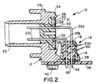
- Die cast housing 26 defines a rear face 34 thereof, with a plurality of mounting pins 36 projecting from the rear face for insertion into mounting holes 37 in flexible capacitor filter circuits 20 to mount the circuits to the rear of the housing and establish electrical contact between the housing and the flexible circuits.
- main connector 12 particularly die cast housing 26, is constructed to provide a right angle connector mountable to a printed circuit board 38, with terminals 22 extending through passageways 30 generally parallel to the printed circuit board.
- Appropriate fastening means 40 is provided for securing main connector 12, through its housing, to the printed circuit board in its right angle orientation.
- terminals 22 are bent at right angles, as at 22b, so that tail portions 22a of the terminals extend perpendicular to printed circuit board 38 for insertion into appropriate holes 42 in the circuit board for interconnection to appropriate circuit traces on the board or in the holes.
- the flat flexible circuit includes a flat dielectric substrate 45 which may be of various materials, but a polyamide material marketed by Du Pont Corporation under the trademark KAPTON has proven effective. Other materials, such as a polyester material marketed under the trademark MYLAR also could be used.
- Hole 37 may be provided as a prepunched, generally round hole for receiving a round pin such as pin 36.
- a ductile conductive film or flat conductor 44 is deposited on substrate 45 in an area at least about hole 37.
- the film 44 substantially covers dielectric substrate 45 (i.e. flat flexible circuit 20) and acts as a ground plane for the connector assembly.
- the film is of copper or like material and may be plated with a tin/lead alloy like material or precious metal.
- a conductive adhesive 46 is deposited on conductive film 44 over the area of the hole in substrate 45 of flat flexible circuit 20 or on the pin 36 and the area of the housing around the pin.
- the adhesive is an omni-directional adhesive (versus a "Z-axis" adhesive) and includes a nonconductive base or resin incorporating conductive particles therein. Since the adhesive is omni-directional, it is not limited in its areas of conductivity to points of pressure as in "Z-axis" adhesives. Therefore, the omni-directional adhesive expands the conductive interface between the metal pin/housing and the metal ground plane.
- the adhesive includes in excess of twenty-five percent by weight content of conductive particles.
- pin 36 and housing 26 being fabricated of a first metal material such as magnesium, aluminum and the like, and with conductive film 44 being fabricated of copper material with or without a tin/lead plating, a conductive interface is created between dissimilar metals.
- adhesives as "Z-axis" adhesives, in addition to being expensive, provide limited conductive areas restricted to points of sufficient pressure to "activate” the adhesive.
- the invention contemplates that adhesive 46 be an omni-directional adhesive.
- the conductive particles of the adhesive are abrasive grain-like particles that break through oxides formed on the surfaces of dissimilar metals at the conductive interface.
- a preferred composition of the particles is a nickel material.
- adhesive 46 extends radially outwardly of hole 37 and pin 36 along a portion 50 of the rear face 34 of housing 26.
- portion 50 of rear face 34 is juxtaposed against or over the ground plane defined by conductive film 44 of flat flexible circuit 20. Therefore, the conductive interface between the housing and the ground plane is considerably expanded beyond the interface defined solely by pin 36 within hole 37 of the flat flexible circuit. This is afforded by the omni-directional adhesive.
Landscapes
- Engineering & Computer Science (AREA)
- Manufacturing & Machinery (AREA)
- Microelectronics & Electronic Packaging (AREA)
- Metallurgy (AREA)
- Details Of Connecting Devices For Male And Female Coupling (AREA)
- Connections Effected By Soldering, Adhesion, Or Permanent Deformation (AREA)
- Adhesives Or Adhesive Processes (AREA)
Applications Claiming Priority (2)
| Application Number | Priority Date | Filing Date | Title |
|---|---|---|---|
| US08/192,086 US5456616A (en) | 1994-02-04 | 1994-02-04 | Electrical device employing a flat flexible circuit |
| US192086 | 1994-02-04 |
Publications (2)
| Publication Number | Publication Date |
|---|---|
| EP0666705A2 true EP0666705A2 (fr) | 1995-08-09 |
| EP0666705A3 EP0666705A3 (fr) | 1996-01-03 |
Family
ID=22708186
Family Applications (1)
| Application Number | Title | Priority Date | Filing Date |
|---|---|---|---|
| EP95101023A Withdrawn EP0666705A3 (fr) | 1994-02-04 | 1995-01-26 | Dispositif électrique utilisant un circuit flexible plat. |
Country Status (5)
| Country | Link |
|---|---|
| US (1) | US5456616A (fr) |
| EP (1) | EP0666705A3 (fr) |
| JP (1) | JP2835581B2 (fr) |
| KR (1) | KR0170026B1 (fr) |
| SG (1) | SG45310A1 (fr) |
Cited By (3)
| Publication number | Priority date | Publication date | Assignee | Title |
|---|---|---|---|---|
| GB2303258A (en) * | 1995-07-07 | 1997-02-12 | Harting Elektronik Gmbh | Shielded electrical connector |
| WO1998054796A1 (fr) * | 1997-05-30 | 1998-12-03 | The Whitaker Corporation | Procede d'application d'une protection anti-decharge electrique a un connecteur electrique blinde |
| EP2131269A4 (fr) * | 2007-03-26 | 2011-05-18 | Nissha Printing | Panneau de protection avec fonction d'entrée tactile d'une fenêtre d'affichage d'instrument électronique |
Families Citing this family (25)
| Publication number | Priority date | Publication date | Assignee | Title |
|---|---|---|---|---|
| US5779502A (en) * | 1995-06-06 | 1998-07-14 | Ast Research | Socket integrating high frequency capacitor assembly |
| US6000951A (en) * | 1997-03-18 | 1999-12-14 | Prince Corporation | Electrical ribbon wire connectors |
| US5981870A (en) * | 1997-05-15 | 1999-11-09 | Chrysler Corporation | Flexible circuit board interconnect with strain relief |
| US5924873A (en) * | 1997-05-15 | 1999-07-20 | Chrysler Corporation | Flexible circuit board interconnect with strain relief |
| US5917149A (en) * | 1997-05-15 | 1999-06-29 | Daimlerchrysler Corporation | Flexible circuit board interconnect with strain relief |
| CA2213590C (fr) * | 1997-08-21 | 2006-11-07 | Keith C. Carroll | Connecteur pour circuit flexible et methode pour la fabrication de celui-ci |
| US6086384A (en) * | 1997-08-22 | 2000-07-11 | Molex Incorporated | Method of fabricating electronic device employing a flat flexible circuit and including the device itself |
| US6723928B1 (en) | 1997-09-29 | 2004-04-20 | Molex Incorporated | Terminal pins mounted in flexible substrates |
| CA2217591C (fr) * | 1997-10-07 | 2003-07-29 | 700674 Ontario Limited, Doing Business As Carroll Associates | Dispositif d'essais sans fil |
| US6120306A (en) * | 1997-10-15 | 2000-09-19 | Berg Technology, Inc. | Cast coax header/socket connector system |
| EP0921596A1 (fr) | 1997-11-24 | 1999-06-09 | Molex Incorporated | Bornes à lames montables sur des substrats souples |
| US6030234A (en) * | 1998-01-23 | 2000-02-29 | Molex Incorporated | Terminal pins mounted in flexible substrates |
| USH1991H1 (en) * | 1999-07-01 | 2001-09-04 | Methode Electronics, Inc. | Clockspring using flexible printed wiring |
| FR2796765B1 (fr) | 1999-07-20 | 2001-10-05 | Fci France | Bande de supports de contacts et procede de detachement d'un contact maintenu sur cette bande |
| US6364711B1 (en) * | 2000-10-20 | 2002-04-02 | Molex Incorporated | Filtered electrical connector |
| DE20019524U1 (de) * | 2000-11-17 | 2001-03-29 | TRW Automotive Electronics & Components GmbH & Co. KG, 78315 Radolfzell | Gehäusesystem für sicherheitsrelevante Steuergeräte in Kraftfahrzeugen |
| US7165994B2 (en) * | 2001-05-23 | 2007-01-23 | Samtec, Inc. | Electrical connector having a ground plane with independently configurable contacts |
| US6739884B2 (en) * | 2001-05-23 | 2004-05-25 | Samtec, Inc. | Electrical connector having a ground plane with independently configurable contacts |
| US6623307B2 (en) * | 2001-11-08 | 2003-09-23 | Hon Hai Precision Ind. Co., Ltd. | High frequency modular jack connector |
| US7270575B2 (en) * | 2003-02-12 | 2007-09-18 | Amphenol Corporation | Circuit board and socket assembly |
| US7182644B2 (en) * | 2003-04-30 | 2007-02-27 | Hewlett-Packard Development Company, L.P. | Filtering electromagnetic interference from low frequency transmission lines at a device enclosure |
| US6837747B1 (en) | 2004-04-19 | 2005-01-04 | Itt Manufacturing Enterprises, Inc. | Filtered connector |
| JP2006049070A (ja) * | 2004-08-04 | 2006-02-16 | Denso Corp | コネクタ部材 |
| US7708566B2 (en) * | 2007-10-30 | 2010-05-04 | Hon Hai Precision Ind. Co., Ltd. | Electrical connector with integrated circuit bonded thereon |
| JP6055661B2 (ja) * | 2012-11-16 | 2016-12-27 | 日本オクラロ株式会社 | 光モジュール及び光送受信装置 |
Family Cites Families (15)
| Publication number | Priority date | Publication date | Assignee | Title |
|---|---|---|---|---|
| BE789365A (fr) * | 1971-09-30 | 1973-03-27 | Amp Inc | Connecteur electrique |
| US4024627A (en) * | 1974-04-29 | 1977-05-24 | Amp Incorporated | Package mounting of electronic chips, such as light emitting diodes |
| US4503611A (en) * | 1981-09-18 | 1985-03-12 | Molex Incorporated | Method of making a circuit assembly |
| US4489999A (en) * | 1983-02-15 | 1984-12-25 | Motorola, Inc. | Socket and flexible PC board assembly and method for making |
| GB2152060B (en) * | 1983-12-02 | 1987-05-13 | Osaka Soda Co Ltd | Electrically conductive adhesive composition |
| US4667401A (en) * | 1985-11-26 | 1987-05-26 | Clements James R | Method of making an electronic device using an uniaxial conductive adhesive |
| ES2008808A6 (es) * | 1988-08-09 | 1989-08-01 | Amp Espanola | Un conectador electrico del tipo de clavija destinado a empalmar alambres para un sistema de comunicacion. |
| JP2513930B2 (ja) * | 1989-10-12 | 1996-07-10 | シーメンス アクチエンゲゼルシヤフト | フィルタプラグコネクタ |
| US4970624A (en) * | 1990-01-22 | 1990-11-13 | Molex Incorporated | Electronic device employing a conductive adhesive |
| IL97425A (en) * | 1991-03-04 | 1995-01-24 | Cohen Amir | author |
| US5082457A (en) * | 1991-03-29 | 1992-01-21 | Cummins Electronics Company, Inc. | Filter electrical connector |
| US5141455A (en) * | 1991-04-08 | 1992-08-25 | Molex Incorporated | Mounting of electronic components on substrates |
| DE9107385U1 (de) * | 1991-06-14 | 1992-07-16 | Filtec Filtertechnologie für die Elektronikindustrie GmbH, 59557 Lippstadt | Mehrpoliger Steckverbinder für elektronische Signalleitungen |
| US5286221A (en) * | 1992-10-19 | 1994-02-15 | Molex Incorporated | Filtered electrical connector assembly |
| US5266054A (en) * | 1992-12-22 | 1993-11-30 | The Whitaker Corporation | Sealed and filtered header receptacle |
-
1994
- 1994-02-04 US US08/192,086 patent/US5456616A/en not_active Expired - Lifetime
-
1995
- 1995-01-26 EP EP95101023A patent/EP0666705A3/fr not_active Withdrawn
- 1995-01-26 SG SG1996003261A patent/SG45310A1/en unknown
- 1995-02-02 JP JP7037539A patent/JP2835581B2/ja not_active Expired - Fee Related
- 1995-02-03 KR KR1019950001897A patent/KR0170026B1/ko not_active Expired - Fee Related
Cited By (4)
| Publication number | Priority date | Publication date | Assignee | Title |
|---|---|---|---|---|
| GB2303258A (en) * | 1995-07-07 | 1997-02-12 | Harting Elektronik Gmbh | Shielded electrical connector |
| WO1998054796A1 (fr) * | 1997-05-30 | 1998-12-03 | The Whitaker Corporation | Procede d'application d'une protection anti-decharge electrique a un connecteur electrique blinde |
| US5897388A (en) * | 1997-05-30 | 1999-04-27 | The Whitaker Corporation | Method of applying ESD protection to a shielded electrical |
| EP2131269A4 (fr) * | 2007-03-26 | 2011-05-18 | Nissha Printing | Panneau de protection avec fonction d'entrée tactile d'une fenêtre d'affichage d'instrument électronique |
Also Published As
| Publication number | Publication date |
|---|---|
| KR950026062A (ko) | 1995-09-18 |
| JP2835581B2 (ja) | 1998-12-14 |
| JPH07235348A (ja) | 1995-09-05 |
| EP0666705A3 (fr) | 1996-01-03 |
| US5456616A (en) | 1995-10-10 |
| SG45310A1 (en) | 1998-01-16 |
| KR0170026B1 (ko) | 1999-03-30 |
Similar Documents
| Publication | Publication Date | Title |
|---|---|---|
| US5456616A (en) | Electrical device employing a flat flexible circuit | |
| JP3372042B2 (ja) | シールド付きコネクタとメッキ孔を有する基板との組立体 | |
| EP0653816B1 (fr) | Assemblage de connecteur électrique filtré | |
| EP0663705B1 (fr) | Assemblage d'un connecteur électrique à filtre | |
| US5624277A (en) | Filtered and shielded electrical connector using resilient electrically conductive member | |
| EP0476702B1 (fr) | Connecteur électrique contenant des composants et méthode de fabrication pour celui-ci | |
| US5681173A (en) | Method for enhancing the signal carrying capability of an electrical connector | |
| WO2002058191A3 (fr) | Connecteur electrique blinde | |
| EP0860038B1 (fr) | Connecteur filtre de circuit avec bati | |
| US6533588B1 (en) | Connector assembly for flexible circuits | |
| US6030234A (en) | Terminal pins mounted in flexible substrates | |
| KR20030091715A (ko) | 여과 및 차폐 전기커넥터 | |
| US6619984B2 (en) | Electrical connector having improved shielding | |
| US6086384A (en) | Method of fabricating electronic device employing a flat flexible circuit and including the device itself | |
| US5094629A (en) | Electrical connector containing components and method of making same | |
| EP0906005B1 (fr) | Broche de contact montée sur des substrats flexibles | |
| JP2003508936A (ja) | Emi抑制配線プレートを備えた電気部品の組立体及びその製造方法並びにemi抑制配線プレート | |
| JPH06177573A (ja) | Icカード | |
| JPH08330030A (ja) | コネクタ |
Legal Events
| Date | Code | Title | Description |
|---|---|---|---|
| PUAI | Public reference made under article 153(3) epc to a published international application that has entered the european phase |
Free format text: ORIGINAL CODE: 0009012 |
|
| AK | Designated contracting states |
Kind code of ref document: A2 Designated state(s): DE ES FR GB IT SE |
|
| PUAL | Search report despatched |
Free format text: ORIGINAL CODE: 0009013 |
|
| AK | Designated contracting states |
Kind code of ref document: A3 Designated state(s): DE ES FR GB IT SE |
|
| 17P | Request for examination filed |
Effective date: 19960622 |
|
| STAA | Information on the status of an ep patent application or granted ep patent |
Free format text: STATUS: THE APPLICATION IS DEEMED TO BE WITHDRAWN |
|
| 18D | Application deemed to be withdrawn |
Effective date: 20020801 |