EP0667583A1 - Système de calcul d'un bidimensionel discrète transformé du cosinus - Google Patents
Système de calcul d'un bidimensionel discrète transformé du cosinus Download PDFInfo
- Publication number
- EP0667583A1 EP0667583A1 EP94120916A EP94120916A EP0667583A1 EP 0667583 A1 EP0667583 A1 EP 0667583A1 EP 94120916 A EP94120916 A EP 94120916A EP 94120916 A EP94120916 A EP 94120916A EP 0667583 A1 EP0667583 A1 EP 0667583A1
- Authority
- EP
- European Patent Office
- Prior art keywords
- block
- idct
- blocks
- signal
- response
- Prior art date
- Legal status (The legal status is an assumption and is not a legal conclusion. Google has not performed a legal analysis and makes no representation as to the accuracy of the status listed.)
- Granted
Links
Images



Classifications
-
- G—PHYSICS
- G06—COMPUTING OR CALCULATING; COUNTING
- G06F—ELECTRIC DIGITAL DATA PROCESSING
- G06F17/00—Digital computing or data processing equipment or methods, specially adapted for specific functions
- G06F17/10—Complex mathematical operations
- G06F17/14—Fourier, Walsh or analogous domain transformations, e.g. Laplace, Hilbert, Karhunen-Loeve, transforms
- G06F17/147—Discrete orthonormal transforms, e.g. discrete cosine transform, discrete sine transform, and variations therefrom, e.g. modified discrete cosine transform, integer transforms approximating the discrete cosine transform
-
- G—PHYSICS
- G06—COMPUTING OR CALCULATING; COUNTING
- G06F—ELECTRIC DIGITAL DATA PROCESSING
- G06F17/00—Digital computing or data processing equipment or methods, specially adapted for specific functions
- G06F17/10—Complex mathematical operations
Definitions
- the present invention relates to a two-dimensional inverse discrete cosine transform(IDCT) apparatus for use in a digital image processing system; and, more particularly, to an IDCT apparatus capable of processing a transformed video signal consisting of blocks of video data and various time gaps intervening therebetween.
- IDCT two-dimensional inverse discrete cosine transform
- transmission of digitized video signals can deliver video images of a much higher quality than the transmission of analog signals.
- an image signal comprising a sequence of image "frames"
- a substantial amount of data is generated for transmission, especially in the case of a high definition television system. Since, however, the available frequency bandwidth of a conventional transmission channel is limited, in order to transmit the substantial amounts of digital data through the limited channel bandwidth, it is inevitable to compress or reduce the volume of the transmission data.
- the image signal can be normally compressed without seriously affecting its integrity because there usually exist certain correlationships or redundancies among some of the pixels in a single frame and also among those of neighboring frames. Accordingly, most of prior art image signal encoding methods employ various compression techniques(or coding methods) built on the idea of utilizing or truncating the redundancies.
- DCT Discrete Cosine Transform
- the DCT is employed with such other coding methods such Differential Pulse-Code Modulation-(DPCM) and motion compensated predictive coding which employs a motion estimation and prediction(see MPEG Video Simulation Model Three, International Organization for Standardization, Coded Representation of Picture and Audio Information, 1990, ISO-IEC/JTC1/SC2/WG8 MPEG 90/041 ).
- DPCM Differential Pulse-Code Modulation-
- motion compensated predictive coding which employs a motion estimation and prediction(see MPEG Video Simulation Model Three, International Organization for Standardization, Coded Representation of Picture and Audio Information, 1990, ISO-IEC/JTC1/SC2/WG8 MPEG 90/041 ).
- each frame of image signal is first divided into blocks, each of which comprising a predetermined number, e.g., 64, of pixel data, and is processed, e.g., discrete cosine transformed, on a block-by-block basis.
- the image signal is subject to further processing, e.g., motion estimation and prediction.
- An additional signal containing, e.g., information about the encoding process, may be inserted between certain two successive blocks.
- the encoded image signal is subject to further processing such as channel coding for the transmission thereof.
- an image signal received through a transmission channel is subject to a series of decoding processes including, e.g., channel decoding, variable length decoding, run-length decoding and inverse quantization before an IDCT operation may be performed.
- an input signal to an IDCT apparatus is a transformed video signal provided from, e.g., an inverse quantizer included in the image decoding system.
- the input signal may include a data signal which contains a plurality of blocks each of which has a predetermined number of transformed data which is fed to the IDCT apparatus at a constant rate.
- a number of time gaps of variable durations may be inserted between a corresponding number of two successive blocks, wherein each time gap corresponds to said each additional signal inserted at the encoder and its duration may depend on the system. Therefore, the data signal also includes a multiplicity of time gaps each of which is inserted between two successive blocks.
- information signals which are related to the timing of the data signal are also included in the input signal and provided to the IDCT apparatus.
- a common example of such signals is a block start signal which is activated during a first input cycle of each block.
- a conventional IDCT processor performs an IDCT operation on a block-by-block basis, and, therefore, may have some constraints on the format or timing of the input.
- the transformed data should be applied to the IDCT processor sequentially at a constant rate of one input data per one clock cycle and the time gap should satisfy certain conditions.
- the time gap should be multiples of the number of input data in a block of clock cycles or should be greater than a latency.
- the latency as used herein refers to a time interval between the start of a block input and the start of its output and is defined by the characteristics of the IDCT processor.
- the IDCT processor of the art may become unable to deal with the time gaps of variable durations inserted between certain blocks.
- an IDCT apparatus for performing a two-dimensional IDCT operation on an input signal having a data signal and an information signal to generate an inverse transformed data signal, wherein said data signal includes a plurality of blocks of transformed coefficients and a multiplicity of time gaps of variable durations, each of said blocks having a multiple number of transformed coefficients and each of said time gaps being inserted between two successive blocks and said information signal includes a plurality of block start signals, each of which indicates the start of each block, comprising:
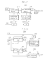
- the IDCT apparatus 1 comprises a 1st 1-D (one- dimensional) IDCT block 100 for performing a 1-D IDCT on a block of input data to thereby provide an intermediate block, a transposition memory block 300 for storing and transposing the intermediate block and a 2nd 1-D IDCT block 200 for subjecting the transposed intermediate block to another 1-D IDCT.
- a 1st 1-D (one- dimensional) IDCT block 100 for performing a 1-D IDCT on a block of input data to thereby provide an intermediate block
- a transposition memory block 300 for storing and transposing the intermediate block
- 2nd 1-D IDCT block 200 for subjecting the transposed intermediate block to another 1-D IDCT.
- An input signal to the IDCT apparatus 1 of the present invention is of a standard type transformed video signal which may be provided from another part of an image decoding system such as the inverse quantizer(not shown) and comprises a data signal and a block start signal.
- the data signal represented in Figs. 1 and Fig. 5 as INPUT DATA includes a plurality of blocks of transformed data and the block start signal represented as DBS denotes a start of each block included in the data signal.
- Each of the blocks has a predetermined number, e.g., 64, of transformed data and for some of the two successive blocks, a time gap of variable duration is inserted therebetween. For example, a time gap of duration G is inserted between second and third blocks in Fig. 5.
- the data signal is inputted to the 1st 1-D IDCT block 100 to be 1-D inverse transformed therein.
- the 1st 1-D IDCT block 100 performs the 1-D IDCT by multiplying a predetermined IDCT coefficient matrix to an input block, thereby providing an intermediate block as will be explained in accordance with Fig. 2.
- the intermediate block provided from the 1 st 1-D IDCT block 100 is transposed in the transposition memory block 300 to be coupled to the 2nd 1-D IDCT block 200.
- the operation of the 2nd 1-D IDCT block 200 is substantially the same with that of the 1st 1-D IDCT block 100 except that it multiplies IDCT coefficient matrix to the transposed intermediate block instead of the input block. That is, the transposed intermediate block inputted from the transposition memory block 300 is 1-D inverse transformed at the 2nd 1-D IDCT block 200 to form a 2-D inverse transformed block.
- the 2-D inverse transformed block is provided to anther part of the decoding system such as motion compensator.
- the block start signal is also inputted to each block included in the IDCT apparatus 1 for controlling each of the blocks as will be explained hereinafter.
- the 1st 1-D IDCT block 100 includes a multiplication block 110 for multiplying each of the IDCT coefficients included in the IDCT coefficient matrix with each input data, an accumulation block 120 for adding a predetermined number, e.g., 8, of products provided from the multiplication block 110 to form a 1-D inverse transformed data included in the intermediate block, a coefficient generator 115 for providing proper IDCT coefficients used in the multiplication block 110 and an accumulation controller 125 for generating control signals used in the accumulation block 120.
- a multiplication block 110 for multiplying each of the IDCT coefficients included in the IDCT coefficient matrix with each input data
- an accumulation block 120 for adding a predetermined number, e.g., 8, of products provided from the multiplication block 110 to form a 1-D inverse transformed data included in the intermediate block
- a coefficient generator 115 for providing proper IDCT coefficients used in the multiplication block 110
- an accumulation controller 125 for generating control signals used in the accumulation block 120.
- the 1st 1-D IDCT block 100 also includes delay blocks D1 117 and D2 127 for providing DBS1 and DBS2 which are delayed block start signals by predetermined intervals.
- DBS1 and DBS2 are used in the coefficient generator 115 and the accumulation controller 125, respectively, for the timing control of the multiplication block 110 and the accumulation block 120.
- DBS is delayed by a predetermined interval T1 and then again by T2 to form DBS1 and DBS2, respectively, wherein T1 denotes a time interval between a start of input block and a start of coefficient input to the multiplication block 110. Therefore, the coefficient generator 115 starts to provide IDCT coefficients to the multiplication block 110 in response to DBS1. In other words, the operation of the coefficient generator 115 and the multiplication block 110 is controlled by DBS1.
- T2 denotes a time interval between a start of coefficient input to the multiplication block 110 and a start of product input from the multiplication block 110 to the accumulation block 120.
- the contents of the accumulation block 120 is cleared and accumulation operation for the products of a new input block is performed from then on. Therefore, the operation of the accumulation block 120 and the accumulation controller 125 is controlled by DBS2.
- T1 and T2 are predetermined according to a system design. By the operation of the multiplication block 110 and the accumulation block 120, each of the input block is 1-D inverse transformed in the 1st 1-D IDCT 100 to form an intermediate block and coupled to the transposition memory block 300 on line 150.
- the transposition memory block 300 includes two 8x8 transposition RAMs (Random Access Memories) 310 and 320 for storing the intermediate blocks alternately, a transposition memory controller 330 for generating various control signals for the writing and read operation of the two transposition RAMs 310 and 320 and a multiplexor 350 for selecting an output from one of the transposition RAMs and providing it to the 2nd 1-D IDCT block 200. It also includes a delay block D3 335 for providing DBS3. As shown in Fig.
- DBS3 is produced by delaying DBS by a predetermined time (T1 + T2 + T3), wherein (T1 + T2 + T3) denotes an interval between the start of an input block to the 1st 1-D IDCT block 100 and the start of the output of the corresponding intermediate block from the 1st 1-D IDCT block 100.
- the intermediate blocks provided from the 1 st 1-D IDCT block 100 on the line 150 are stored in the two transposition RAMs 310 and 320, alternately. That is, two neighboring blocks are stored in two different transposition RAMs. For example, if the 1 st intermediate block shown in Fig. 5 is stored in the transposition RAM 310, the 2nd intermediate block is stored in the transposition RAM 320. By storing intermediate blocks in this manner, an intermediate block stored at one of the transposition RAMs can be provided in a transposed sequence to the 2nd 1-D IDCT block 200 while another intermediate block is being stored in the other transposition RAM.
- AD1 and AD2 are address signals for the read and write operation of the two transposition RAMs 310 and 320 and the write/read selection signals W/R1 and W/R2 determine the operation of the transposition RAMs 310 and 320, respectively.
- the transposition RAMs 310 and 320 are controlled so that only one of the transposition RAMs performs the read operation while the other one is doing the write operation.
- transposition RAMs are stored at one of the transposition RAMs and provided to the multiplexor 350 in a transposed sequence.
- a 1 st or 3rd intermediate block is stored in the transposition RAM 310; and a 2nd or 4th intermediate block is stored in the transposition RAM 320. While the 2nd intermediate block is stored in the transposition RAM 320, the transposed 1 st intermediate block is provided to the multiplexor 350. From the waveform of the intermediate block and the transposed intermediate block shown in Fig. 5, it can be easily seen that the transposed 2nd intermediate block is retrieved from the transposition RAM 320 as soon as it is stored therein.
- the transposed 2nd intermediate block is retrieved from the second transposition RAM 320.
- invalid data corresponding to the time gap G" is retrieved from the transposition RAM 320 as shown in Fig. 5.
- the multiplexor 350 selects transposed data provided by the read operation of one of the transposition RAMs in response to the selection signal provided from the transposition memory controller 330 on a line 340.
- W/R2 can be used as the selection signal wherein the output from the transposition RAM 310 is selected when W/R2 is active; and the output from the transposition RAM 320 is selected when W/R1 is active.
- the transposed intermediate block provided from the multiplexor 350 is inputted to the 2nd 1-D IDCT block 200.
- the input to the 2nd 1-D IDCT block also includes a time gap between 2nd and 3rd intermediate blocks as shown in Fig. 5.
- the 2nd IDCT block 200 performs substantially the same operation as that of the 1st 1-D IDCT block 100.
- FIG. 4 there is a detailed block diagram of the transposition memory controller 330 shown in Fig. 3.
- the transposition memory controller 330 generates address signals, write/read selection signals for the two transposition RAMs 310 and 320 and the selection signal for the multiplexor 350.
- the transposition memory controller 330 includes a demultiplexor 10 for dividing DBS3 to DBS30 and DBS3E shown in Fig. 5 and a first and a second address generating blocks 50 and 60 for generating address signals AD1 and AD2 and write/read selection signals W/R1 and W/R2 for the transposition RAMs 310 and 320 in response to DBS30 and DBS3E, respectively.
- DBS30 indicates the start of each odd-numbered intermediate block while DBS3E denotes the start of each even-numbered intermediate block.
- the first address generating block 50 includes an address generator 15 that generates a sequence of predetermined write addresses, e.g., 0 to 63, twice for the 128 clock cycles from the rising edge of DBS30.
- the write address sequence is converted to a read address sequence in an address transpose block 25 for the retrieval of the transposed intermediate block from the transposition RAM 310.
- One of the write and read address sequences is selected in a multiplexor 35 to form the address signal AD1 and fed to the transposition RAM 310.
- the write address sequence is selected and the first intermediate block is written to the transposition RAM 310 as shown in the 6th row in Fig. 5.
- the read address sequence from the address transpose block 25 is selected for 64 clock cycles and the transposed first intermediate block is retrieved from the transposition RAM 310 as depicted in the last row of Fig 5.
- the write/read selection signal as well as the address signal is needed. Therefore, the first address generating block 50 also generates the write/read selection signal W/R1 for the transposition RAM 310.
- the transposition RAM 310 performs a write or a read operation when W/R1 shown in Fig. 5 is "1 or "0", respectively.
- the second address generating block 60 performs the same operation as that of the first address generating block 50 except that it generates an address signal for 128 clock cycles from the rising edge of DBS3E. Specifically, in response to the first rising edge of DBS3E shown in Fig. 5, the second address generating block 60 generates a predetermined write and read address sequence for the storing and retrieving of the second intermediate block. The second address generating block 60 also generates the write/read selection signal W/R2 for the transposition RAM 320, wherein a write or a read operation is performed when W/R2 shown in Fig. 5 is "1 " or "0", respectively.
- the data signal represented as INPUT DATA includes a plurality of blocks of transformed data and a time gap G is inserted between a second and a third blocks.
- the 1st 1-D IDCT block 100 shown in Fig. 1 performs the 1-D IDCT operation in response to DBS1 and DBS2 and generates the intermediate block shown in Fig. 5.
- the input data includes a time gap G between the 2nd and the 3rd block, a time gap G' of same duration exists between the 2nd and the 3rd intermediate blocks as shown in Fig. 5.
- DBS30 and DBS3E denote start of odd-numbered and even-numbered intermediate blocks, respectively.
- the odd-numbered and the even-numbered intermediate blocks are stored in the transposition memory block 300 shown in Fig. 1 when W/R1 and W/R2 are "1 ", respectively.
- the intermediate blocks are retrieved in a transposed sequence when the corresponding write/read selection signal is "0" as shown in the last line of Fig. 5, and provided to the 2nd 1-D IDCT block 200.
- invalid data is provided to the 2nd 1-D IDCT block 200 during the time gap denoted as G".
- the 2nd 1-D IDCT block 200 deals with the time gap as explained in reference to Fig. 2.
- the 2nd 1-D IDCT block 200 shown in Fig. 2 performs the same operation as the 1st 1-D IDCT block 100 as explained in reference to Figs. 2 and 5 and provides 2-D inverse transformed data to other parts of the decoding system.
Landscapes
- Physics & Mathematics (AREA)
- Engineering & Computer Science (AREA)
- General Physics & Mathematics (AREA)
- Mathematical Physics (AREA)
- Theoretical Computer Science (AREA)
- Data Mining & Analysis (AREA)
- Mathematical Analysis (AREA)
- Pure & Applied Mathematics (AREA)
- Mathematical Optimization (AREA)
- Computational Mathematics (AREA)
- Algebra (AREA)
- Databases & Information Systems (AREA)
- Software Systems (AREA)
- General Engineering & Computer Science (AREA)
- Discrete Mathematics (AREA)
- Compression Or Coding Systems Of Tv Signals (AREA)
- Compression, Expansion, Code Conversion, And Decoders (AREA)
- Compression Of Band Width Or Redundancy In Fax (AREA)
- Complex Calculations (AREA)
Applications Claiming Priority (2)
| Application Number | Priority Date | Filing Date | Title |
|---|---|---|---|
| KR1019940000751A KR0130446B1 (ko) | 1994-01-18 | 1994-01-18 | 이차원 역이산코사인 변환방법 및 장치 |
| KR9400751 | 1994-01-18 |
Publications (2)
| Publication Number | Publication Date |
|---|---|
| EP0667583A1 true EP0667583A1 (fr) | 1995-08-16 |
| EP0667583B1 EP0667583B1 (fr) | 1999-03-17 |
Family
ID=19375766
Family Applications (1)
| Application Number | Title | Priority Date | Filing Date |
|---|---|---|---|
| EP94120916A Expired - Lifetime EP0667583B1 (fr) | 1994-01-18 | 1994-12-29 | Système de calcul d'une transformée en cosinus discret bidimensionnelle |
Country Status (5)
| Country | Link |
|---|---|
| EP (1) | EP0667583B1 (fr) |
| JP (1) | JPH0844709A (fr) |
| KR (1) | KR0130446B1 (fr) |
| CN (1) | CN1117175A (fr) |
| DE (1) | DE69417208T2 (fr) |
Cited By (2)
| Publication number | Priority date | Publication date | Assignee | Title |
|---|---|---|---|---|
| EP0809193A3 (fr) * | 1996-05-20 | 1999-10-20 | Matsushita Electric Industrial Co., Ltd. | Processeur de transformation orthogonale |
| WO2001026056A1 (fr) * | 1999-10-01 | 2001-04-12 | Koninklijke Philips Electronics N.V. | Rangement et extraction de donnees |
Families Citing this family (2)
| Publication number | Priority date | Publication date | Assignee | Title |
|---|---|---|---|---|
| JPH10341438A (ja) | 1997-06-09 | 1998-12-22 | Sharp Corp | 画像処理装置 |
| JP4536109B2 (ja) * | 2007-12-26 | 2010-09-01 | 富士通株式会社 | 半導体装置および信号処理方法 |
Citations (4)
| Publication number | Priority date | Publication date | Assignee | Title |
|---|---|---|---|---|
| WO1988007725A1 (fr) * | 1987-03-24 | 1988-10-06 | Bell Communications Research, Inc. | Processeur permettant d'obtenir des transformees de cosinus discretes bidimensionnelles |
| EP0366976A2 (fr) * | 1988-11-03 | 1990-05-09 | Robert Bosch Gmbh | Circuit pour transformée |
| EP0566184A2 (fr) * | 1992-04-13 | 1993-10-20 | Koninklijke Philips Electronics N.V. | Transformateur d'image ainsi que système de télévision comportant un émetteur et un récepteur munis d'un transformateur |
| EP0572766A2 (fr) * | 1992-06-04 | 1993-12-08 | International Business Machines Corporation | Architecture à tâche pipe-line pour le traitement d'image vidéo |
-
1994
- 1994-01-18 KR KR1019940000751A patent/KR0130446B1/ko not_active Expired - Fee Related
- 1994-12-28 JP JP6338810A patent/JPH0844709A/ja active Pending
- 1994-12-29 DE DE69417208T patent/DE69417208T2/de not_active Expired - Fee Related
- 1994-12-29 EP EP94120916A patent/EP0667583B1/fr not_active Expired - Lifetime
-
1995
- 1995-01-16 CN CN95101261A patent/CN1117175A/zh active Pending
Patent Citations (4)
| Publication number | Priority date | Publication date | Assignee | Title |
|---|---|---|---|---|
| WO1988007725A1 (fr) * | 1987-03-24 | 1988-10-06 | Bell Communications Research, Inc. | Processeur permettant d'obtenir des transformees de cosinus discretes bidimensionnelles |
| EP0366976A2 (fr) * | 1988-11-03 | 1990-05-09 | Robert Bosch Gmbh | Circuit pour transformée |
| EP0566184A2 (fr) * | 1992-04-13 | 1993-10-20 | Koninklijke Philips Electronics N.V. | Transformateur d'image ainsi que système de télévision comportant un émetteur et un récepteur munis d'un transformateur |
| EP0572766A2 (fr) * | 1992-06-04 | 1993-12-08 | International Business Machines Corporation | Architecture à tâche pipe-line pour le traitement d'image vidéo |
Non-Patent Citations (1)
| Title |
|---|
| P.DUHAMEL ET AL: "A DCT chip based on a new structured and computationally efficient DCT algorithm", PROCEEDINGS OF THE 1990 IEEE INTERNATIONAL SYMPOSIUM ON CIRCUITS AND SYSTEMS, IEEE PRESS NEW YORK US, vol. 1/4, 1 May 1990 (1990-05-01), NEW ORLEANS, US, pages 77 - 80, XP000166727 * |
Cited By (3)
| Publication number | Priority date | Publication date | Assignee | Title |
|---|---|---|---|---|
| EP0809193A3 (fr) * | 1996-05-20 | 1999-10-20 | Matsushita Electric Industrial Co., Ltd. | Processeur de transformation orthogonale |
| US6282555B1 (en) | 1996-05-20 | 2001-08-28 | Matsushita Electric Industrial Co., Ltd. | Orthogonal transform processor |
| WO2001026056A1 (fr) * | 1999-10-01 | 2001-04-12 | Koninklijke Philips Electronics N.V. | Rangement et extraction de donnees |
Also Published As
| Publication number | Publication date |
|---|---|
| CN1117175A (zh) | 1996-02-21 |
| DE69417208T2 (de) | 1999-07-08 |
| KR0130446B1 (ko) | 1998-04-15 |
| KR950024094A (ko) | 1995-08-21 |
| EP0667583B1 (fr) | 1999-03-17 |
| DE69417208D1 (de) | 1999-04-22 |
| JPH0844709A (ja) | 1996-02-16 |
Similar Documents
| Publication | Publication Date | Title |
|---|---|---|
| EP0431319B1 (fr) | Dispositif de codage d'un signal vidéo, méthode de codage et système de transmission d'un signal vidéo | |
| US7646813B2 (en) | Encoding circuit for transform coding of a picture signal and decoding circuit for decoding said signal | |
| EP0519962B1 (fr) | Codage d'image numerique utilisant une analyse aleatoire de trames image | |
| US5253078A (en) | System for compression and decompression of video data using discrete cosine transform and coding techniques | |
| US5646687A (en) | Temporally-pipelined predictive encoder/decoder circuit and method | |
| US6211864B1 (en) | Method and apparatus for optimizing storage of compressed images in memory | |
| US5910824A (en) | Frame memory for a motion picture decoder | |
| EP0565223A2 (fr) | Procédé de compression d'un signal d'image numérique avec ordonnement et formattage des données codées et restitution d'images partielles à partir des données | |
| CN1058689A (zh) | 使用前馈量化估计器的数据压缩 | |
| US5552829A (en) | Image signal coding system | |
| EP0765090A3 (fr) | Appareil et procédé de codage et enregistrement/reproduction d'image | |
| EP0736843A2 (fr) | Système de compression d'images vidéo animées avec quantification adaptive | |
| KR100267125B1 (ko) | 압축 디지탈 비디오 시퀀스 복호화 및 디스플레이 방법과 압축 디지탈 비디오 정보 복호화 장치 | |
| EP0667583B1 (fr) | Système de calcul d'une transformée en cosinus discret bidimensionnelle | |
| US5519648A (en) | Inverse discrete cosine transformer | |
| EP0566184A2 (fr) | Transformateur d'image ainsi que système de télévision comportant un émetteur et un récepteur munis d'un transformateur | |
| EP0732671B1 (fr) | Système de décodage vidéo | |
| EP0776133A2 (fr) | Décodeur de signal d'image | |
| US5703647A (en) | Apparatus for encoding/decoding a video signal | |
| US6504871B1 (en) | IDCT processor for use in decoding MPEG compliant video bitstreams meeting 2-frame and letterboxing requirements | |
| JPS62284535A (ja) | ブロツクリスト変換を用いたデ−タ符号化方法および符号化装置 | |
| US5774590A (en) | Image data reproducing apparatus | |
| JP2830184B2 (ja) | 映像信号符号化装置及び映像信号符号化方法 | |
| JP2934425B1 (ja) | 画像データ圧縮装置および画像データ伸長装置 | |
| JPH0738894A (ja) | 画像符号化装置 |
Legal Events
| Date | Code | Title | Description |
|---|---|---|---|
| PUAI | Public reference made under article 153(3) epc to a published international application that has entered the european phase |
Free format text: ORIGINAL CODE: 0009012 |
|
| AK | Designated contracting states |
Kind code of ref document: A1 Designated state(s): DE FR GB NL |
|
| 17P | Request for examination filed |
Effective date: 19960214 |
|
| GRAG | Despatch of communication of intention to grant |
Free format text: ORIGINAL CODE: EPIDOS AGRA |
|
| 17Q | First examination report despatched |
Effective date: 19980206 |
|
| GRAG | Despatch of communication of intention to grant |
Free format text: ORIGINAL CODE: EPIDOS AGRA |
|
| GRAH | Despatch of communication of intention to grant a patent |
Free format text: ORIGINAL CODE: EPIDOS IGRA |
|
| GRAH | Despatch of communication of intention to grant a patent |
Free format text: ORIGINAL CODE: EPIDOS IGRA |
|
| GRAA | (expected) grant |
Free format text: ORIGINAL CODE: 0009210 |
|
| AK | Designated contracting states |
Kind code of ref document: B1 Designated state(s): DE FR GB NL |
|
| PG25 | Lapsed in a contracting state [announced via postgrant information from national office to epo] |
Ref country code: FR Free format text: LAPSE BECAUSE OF FAILURE TO SUBMIT A TRANSLATION OF THE DESCRIPTION OR TO PAY THE FEE WITHIN THE PRESCRIBED TIME-LIMIT Effective date: 19990317 |
|
| REF | Corresponds to: |
Ref document number: 69417208 Country of ref document: DE Date of ref document: 19990422 |
|
| EN | Fr: translation not filed | ||
| PGFP | Annual fee paid to national office [announced via postgrant information from national office to epo] |
Ref country code: NL Payment date: 19991228 Year of fee payment: 6 |
|
| PGFP | Annual fee paid to national office [announced via postgrant information from national office to epo] |
Ref country code: GB Payment date: 19991229 Year of fee payment: 6 |
|
| PLBE | No opposition filed within time limit |
Free format text: ORIGINAL CODE: 0009261 |
|
| STAA | Information on the status of an ep patent application or granted ep patent |
Free format text: STATUS: NO OPPOSITION FILED WITHIN TIME LIMIT |
|
| 26N | No opposition filed | ||
| PG25 | Lapsed in a contracting state [announced via postgrant information from national office to epo] |
Ref country code: DE Free format text: LAPSE BECAUSE OF NON-PAYMENT OF DUE FEES Effective date: 20001003 |
|
| PG25 | Lapsed in a contracting state [announced via postgrant information from national office to epo] |
Ref country code: GB Free format text: LAPSE BECAUSE OF NON-PAYMENT OF DUE FEES Effective date: 20001229 |
|
| PG25 | Lapsed in a contracting state [announced via postgrant information from national office to epo] |
Ref country code: NL Free format text: LAPSE BECAUSE OF NON-PAYMENT OF DUE FEES Effective date: 20010701 |
|
| GBPC | Gb: european patent ceased through non-payment of renewal fee |
Effective date: 20001229 |
|
| NLV4 | Nl: lapsed or anulled due to non-payment of the annual fee |
Effective date: 20010701 |