EP0667734A1 - Ballast électronique pour lampe fluorescente avec circuit oscillant pour limiter le facteur de forme et corriger le facteur de puissance - Google Patents
Ballast électronique pour lampe fluorescente avec circuit oscillant pour limiter le facteur de forme et corriger le facteur de puissance Download PDFInfo
- Publication number
- EP0667734A1 EP0667734A1 EP94830048A EP94830048A EP0667734A1 EP 0667734 A1 EP0667734 A1 EP 0667734A1 EP 94830048 A EP94830048 A EP 94830048A EP 94830048 A EP94830048 A EP 94830048A EP 0667734 A1 EP0667734 A1 EP 0667734A1
- Authority
- EP
- European Patent Office
- Prior art keywords
- bridge
- circuit
- lamp
- current
- resonant circuit
- Prior art date
- Legal status (The legal status is an assumption and is not a legal conclusion. Google has not performed a legal analysis and makes no representation as to the accuracy of the status listed.)
- Granted
Links
- 239000003990 capacitor Substances 0.000 claims description 21
- 238000009499 grossing Methods 0.000 claims description 7
- 230000005294 ferromagnetic effect Effects 0.000 claims description 6
- 238000004804 winding Methods 0.000 claims description 5
- 230000001939 inductive effect Effects 0.000 claims 1
- 230000000087 stabilizing effect Effects 0.000 description 2
- 238000010586 diagram Methods 0.000 description 1
- 230000010355 oscillation Effects 0.000 description 1
Images



Classifications
-
- H—ELECTRICITY
- H02—GENERATION; CONVERSION OR DISTRIBUTION OF ELECTRIC POWER
- H02M—APPARATUS FOR CONVERSION BETWEEN AC AND AC, BETWEEN AC AND DC, OR BETWEEN DC AND DC, AND FOR USE WITH MAINS OR SIMILAR POWER SUPPLY SYSTEMS; CONVERSION OF DC OR AC INPUT POWER INTO SURGE OUTPUT POWER; CONTROL OR REGULATION THEREOF
- H02M1/00—Details of apparatus for conversion
- H02M1/42—Circuits or arrangements for compensating for or adjusting power factor in converters or inverters
- H02M1/4208—Arrangements for improving power factor of AC input
- H02M1/4241—Arrangements for improving power factor of AC input using a resonant converter
-
- H—ELECTRICITY
- H02—GENERATION; CONVERSION OR DISTRIBUTION OF ELECTRIC POWER
- H02M—APPARATUS FOR CONVERSION BETWEEN AC AND AC, BETWEEN AC AND DC, OR BETWEEN DC AND DC, AND FOR USE WITH MAINS OR SIMILAR POWER SUPPLY SYSTEMS; CONVERSION OF DC OR AC INPUT POWER INTO SURGE OUTPUT POWER; CONTROL OR REGULATION THEREOF
- H02M1/00—Details of apparatus for conversion
- H02M1/42—Circuits or arrangements for compensating for or adjusting power factor in converters or inverters
- H02M1/4208—Arrangements for improving power factor of AC input
- H02M1/425—Arrangements for improving power factor of AC input using a single converter stage both for correction of AC input power factor and generation of a high frequency AC output voltage
-
- H—ELECTRICITY
- H02—GENERATION; CONVERSION OR DISTRIBUTION OF ELECTRIC POWER
- H02M—APPARATUS FOR CONVERSION BETWEEN AC AND AC, BETWEEN AC AND DC, OR BETWEEN DC AND DC, AND FOR USE WITH MAINS OR SIMILAR POWER SUPPLY SYSTEMS; CONVERSION OF DC OR AC INPUT POWER INTO SURGE OUTPUT POWER; CONTROL OR REGULATION THEREOF
- H02M7/00—Conversion of AC power input into DC power output; Conversion of DC power input into AC power output
- H02M7/42—Conversion of DC power input into AC power output without possibility of reversal
- H02M7/44—Conversion of DC power input into AC power output without possibility of reversal by static converters
- H02M7/48—Conversion of DC power input into AC power output without possibility of reversal by static converters using discharge tubes with control electrode or semiconductor devices with control electrode
- H02M7/53—Conversion of DC power input into AC power output without possibility of reversal by static converters using discharge tubes with control electrode or semiconductor devices with control electrode using devices of a triode or transistor type requiring continuous application of a control signal
- H02M7/537—Conversion of DC power input into AC power output without possibility of reversal by static converters using discharge tubes with control electrode or semiconductor devices with control electrode using devices of a triode or transistor type requiring continuous application of a control signal using semiconductor devices only, e.g. single switched pulse inverters
- H02M7/538—Conversion of DC power input into AC power output without possibility of reversal by static converters using discharge tubes with control electrode or semiconductor devices with control electrode using devices of a triode or transistor type requiring continuous application of a control signal using semiconductor devices only, e.g. single switched pulse inverters in a push-pull configuration
-
- H—ELECTRICITY
- H05—ELECTRIC TECHNIQUES NOT OTHERWISE PROVIDED FOR
- H05B—ELECTRIC HEATING; ELECTRIC LIGHT SOURCES NOT OTHERWISE PROVIDED FOR; CIRCUIT ARRANGEMENTS FOR ELECTRIC LIGHT SOURCES, IN GENERAL
- H05B41/00—Circuit arrangements or apparatus for igniting or operating discharge lamps
- H05B41/14—Circuit arrangements
- H05B41/26—Circuit arrangements in which the lamp is fed by power derived from DC by means of a converter, e.g. by high-voltage DC
- H05B41/28—Circuit arrangements in which the lamp is fed by power derived from DC by means of a converter, e.g. by high-voltage DC using static converters
-
- Y—GENERAL TAGGING OF NEW TECHNOLOGICAL DEVELOPMENTS; GENERAL TAGGING OF CROSS-SECTIONAL TECHNOLOGIES SPANNING OVER SEVERAL SECTIONS OF THE IPC; TECHNICAL SUBJECTS COVERED BY FORMER USPC CROSS-REFERENCE ART COLLECTIONS [XRACs] AND DIGESTS
- Y02—TECHNOLOGIES OR APPLICATIONS FOR MITIGATION OR ADAPTATION AGAINST CLIMATE CHANGE
- Y02B—CLIMATE CHANGE MITIGATION TECHNOLOGIES RELATED TO BUILDINGS, e.g. HOUSING, HOUSE APPLIANCES OR RELATED END-USER APPLICATIONS
- Y02B70/00—Technologies for an efficient end-user side electric power management and consumption
- Y02B70/10—Technologies improving the efficiency by using switched-mode power supplies [SMPS], i.e. efficient power electronics conversion e.g. power factor correction or reduction of losses in power supplies or efficient standby modes
Definitions
- the invention relates to an electronic reactor or ballast for one or more discharge lamps of the type indicated in the introductory part of Claim 1.
- the electronic reactor generally has an input section consisting of a low-pass filter and a diode bridge, which has the function of rectifying the alternating mains voltage to supply it to a power oscillator in which the direct voltage is transformed into high-frequency alternating voltage and is then transferred to the resonant circuit comprising the lamp.
- the supply voltage across the terminals of the load circuit is a square-wave voltage at a high frequency, typically of the order of 25-30 kHz. It is supplied to a load circuit which typically has at least one discharge lamp with a capacitor in parallel and a stabilizing inductance in series.
- a capacitor is also provided, in series with the load circuit, enabling the power factor to be corrected.
- the amplitude of the current and voltage across the lamp terminals fluctuate at low frequency, typically at twice the mains frequency. This phenomenon is known as "ripple". The extent of this fluctuation is characterized by what is known as a crest factor. The fluctuation of the maximum value of the current amplitude in the lamp is extremely harmful, since it curtails the mean service life of the lamp.
- the object of the present invention is to propose an improvement to the common electrical reactor which enables the ripple phenomenon to be reduced drastically, if not completely eliminated.
- the invention provides an auxiliary series resonant circuit connected between the output of the lamp supply half-bridge and the bridge rectifier.
- This auxiliary resonant circuit stores and returns power with each switching cycle of the switch means of the load circuit supply half-bridge. The oscillation of the maximum current intensity in the load circuit is therefore reduced, and consequently the crest factor is reduced.
- the auxiliary series resonant circuit is a circuit of the LC type, with one inductance and one capacitor, and is connected between the output of the half-bridge and the positive pole of the rectifier.
- the inductance of the auxiliary resonant circuit and the inductance of the load circuit may be wound on a common ferromagnetic core advantageously consisting (in a preferred embodiment) of a three- column core with two air gaps on the two outer columns on which the two windings are made.
- the auxiliary resonant circuit also simultaneously corrects the power factor.
- the auxiliary resonant circuit it is possible to obtain, for the same value of the smoothing capacitor, a much smaller crest factor than in conventional reactors.
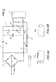
- the circuit has a filter 1, at whose input there is an alternating voltage supplied from a source indicated schematically by 3.
- the filter output is connected to a diode bridge rectifier indicated by 5.
- Two lines 7 and 9, positive and negative respectively, are connected to the positive pole 5A and the negative pole 5B of the bridge rectifier 5.
- the direct voltage supplied by the bridge rectifier 5 is transformed to alternating voltage at high frequency by two switches 11 and 13, suitably controlled by an electronic control circuit 15, of a type known in itself and not described in greater detail.
- the load supply voltage is obtained by alternate switching of the two switches 11 and 13.
- the load circuit is connected between the output 19 of the half-bridge formed by the switches 11 and 13 and the negative line 9, but could also be connected between the said output 19 and the positive line 7.
- the load circuit comprises a discharge lamp L in parallel with a capacitor 21.
- An inductance 23, consisting of a stabilizing coil, and a capacitor 20 are connected in series with the lamp L and the capacitor 21.
- the load circuit could also comprise two or more lamps with corresponding capacitors and inductances, in series and in parallel respectively.
- Two diodes 25 and 27 are connected in parallel with the two switches 11 and 13 respectively of the supply half-bridge of the load circuit.
- a smoothing capacitor 29 is also connected in parallel with the half-bridge between the negative line 9 and the positive line 7 down-line from a diode 31.
- An auxiliary series resonant circuit indicated in a general way by 33 and comprising an inductance 35 and a capacitor 37 is connected between the output 19 of the half-bridge formed by the switches 11 and 13 and the positive pole 5A of the bridge rectifier 5.
- the four phases of each switching cycle of the circuit described above will now be described with reference to Figs. 2 to 5 and 6A to 6D.
- the load current variation shown in Figs. 6A - 6D is intended to relate to a cycle which is repeated with a frequency of 25-30 kHz, while the input voltage of the bridge 5 varies sinusoidally at the mains frequency (50 Hz).
- the switch 13 In the first phase (illustrated in Figs. 2, 2A and 2B), the switch 13 is closed, while the switch 11 is open.
- the current i c in the auxiliary resonant circuit flows in the direction shown in Fig. 2 from the positive pole 5A of the bridge rectifier through the resonant circuit 33, the switch 13 and the line 9 to the negative pole 5B of the bridge rectifier 5. Since the circuit 33 is a resonant circuit, the current i c (t) on the load varies as shown in Fig. 6A.
- Figs. 2A and 2B show the equivalent circuits of the load current i c and the current i L in the resonant circuit. As shown in Fig. 2B, the load is across the line.
- the switch 13 Before the current i c (t) is inverted, the switch 13 is opened and the circuit is in the state shown in Fig. 3, with both switches 11 and 13 open.
- the current i L is passed through the diode 25 across the capacitor 29, to which the load current i c is also passed.
- the smoothing capacitor 29 In this phase the smoothing capacitor 29 is charged and the current i c reaches zero as shown in the graph in Fig. 6B.
- the smoothing capacitor is represented by a source of direct voltage.
- the switch 11 Before the current i c reaches zero, the switch 11 is closed, while the switch 13 remains open. The circuit enters the state shown in Fig. 4. In this phase, the residual power stored in the auxiliary resonant circuit 33 is exchanged between the reactive components 35 and 37 of the resonant circuit 33, producing the current i L which flows as shown in Fig. 4. The power previously stored in the smoothing capacitor 29 is also returned to the load in this phase, producing a current i c indicatedin Fig. 4, as shown in the equivalent circuit in Fig. 4B, in which the capacitor 29 is again represented by a direct voltage source. The variation of the current i c is shown in Fig. 6C.
- the switch 11 is then opened again and the circuit enters the state shown in Fig. 5, in which the current i L flows through the diode 27 and charges the capacitor 29.
- the current i c varies as shown in Fig. 6D.
- the current again reaches zero, and when this value is reached the switch 13 is closed again to return the circuit to the initial state shown in Fig. 2.
- the power stored in the auxiliary resonant circuit 33 can be used (in the phase shown in fig. 5 with the switches 11 and 13 open) to reduce the crest factor and to bring the fluctuation of the load current to a minimum value.
- auxiliary resonant circuit results in a reduction of the crest factor in the current i c , as seen in Fig. 8, where the graph of the current i c as a function of time is shown.
- the letters (a) and (b) indicate the envelopes of the maxima and minima of the waveforms representing the high-frequency current across the load 17.
- the undulation of the curves a and b is greatly reduced by comparison with the conventional circuits in which the auxiliary series resonant circuit 33 is not provided.
- Fig. 9 shows the variation of the current i L where (c) and (d) are the envelopes of the maxima and minima.
- the graph showing the variation of the current is drawn in an approximate form, since it should show a frequency of 30 kHz, whereas the envelope has a frequency of 50 Hz.
- the inductances 35 of the auxiliary resonant circuit and 23 of the load circuit may be wound on a single ferromagnetic core.
- This solution is shown schematically in Fig. 7, where the number 41 indicates a ferromagnetic core with three columns 43, 45 and 47.
- the columns 43 and 47 have corresponding air gaps 43A and 47A.
- the windings of inductances 35 and 23 respectively are wound on these columns.
Landscapes
- Engineering & Computer Science (AREA)
- Power Engineering (AREA)
- Circuit Arrangements For Discharge Lamps (AREA)
- Rectifiers (AREA)
Priority Applications (6)
| Application Number | Priority Date | Filing Date | Title |
|---|---|---|---|
| EP94830048A EP0667734B1 (fr) | 1994-02-11 | 1994-02-11 | Ballast électronique pour lampe fluorescente avec circuit oscillant pour limiter le facteur de forme et corriger le facteur de puissance |
| DE69410775T DE69410775T2 (de) | 1994-02-11 | 1994-02-11 | Elektronisches Vorschaltgerät für Entladungslampen mit einem Resonanzkreis zur Begrenzung des Formfaktors und zur Verbesserung des Leistungsfaktors |
| AT94830048T ATE167019T1 (de) | 1994-02-11 | 1994-02-11 | Elektronisches vorschaltgerät für entladungslampen mit einem resonanzkreis zur begrenzung des formfaktors und zur verbesserung des leistungsfaktors |
| ES94830048T ES2118355T3 (es) | 1994-02-11 | 1994-02-11 | Reactor electronico para la alimentacion de lamparas de descarga con un circuito oscilador para limitar el factor de cresta y corregir el factor de potencia. |
| US08/386,810 US5485060A (en) | 1994-02-11 | 1995-02-08 | Electronic reactor for the supply of discharge lamps with an oscillator circuit to limit the crest factor and to correct the power factor |
| CA002142250A CA2142250A1 (fr) | 1994-02-11 | 1995-02-10 | Reacteur electronique pour l'alimentation des lampes a decharge dote d'un circuit oscillant limitant le facteur de crete et corrigeant le facteur de puissance |
Applications Claiming Priority (1)
| Application Number | Priority Date | Filing Date | Title |
|---|---|---|---|
| EP94830048A EP0667734B1 (fr) | 1994-02-11 | 1994-02-11 | Ballast électronique pour lampe fluorescente avec circuit oscillant pour limiter le facteur de forme et corriger le facteur de puissance |
Publications (2)
| Publication Number | Publication Date |
|---|---|
| EP0667734A1 true EP0667734A1 (fr) | 1995-08-16 |
| EP0667734B1 EP0667734B1 (fr) | 1998-06-03 |
Family
ID=8218375
Family Applications (1)
| Application Number | Title | Priority Date | Filing Date |
|---|---|---|---|
| EP94830048A Revoked EP0667734B1 (fr) | 1994-02-11 | 1994-02-11 | Ballast électronique pour lampe fluorescente avec circuit oscillant pour limiter le facteur de forme et corriger le facteur de puissance |
Country Status (6)
| Country | Link |
|---|---|
| US (1) | US5485060A (fr) |
| EP (1) | EP0667734B1 (fr) |
| AT (1) | ATE167019T1 (fr) |
| CA (1) | CA2142250A1 (fr) |
| DE (1) | DE69410775T2 (fr) |
| ES (1) | ES2118355T3 (fr) |
Cited By (10)
| Publication number | Priority date | Publication date | Assignee | Title |
|---|---|---|---|---|
| EP0726696A3 (fr) * | 1995-02-10 | 1997-05-21 | Gen Electric | Circuit correcteur de facteur de puissance |
| EP0772281A3 (fr) * | 1995-10-31 | 1998-06-17 | Sony Corporation | Convertisseurs pour l'amélioration du facteur de puissance |
| US5939837A (en) * | 1997-07-15 | 1999-08-17 | Magnetek, Inc. | Electronic ballast circuit for independently increasing the power factor and decreasing the crest factor |
| EP0847230A3 (fr) * | 1996-12-05 | 1999-11-17 | Mitsubishi Denki Kabushiki Kaisha | Dispositif onduleur |
| WO1999067976A3 (fr) * | 1998-06-23 | 2000-04-27 | Electro Mag Int Inc | Circuit de ballast |
| WO2000038480A1 (fr) * | 1998-12-18 | 2000-06-29 | Electro-Mag International, Inc. | Regulateur a chaine de retour |
| WO2000067534A1 (fr) * | 1999-04-28 | 2000-11-09 | Koninklijke Philips Electronics N.V. | Systeme de circuit |
| WO2001033915A1 (fr) * | 1999-11-01 | 2001-05-10 | Koninklijke Philips Electronics N.V. | Ballast electronique a facteur de puissance eleve avec topologie de circuit simplifiee |
| WO2001065893A3 (fr) * | 2000-02-29 | 2001-12-20 | Koninkl Philips Electronics Nv | Ballast electronique |
| EP1638374A3 (fr) * | 2004-09-20 | 2006-03-29 | Patent-Treuhand-Gesellschaft für elektrische Glühlampen mbH | Dispositif d'alimentation d'au moins une source lumineuse avec facteur de forme amélioré |
Families Citing this family (4)
| Publication number | Priority date | Publication date | Assignee | Title |
|---|---|---|---|---|
| ES2140645T3 (es) * | 1995-07-05 | 2000-03-01 | Magnetek Spa | Circuito de alimentacion para lamparas de descarga con medios para precalentar los electrodos. |
| EP0889675A1 (fr) * | 1997-07-02 | 1999-01-07 | MAGNETEK S.p.A. | Ballast électronique avec reconnaissance du type de lampe |
| GB0516738D0 (en) * | 2005-08-16 | 2005-09-21 | Trw Ltd | Motor drive circuit |
| CN102413622A (zh) * | 2011-07-27 | 2012-04-11 | 台达电子企业管理(上海)有限公司 | 照明装置、其中的电子式安定器及其保护方法 |
Citations (7)
| Publication number | Priority date | Publication date | Assignee | Title |
|---|---|---|---|---|
| FR2527889A1 (fr) * | 1982-06-01 | 1983-12-02 | Control Logic Pty Ltd | Procede et appareil de reduction des harmoniques dans les circuits ballasts de lampe a decharge dans les gaz |
| EP0372303A1 (fr) * | 1988-12-07 | 1990-06-13 | Patent-Treuhand-Gesellschaft für elektrische Glühlampen mbH | Circuit pour le fonctionnement d'une lampe de décharge à basse pression |
| US4985664A (en) * | 1989-10-12 | 1991-01-15 | Nilssen Ole K | Electronic ballast with high power factor |
| US5001400A (en) * | 1989-10-12 | 1991-03-19 | Nilssen Ole K | Power factor correction in electronic ballasts |
| EP0488478A2 (fr) * | 1990-11-27 | 1992-06-03 | Matsushita Electric Works, Ltd. | Dispositif d'onduleur |
| EP0534727A1 (fr) * | 1991-09-26 | 1993-03-31 | General Electric Company | Ballast électronique pour un tube fluorescent compact |
| EP0541909A1 (fr) * | 1991-11-12 | 1993-05-19 | Patent-Treuhand-Gesellschaft für elektrische Glühlampen mbH | Circuit pour alimenter des lampes à décharge |
Family Cites Families (2)
| Publication number | Priority date | Publication date | Assignee | Title |
|---|---|---|---|---|
| US4939429A (en) * | 1989-08-24 | 1990-07-03 | Rca Licensing Corporation | High voltage regulator circuit for picture tube |
| US5172309A (en) * | 1991-08-07 | 1992-12-15 | General Electric Company | Auxiliary quasi-resonant dc link converter |
-
1994
- 1994-02-11 ES ES94830048T patent/ES2118355T3/es not_active Expired - Lifetime
- 1994-02-11 DE DE69410775T patent/DE69410775T2/de not_active Revoked
- 1994-02-11 AT AT94830048T patent/ATE167019T1/de not_active IP Right Cessation
- 1994-02-11 EP EP94830048A patent/EP0667734B1/fr not_active Revoked
-
1995
- 1995-02-08 US US08/386,810 patent/US5485060A/en not_active Expired - Lifetime
- 1995-02-10 CA CA002142250A patent/CA2142250A1/fr not_active Abandoned
Patent Citations (7)
| Publication number | Priority date | Publication date | Assignee | Title |
|---|---|---|---|---|
| FR2527889A1 (fr) * | 1982-06-01 | 1983-12-02 | Control Logic Pty Ltd | Procede et appareil de reduction des harmoniques dans les circuits ballasts de lampe a decharge dans les gaz |
| EP0372303A1 (fr) * | 1988-12-07 | 1990-06-13 | Patent-Treuhand-Gesellschaft für elektrische Glühlampen mbH | Circuit pour le fonctionnement d'une lampe de décharge à basse pression |
| US4985664A (en) * | 1989-10-12 | 1991-01-15 | Nilssen Ole K | Electronic ballast with high power factor |
| US5001400A (en) * | 1989-10-12 | 1991-03-19 | Nilssen Ole K | Power factor correction in electronic ballasts |
| EP0488478A2 (fr) * | 1990-11-27 | 1992-06-03 | Matsushita Electric Works, Ltd. | Dispositif d'onduleur |
| EP0534727A1 (fr) * | 1991-09-26 | 1993-03-31 | General Electric Company | Ballast électronique pour un tube fluorescent compact |
| EP0541909A1 (fr) * | 1991-11-12 | 1993-05-19 | Patent-Treuhand-Gesellschaft für elektrische Glühlampen mbH | Circuit pour alimenter des lampes à décharge |
Cited By (14)
| Publication number | Priority date | Publication date | Assignee | Title |
|---|---|---|---|---|
| EP0726696A3 (fr) * | 1995-02-10 | 1997-05-21 | Gen Electric | Circuit correcteur de facteur de puissance |
| EP0772281A3 (fr) * | 1995-10-31 | 1998-06-17 | Sony Corporation | Convertisseurs pour l'amélioration du facteur de puissance |
| US5835368A (en) * | 1995-10-31 | 1998-11-10 | Sony Corporation | Power-factor improvement converter |
| US5973946A (en) * | 1995-10-31 | 1999-10-26 | Sony Corporation | Power-factor improvement converter |
| EP0847230A3 (fr) * | 1996-12-05 | 1999-11-17 | Mitsubishi Denki Kabushiki Kaisha | Dispositif onduleur |
| US5939837A (en) * | 1997-07-15 | 1999-08-17 | Magnetek, Inc. | Electronic ballast circuit for independently increasing the power factor and decreasing the crest factor |
| WO1999067976A3 (fr) * | 1998-06-23 | 2000-04-27 | Electro Mag Int Inc | Circuit de ballast |
| WO2000038480A1 (fr) * | 1998-12-18 | 2000-06-29 | Electro-Mag International, Inc. | Regulateur a chaine de retour |
| WO2000067534A1 (fr) * | 1999-04-28 | 2000-11-09 | Koninklijke Philips Electronics N.V. | Systeme de circuit |
| WO2001033915A1 (fr) * | 1999-11-01 | 2001-05-10 | Koninklijke Philips Electronics N.V. | Ballast electronique a facteur de puissance eleve avec topologie de circuit simplifiee |
| WO2001065893A3 (fr) * | 2000-02-29 | 2001-12-20 | Koninkl Philips Electronics Nv | Ballast electronique |
| EP1638374A3 (fr) * | 2004-09-20 | 2006-03-29 | Patent-Treuhand-Gesellschaft für elektrische Glühlampen mbH | Dispositif d'alimentation d'au moins une source lumineuse avec facteur de forme amélioré |
| US7154227B2 (en) | 2004-09-20 | 2006-12-26 | Patent-Treuhand-Gesellschaft Fur Elektrisch Gluhlampen Mbh | Circuit arrangement for operating at least one light source |
| CN1753595B (zh) * | 2004-09-20 | 2010-09-29 | 电灯专利信托有限公司 | 用于驱动至少一个光源的电路装置 |
Also Published As
| Publication number | Publication date |
|---|---|
| EP0667734B1 (fr) | 1998-06-03 |
| CA2142250A1 (fr) | 1995-08-12 |
| DE69410775T2 (de) | 1998-12-03 |
| ATE167019T1 (de) | 1998-06-15 |
| US5485060A (en) | 1996-01-16 |
| DE69410775D1 (de) | 1998-07-09 |
| ES2118355T3 (es) | 1998-09-16 |
Similar Documents
| Publication | Publication Date | Title |
|---|---|---|
| US4782268A (en) | Low-pressure discharge lamp, particularly fluorescent lamp high-frequency operating circuit with low-power network interference | |
| US4808887A (en) | Low-pressure discharge lamp, particularly fluorescent lamp high-frequency operating system with low inductance power network circuit | |
| US6429604B2 (en) | Power feedback power factor correction scheme for multiple lamp operation | |
| KR100289019B1 (ko) | 램프 밸러스트 회로 | |
| KR100333112B1 (ko) | 전원장치및방전등점등장치 | |
| US5485060A (en) | Electronic reactor for the supply of discharge lamps with an oscillator circuit to limit the crest factor and to correct the power factor | |
| JPH0275200A (ja) | 電子安定器 | |
| US6337800B1 (en) | Electronic ballast with inductive power feedback | |
| US5345164A (en) | Power factor corrected DC power supply | |
| US20060273737A1 (en) | Electronic ballast for at least one lamp | |
| AU619970B2 (en) | Ballast circuits for discharge lamps | |
| KR100636469B1 (ko) | 방전램프 점등장치 | |
| EP0824300B1 (fr) | Convertisseur pour alimenter lampes à décharge comprenant des moyens d'amélioration du facteur de puissance | |
| JPH0678537A (ja) | スイッチング電源装置 | |
| JP2972785B2 (ja) | 放電灯点灯装置 | |
| JP3539464B2 (ja) | 電源装置および放電灯点灯装置 | |
| JP3259337B2 (ja) | 電力変換装置 | |
| SU993413A1 (ru) | Статический преобразователь посто нного напр жени в переменное | |
| SU1257790A1 (ru) | Преобразователь посто нного напр жени | |
| JP3275215B2 (ja) | インバータ装置 | |
| JPH0538151A (ja) | 共振形電源回路 | |
| JPH07142179A (ja) | 放電灯点灯装置 | |
| JPH10270184A (ja) | 放電灯点灯装置 | |
| JPH07274523A (ja) | 電源装置、放電灯点灯装置および照明装置 | |
| JPH08182327A (ja) | スイッチング電源回路 |
Legal Events
| Date | Code | Title | Description |
|---|---|---|---|
| PUAI | Public reference made under article 153(3) epc to a published international application that has entered the european phase |
Free format text: ORIGINAL CODE: 0009012 |
|
| 17P | Request for examination filed |
Effective date: 19941125 |
|
| AK | Designated contracting states |
Kind code of ref document: A1 Designated state(s): AT BE CH DE DK ES FR GB IT LI LU NL SE |
|
| 17Q | First examination report despatched |
Effective date: 19961119 |
|
| GRAG | Despatch of communication of intention to grant |
Free format text: ORIGINAL CODE: EPIDOS AGRA |
|
| GRAG | Despatch of communication of intention to grant |
Free format text: ORIGINAL CODE: EPIDOS AGRA |
|
| GRAH | Despatch of communication of intention to grant a patent |
Free format text: ORIGINAL CODE: EPIDOS IGRA |
|
| GRAH | Despatch of communication of intention to grant a patent |
Free format text: ORIGINAL CODE: EPIDOS IGRA |
|
| GRAA | (expected) grant |
Free format text: ORIGINAL CODE: 0009210 |
|
| AK | Designated contracting states |
Kind code of ref document: B1 Designated state(s): AT BE CH DE DK ES FR GB IT LI LU NL SE |
|
| REF | Corresponds to: |
Ref document number: 167019 Country of ref document: AT Date of ref document: 19980615 Kind code of ref document: T |
|
| REG | Reference to a national code |
Ref country code: CH Ref legal event code: NV Representative=s name: BOVARD AG PATENTANWAELTE Ref country code: CH Ref legal event code: EP |
|
| REF | Corresponds to: |
Ref document number: 69410775 Country of ref document: DE Date of ref document: 19980709 |
|
| ITF | It: translation for a ep patent filed | ||
| PG25 | Lapsed in a contracting state [announced via postgrant information from national office to epo] |
Ref country code: DK Free format text: LAPSE BECAUSE OF FAILURE TO SUBMIT A TRANSLATION OF THE DESCRIPTION OR TO PAY THE FEE WITHIN THE PRESCRIBED TIME-LIMIT Effective date: 19980903 |
|
| REG | Reference to a national code |
Ref country code: ES Ref legal event code: FG2A Ref document number: 2118355 Country of ref document: ES Kind code of ref document: T3 |
|
| ET | Fr: translation filed | ||
| PGFP | Annual fee paid to national office [announced via postgrant information from national office to epo] |
Ref country code: SE Payment date: 19990204 Year of fee payment: 6 |
|
| PGFP | Annual fee paid to national office [announced via postgrant information from national office to epo] |
Ref country code: FR Payment date: 19990210 Year of fee payment: 6 |
|
| PGFP | Annual fee paid to national office [announced via postgrant information from national office to epo] |
Ref country code: GB Payment date: 19990211 Year of fee payment: 6 Ref country code: CH Payment date: 19990211 Year of fee payment: 6 |
|
| PGFP | Annual fee paid to national office [announced via postgrant information from national office to epo] |
Ref country code: ES Payment date: 19990216 Year of fee payment: 6 |
|
| PGFP | Annual fee paid to national office [announced via postgrant information from national office to epo] |
Ref country code: AT Payment date: 19990226 Year of fee payment: 6 |
|
| PGFP | Annual fee paid to national office [announced via postgrant information from national office to epo] |
Ref country code: NL Payment date: 19990228 Year of fee payment: 6 |
|
| PLBI | Opposition filed |
Free format text: ORIGINAL CODE: 0009260 |
|
| PGFP | Annual fee paid to national office [announced via postgrant information from national office to epo] |
Ref country code: BE Payment date: 19990316 Year of fee payment: 6 |
|
| PGFP | Annual fee paid to national office [announced via postgrant information from national office to epo] |
Ref country code: LU Payment date: 19990406 Year of fee payment: 6 |
|
| PLBF | Reply of patent proprietor to notice(s) of opposition |
Free format text: ORIGINAL CODE: EPIDOS OBSO |
|
| PGFP | Annual fee paid to national office [announced via postgrant information from national office to epo] |
Ref country code: DE Payment date: 19990421 Year of fee payment: 6 |
|
| 26 | Opposition filed |
Opponent name: OSRAM GMBH Effective date: 19990303 |
|
| NLR1 | Nl: opposition has been filed with the epo |
Opponent name: OSRAM GMBH |
|
| PLBF | Reply of patent proprietor to notice(s) of opposition |
Free format text: ORIGINAL CODE: EPIDOS OBSO |
|
| PLBF | Reply of patent proprietor to notice(s) of opposition |
Free format text: ORIGINAL CODE: EPIDOS OBSO |
|
| RDAH | Patent revoked |
Free format text: ORIGINAL CODE: EPIDOS REVO |
|
| RDAG | Patent revoked |
Free format text: ORIGINAL CODE: 0009271 |
|
| STAA | Information on the status of an ep patent application or granted ep patent |
Free format text: STATUS: PATENT REVOKED |
|
| 27W | Patent revoked |
Effective date: 20000203 |
|
| GBPR | Gb: patent revoked under art. 102 of the ep convention designating the uk as contracting state |
Free format text: 20000203 |
|
| NLR2 | Nl: decision of opposition | ||
| REG | Reference to a national code |
Ref country code: CH Ref legal event code: PL |