EP0671629A2 - Beschleunigungssensor und Verfahren zu seiner Herstellung - Google Patents
Beschleunigungssensor und Verfahren zu seiner Herstellung Download PDFInfo
- Publication number
- EP0671629A2 EP0671629A2 EP95103255A EP95103255A EP0671629A2 EP 0671629 A2 EP0671629 A2 EP 0671629A2 EP 95103255 A EP95103255 A EP 95103255A EP 95103255 A EP95103255 A EP 95103255A EP 0671629 A2 EP0671629 A2 EP 0671629A2
- Authority
- EP
- European Patent Office
- Prior art keywords
- beam structure
- semiconductor substrate
- section
- movable
- acceleration sensor
- Prior art date
- Legal status (The legal status is an assumption and is not a legal conclusion. Google has not performed a legal analysis and makes no representation as to the accuracy of the status listed.)
- Granted
Links
Images


Classifications
-
- G—PHYSICS
- G01—MEASURING; TESTING
- G01P—MEASURING LINEAR OR ANGULAR SPEED, ACCELERATION, DECELERATION, OR SHOCK; INDICATING PRESENCE, ABSENCE, OR DIRECTION, OF MOVEMENT
- G01P15/00—Measuring acceleration; Measuring deceleration; Measuring shock, i.e. sudden change of acceleration
- G01P15/02—Measuring acceleration; Measuring deceleration; Measuring shock, i.e. sudden change of acceleration by making use of inertia forces using solid seismic masses
- G01P15/08—Measuring acceleration; Measuring deceleration; Measuring shock, i.e. sudden change of acceleration by making use of inertia forces using solid seismic masses with conversion into electric or magnetic values
- G01P15/0802—Details
-
- G—PHYSICS
- G01—MEASURING; TESTING
- G01P—MEASURING LINEAR OR ANGULAR SPEED, ACCELERATION, DECELERATION, OR SHOCK; INDICATING PRESENCE, ABSENCE, OR DIRECTION, OF MOVEMENT
- G01P15/00—Measuring acceleration; Measuring deceleration; Measuring shock, i.e. sudden change of acceleration
- G01P15/02—Measuring acceleration; Measuring deceleration; Measuring shock, i.e. sudden change of acceleration by making use of inertia forces using solid seismic masses
- G01P15/08—Measuring acceleration; Measuring deceleration; Measuring shock, i.e. sudden change of acceleration by making use of inertia forces using solid seismic masses with conversion into electric or magnetic values
- G01P15/12—Measuring acceleration; Measuring deceleration; Measuring shock, i.e. sudden change of acceleration by making use of inertia forces using solid seismic masses with conversion into electric or magnetic values by alteration of electrical resistance
-
- Y—GENERAL TAGGING OF NEW TECHNOLOGICAL DEVELOPMENTS; GENERAL TAGGING OF CROSS-SECTIONAL TECHNOLOGIES SPANNING OVER SEVERAL SECTIONS OF THE IPC; TECHNICAL SUBJECTS COVERED BY FORMER USPC CROSS-REFERENCE ART COLLECTIONS [XRACs] AND DIGESTS
- Y10—TECHNICAL SUBJECTS COVERED BY FORMER USPC
- Y10S—TECHNICAL SUBJECTS COVERED BY FORMER USPC CROSS-REFERENCE ART COLLECTIONS [XRACs] AND DIGESTS
- Y10S73/00—Measuring and testing
- Y10S73/01—Vibration
Definitions
- the present invention relates to a semiconductor acceleration sensor and manufacturing method thereof.
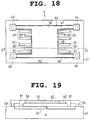
- FIG. 18 shows a plan view of the sensor and in FIG. 19 a cross sectional view taken along line E-E of FIG. 18 is shown.
- a beam structure 63 is disposed on a silicon substrate 41.
- the beam structure 63 made of polysilicon is constructed of anchor sections 43, 44, 45, and 46 and movable section 42, disposed spaced at a prescribed distance above silicon substrate 41.
- movable section 42 comprises beam sections 47 and 48, a weight section 49, and a movable electrode section 50. That is, beam sections 47 and 48 are extended from anchor sections 43, 44, 45, and 46, and weight section 49 is supported in these beam sections 47 and 48.
- the movable electrode section 50 is formed in one portion of this weight section 49.
- a pair of fixed electrodes 51 corresponding to one movable electrode section 50 is disposed so that they are facing one another on silicon substrate 41.
- the above differential capacity-type semiconductor acceleration sensor is considered to be an improved MIS transistor-type semiconductor acceleration sensor.
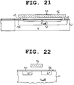
- FIG. 20 shows a plan view of the sensor
- FIG. 21 the cross sectional view taken along line F-F of FIG. 20 is shown
- FIG. 22 the cross sectional view taken along line G-G of FIG. 20 is shown
- FIG. 23 the cross sectional view taken along line H-H of FIG. 20 is shown.
- peripheral circuit 59 and beam structure 63 are electrically connected, and peripheral circuit 59 and fixed electrodes 55 to 58 are electrically connected; moreover, peripheral circuit 59 and underlying electrode 52 are electrically connected. More concretely, the electrical connection of peripheral circuit 59 and beam structure 63 is as shown in FIG. 24: a wiring material 60 such as Al-Si is extended from peripheral circuit 59, and this wiring material 60 and beam structure 63 are connected via impurity diffusion region 61. A voltage generated by this peripheral circuit 59 is applied to beam structure 63.
- a voltage is applied between beam structure 63 and silicon substrate 41, and a voltage is applied between fixed electrodes 55 and 56, and between fixed electrodes 57 and 58.
- an acceleration changes in a parallel direction (shown by Z in FIG. 20) on the surface of silicon substrate 41 and variation in a current (drain current) between fixed electrodes 55 and 56, and between fixed electrodes 57 and 58, occurs due to displacement of movable electrode sections 53 and 54.
- This variation in current is measured by peripheral circuit 59 and applied acceleration is detected.
- peripheral circuit 59 and beam structure 63 are formed by impurity diffusion region 61.
- impurity diffusion region 61 the electrical connection between peripheral circuit 59 and beam structure 63 is formed by impurity diffusion region 61.
- leakage current occurs from impurity diffusion region 61 to the silicon substrate 41 side giving rise to loss of voltage applied to beam structure 63. That is, despite the prescribed voltage being produced by peripheral circuit 59, only the voltage lost by the leakage current is applied to beam structure 63.
- channel 62 is formed between fixed electrodes (source and drain electrodes) 55 to 58 and underlying electrode 52, leakage current occurs and there is also the problem of deterioration of sensor characteristics.
- an object of the present invention is to provide a semiconductor acceleration sensor and manufacturing method thereof capable of reducing leakage current.
- a first aspect of the present invention is that, in a semiconductor acceleration sensor which detects an acceleration from a displacement of a movable section provided with a semiconductor substrate, a beam structure having the movable section disposed spaced at a prescribed distance above the semiconductor substrate, and a peripheral circuit formed in the semiconductor substrate and electrically connected to the beam structure, an electro-conductive thin film for connecting the beam structure to the peripheral circuit is provided.
- the beam structure and the peripheral circuit are connected electrically by the electro-conductive thin film'.
- the beam structure and the peripheral circuit are connected through an impurity diffusion layer formed in the semiconductor substrate, a leakage current occurs from the impurity diffusion layer.
- no impurity diffusion layer for connecting between the beam structure and the peripheral circuit is provided, no leakage current occurs.
- the electro-conductive thin film can be the same material as a gate electrode of a MOS transistor formed in the peripheral circuit.
- the electro-conductive thin film utilizes the same material as a gate electrode of a peripheral circuit MOS transistor, the number of manufacturing processes is not increased in order to form the electro-conductive thin film.
- the electro-conductive thin film in a case where the electro-conductive thin film is disposed on an upper layer side in the connecting portion, the electro-conductive thin film can be an extruded metal wiring film extended from the peripheral circuit.
- the beam structure and the peripheral circuit are electrically connected by only one layer of the wiring film extended from the peripheral circuit, there is only one electrical connection point in the wiring between the wiring film and the beam structure, and therefore the electrical connection point is restricted to the absolute minimum.
- a second aspect of the present invention is a semiconductor acceleration sensor, which detects an applied acceleration from variation in a current between fixed electrodes, comprising a semiconductor substrate, a beam structure having a movable section disposed spaced at a predetermined distance above the semiconductor substrate, a movable electrode section being composed of one portion of the movable section, a pair of fixed electrodes of impurity diffusion layers formed in said semiconductor substrate so as to oppose to both sides of the movable electrode section, an underlying electrode of an impurity diffusion layer formed in a region of the semiconductor substrate where the underlying electrode faces the movable section while at least no fixed electrodes are provided to reduce electrostatic force produced between the movable section and the semiconductor substrate, and further characterized by a leakage current prevention region disposed between the fixed electrodes and the underlying electrode.
- a leakage current prevention region there is a thick oxide film for prevention of channel-formation. Furthermore, the impurity concentration of the semiconductor substrate can be increased locally to thereby make the threshold value high.
- a width of passage through which the leakage current flows may be narrowed to reduce the leakage current.
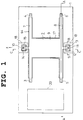
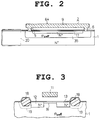
- FIG. 1 shows a plan view of a semiconductor acceleration sensor of the present embodiment. Further, the cross section A-A of FIG. 1 is shown in FIG. 2, the cross section B-B of FIG. 1 is shown in FIG. 3 and the cross section C-C of FIG. 1 is shown in FIG. 4.
- the present embodiment becomes an MIS transistor-type semiconductor acceleration sensor.
- a P well region 35 is formed and a beam structure 64 made from a polysilicon thin film is provided in the top surface of this P well region 35.
- the beam structure 64 is constructed from anchor sections 3, 4, 5 and 6, and a movable section 2 disposed spaced at a predetermined distance above silicon substrate 1.
- movable section 2 comprises beam sections 7 and 8, weight (mass) section 9 and movable electrode sections 10 and 11.
- anchor sections 3, 4, 5 and 6, respectively, are protrudingly disposed on silicon substrate 1.
- a belt-form beam section 7 is extended spaced at a predetermined distance above silicon substrate 1 connecting anchor section 3 and anchor section 4.
- another belt-form beam section 8 is extended spaced at the predetermined distance above silicon substrate 1 connecting anchor section 5 and anchor section 6.
- a weight section 9 is disposed in a central portion in a lengthwise direction of both beam sections 7 and 8 at the predetermined distance above silicon substrate 1.
- a lengthwise-shaped movable electrode section 10 is protrudingly disposed in a central portion in a lengthwise direction of beam section 7.
- another lengthwise-shaped movable electrode section 11 is protrudingly disposed in a central portion in a lengthwise direction of beam section 8.
- fixed electrodes 12 and 13 (made of an impurity diffusion layer) are formed in the surface of silicon substrate 1 so as to correspond to either side of the movable electrode section 11.
- Fixed electrodes 12 and 13 are formed by the introduction of N+ impurities into silicon substrate 1 by a method such as ion implantation.
- another pair of fixed electrodes 14 and 15, each being of an impurity diffusion layer is formed in the surface of silicon substrate 1 to correspond to the other movable electrode section 10.
- an inversion layer 16 is formed between electrodes 12 and 13 in silicon substrate 1, this inversion layer 16 develops as a result of a voltage being applied between silicon substrate 1 and movable electrode section 11.
- an inversion layer (not shown) is formed between electrodes 14 and 15 in silicon substrate 1, this inversion layer develops as a result of a voltage being applied between silicon substrate 1 and movable electrode section 10.
- underlying electrode 17 is formed by means of an N+ impurity diffusion layer in a portion facing movable section 2 in silicon substrate 1 at least not containing fixed electrodes 12, 13, 14 and 15.
- the underlying electrode is to reduce electrostatic force occurring between silicon substrate 1 and movable electrode section 2 by having the same electric potential as movable section 2 (movable sections 10, 11).
- LOCOS film silicon oxide films 18 formed by means of a LOCOS method (hereinafter referred to LOCOS film) are provided, and below the respective LOCOS films 18 a channel stopper layer 19 is provided.
- Channel stopper layer 19 is formed by the implantation of a B (Boron) ion.
- a leakage current prevention member is constructed from this LOCOS film 18 and channel stopper layer 19.
- peripheral circuit 20 is formed in silicon substrate 1; this peripheral circuit 20 and beam structure 64 are electrically connected, and peripheral circuit 20 and fixed electrodes 12, 13, 14 and 15 are electrically connected and furthermore peripheral circuit 20 and underlying electrode 17 are electrically connected.
- a MOS transistor is formed within a peripheral circuit 20. That is, an N well region 21 is formed within silicon substrate 1, a P+ source region 22 and a P+ drain region 23 are formed in the N well region 21 and a polysilicon gate electrode 25 is formed on a silicon oxide film 24 as a gate oxide film. Meanwhile, a silicon oxide film 26 is formed on the surface of silicon substrate 1 in a beam structure forming region. On top of that, an electro-conductive thin film 27 made of polysilicon is formed. On top of the electro-conductive thin film 27, the anchor section 5 of the beam structure 64 is disposed. Electro-conductive thin film 27 is also formed on LOCOS film 28 on silicon substrate 1. The end section of the electro-conductive thin film 27 is connected to a drain region 23 of the MOS transistor via an Al-Si film 29.
- This construction is formed in the following way. First, source region 22 and drain region 23 of MOS transistor are formed in the surface of silicon substrate 1, utilizing well known semiconductor manufacturing technology. After that, a polysilicon thin film becoming a polysilicon gate electrode 25 is deposited, it is processed into the desired pattern and polysilicon gate electrode 25 is formed. At this time, polysilicon thin film also remains at the wiring points of beam structure 64 and peripheral circuit 20 and forms electro-conductive thin film 27. Next, BPSG film 30 is deposited by a CVD method, the BPSG film 30 of the point connecting beam structure 64 is opened, a polysilicon film making beam structure 64 is deposited at around 600 °C and it is processed into the desired pattern.
- the BPSG film 30 of the point connecting the Al-Si film 29 is opened, Al-Si film 29 is deposited by a spattering process and it is processed into the desired pattern. After this, the BPSG film 30 under movable section 2 is removed by etching and a condition of displacement is made possible. Finally, annealing is performed and ohmic contact is ensured.
- peripheral circuit 20 not only a MOS transistor, but a Bi-CMOS may also be built up.
- a predetermined voltage is produced by peripheral circuit 20 and the predetermined voltage is applied to beam structure 64 passing through Al-Si film 29 and electro-conductive thin film 27 in FIG. 5.
- an electro-conductive thin film 27 made of polysilicon as a wiring material, a leakage current to the substrate 1 is prevented.
- Al-Si film 29 is connected to electro-conductive thin film 27 from above of the electro-conductive thin film 27. Therefore, by the electroconductive thin film 27 being disposed thus, wiring contact defects are of the same level as in peripheral circuit 20; namely, they do not occur.
- a voltage is applied by the peripheral circuit 20 between beam structure 64 (movable electrode sections 10 and 11) and silicon substrate 1, a voltage is applied between fixed electrodes 12 and 13 and between fixed electrodes 14 and 15; inversion layer 16 is formed; and a current flows between fixed electrodes 12 and 13 and also between fixed electrodes 14 and 15.
- this acceleration sensor receives an acceleration and movable section 2 displaces in direction X shown in FIG. 1 (a parallel direction in the surface of substrate 1), the width of the inversion layer formation region (called the 'gate width' in a transistor) between fixed electrodes 12 and 13, and also between fixed electrodes 14 and 15 changes. The result is that the current flowing in fixed electrodes 12 and 13 is reduced and, to the contrary, the current flowing between fixed electrodes 14 and 15 increases.
- the peripheral circuit 20 detects an acceleration by measuring these currents between the fixed electrodes.
- peripheral circuit 20 reduces electrostatic force occurring between silicon substrate 1 and movable section 2 by making the electrical potential of the underlying electrode 17 the same as the electrical potential of beam structure 64 (movable electrode sections 10 and 11).
- electro-conductive thin film 27 is of polysilicon, the same as gate electrode 25 of the MOS transistor formed in the peripheral circuit, electro-conductive thin film 27 can be formed at the same time as the forming of gate electrode 25, and it is unnecessary to increase the number of manufacturing processes in order to form electro-conductive thin film 27.
- a leakage current prevention member made of LOCOS film 18 and channel stopper layer 19 is disposed between fixed electrodes 12 - 15 in silicon substrate 1 and underlying electrode 17. Further, even when a voltage is applied to movable section 2 which makes a gate section, the occurrence of leakage current between fixed electrodes (source, drain electrodes) 12-15 and underlying electrode 17 can be controlled, and stable sensor characteristics can be obtained.
- electro-conductive thin film 27 can be utilized other gate electrode material such as aluminum or platinum, or a thin metal film such as an aluminum group metal, titanium, tungsten, chromium, silicon, zirconium, platinum or nickel.
- gate electrode material such as aluminum or platinum
- a thin metal film such as an aluminum group metal, titanium, tungsten, chromium, silicon, zirconium, platinum or nickel.
- a second embodiment will be described hereinafter mainly on the differences between it and the first embodiment.
- FIG. 6 corresponds to FIG. 5 in the first embodiment, showing the construction of an electrical connection between peripheral circuit 20 and beam structure 64.
- a MOS transistor is formed in a peripheral circuit 20. That is, an N well region 21 is formed in a silicon substrate 1, a P+ source region 22 and a P+ drain region 23 are formed in N well region 21, and a polysilicon gate electrode 25 is formed on a silicon oxide film 24 as a gate oxide film. Meanwhile, anchor section 5 of beam structure 64 is formed in a beam structure forming region. This beam structure 64 is made of a polysilicon film, and a thin film thickness portion 2b which is served as a connection portion is extended from a main body portion 2a of movable section 2.
- a thin portion 2b with a film thickness t2 (e.g., 0.7 ⁇ m), thinner than the film thickness of main body portion 2a (e.g., 2 ⁇ m), is provided.
- the end of thin portion 2b of movable section 2 is disposed on top of a BPSG film 30.
- an Al-Si film 29 extended from drain region 23 of MOS transistor of the peripheral circuit 20 is disposed, and peripheral circuit 20 and beam structure 64 are electrically connected only by this Al-Si film 29.
- This construction is formed in the following way.
- a MOS transistor source region 22 and drain region 23 are formed in the surface of silicon substrate 1, utilizing well known semiconductor manufacturing technology.
- a silicon oxide film 24 is formed, then a polysilicon thin film is deposited and, processed into the desired pattern, forms polysilicon gate electrode 25.
- BPSG film 30 is deposited by a CVD method or a spattering method, and a window 36 is formed by etching in BPSG film 30 at a point facing the anchor section 5 of beam structure 64.
- polysilicon film 37 which becomes beam structure 64 is deposited by an LPCVD method at around 600 °C. At this time, the film thickness of polysilicon film 37 becomes t1 (e.g., 2 ⁇ m).
- polysilicon film 37 is etched down to a predetermined thickness t2 (e.g., 0.7 ⁇ m).
- t2 e.g., 0.7 ⁇ m
- anisotropic etching by KOH or isotropic etching by fluoric and nitric (HF-HN03-H202) acids is utilized.
- the deposited polysilicon film 37 of the other regions is stripped by isotropic etching.
- movable section 2 having main body portion 2a and thin portion for connection 2b, is patterned.
- BPSG film 30 above the MOS transistor drain region 23 is etched and contact hole 40 is formed.
- Al-Si film 29 is deposited by spattering. At this time, Al-Si film 29 is also disposed above the movable section 2 including thin portion 2b. Because the film thickness of movable section 2 is made thin at portion 2b, there is no occurrence of step cutting of the Al-Si film 29.
- the Al-Si film 29 is processed into the desired pattern. Furthermore, as shown in FIG. 6, the BPSG film 30 below movable section 2 is etched utilizing HF based etching liquid, and movable section 2 is in a condition capable of displacement. At this time, at least the BPSG film 30 below Al-Si film 29 is retained. Finally, annealing which is so-called aluminum sintering is performed, and ohmic contact is ensured.
- beam structure 64 and peripheral circuit 20 are electrically connected by an Al-Si film 29 (wiring film) of one layer extended from peripheral circuit 20. That is, beam structure 64 and peripheral circuit 20 are electrically connected by an Al-Si film 29 formed by a one time film.
- the electrical connection points are two points: i.e., between beam structure 64 and impurity diffusion region 61, and between impurity diffusion region 61 and wiring material 60. Further, in FIG.
- the electrical connection points are two points: i.e., between beam structure 64 and electro-conductive thin film 27, and between electro-conductive thin film 27 and Al-Si film 29.
- a portion for connection 2b with a thin thickness in comparison with the other portions is provided in one portion of beam structure 64 and disposed on BPSG film 30 (insulation film) to connect beam structure 64 with Al-Si film 29 (wiring film) extended from peripheral circuit 20. Therefore, in the case where Al-Si film 29 is disposed on the beam structure 64; because the connection point of beam structure 64 to Al-Si film 29 is thinned, the step becomes small and cutting of Al-Si film 29 does not occur. On the other hand, when the connection point of beam structure 64 to Al-Si film 29 is not thinned, the step is large and step coverage is bad, thereby causing the occurrence of cutting in the Al-Si film 29.
- a BPSG film 30 (insulation film) is formed on a silicon substrate 1 (semiconductor substrate) and a polysilicon film 37 (beam structure forming film) is formed on top of this BPSG film 30 (First Process); polysilicon film 37 is etched to a prescribed thickness in a condition with beam structure 64 forming portion in polysilicon film 37 (excepting the portion making junction 2b) being masked (Second Process); polysilicon film 37 is stripped by etching with beam structure 64 forming portion in polysilicon film 37 masked (Third Process); an Al-Si film 29 (thin film wiring material) electrically connecting a point in polysilicon film 37 making junction 2b and a peripheral circuit 20 is formed (Fourth Process); BPSG film 30 under polysilicon film 37 (except for at least the points of disposing Al-Si film 29) is removed by etching and beam structure 64 is formed
- a thin film wiring material a pure aluminum film or an aluminum alloy film etc. are used.
- this aluminum alloy film there are such as Al-Cu film, Al-Si-Cu film and Al-Si film.
- a Bi-CMOS or bipolar transistor may also be built up.
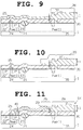
- FIGS. 12 and 13 show a plan view of the sensor
- FIG. 13 shows cross section D-D in FIG. 12.
- trench 31 is formed so as to surround a pair of fixed electrodes 12 and 13 and filled with an insulation film 32 such as a silicon oxide. By doing so in this way, the occurrence of leakage current is prevented.
- cutting portions 33 are formed from both sides facing movable electrode section 11 between fixed electrodes 12 and 13 and underlying electrode 17, and that width becomes narrow. By doing so in this way, as shown in FIG. 15, compared to a case where there are no cutting portions, the leakage current passage becomes narrow and leakage current can be reduced. That is to say, the channel width of the transistor parasitically formed between underlying electrode 17 and fixed electrodes 12 and 13 becomes narrow and leakage current is reduced.
- this actual width can be made narrow by a penetrating hole 34 being formed in movable electrode section 11 which is between fixed electrodes 12 and 13 and underlying electrode 17.
- the impurity concentration of the substrate higher locally as a channel stopper corresponding to the channel formation region of the parasitic transistor, a leakage current reduction effect can be obtained.
- an embodiment in the following fashion may be also possible.
- a beam structure 63 and a peripheral circuit in a differential capacity-type semiconductor acceleration sensor shown in FIG. 18 are electrically connected by means of an electro-conductive thin film 27 shown in FIG. 5, or are electrically connected by a single-layer wiring film 29 shown in FIG. 6.
Landscapes
- Physics & Mathematics (AREA)
- General Physics & Mathematics (AREA)
- Pressure Sensors (AREA)
Applications Claiming Priority (6)
| Application Number | Priority Date | Filing Date | Title |
|---|---|---|---|
| JP3614094 | 1994-03-07 | ||
| JP3614094 | 1994-03-07 | ||
| JP36140/94 | 1994-03-07 | ||
| JP244397/94 | 1994-10-07 | ||
| JP24439794A JP3435844B2 (ja) | 1994-03-07 | 1994-10-07 | 半導体加速度センサ及びその製造方法 |
| JP24439794 | 1994-10-07 |
Publications (3)
| Publication Number | Publication Date |
|---|---|
| EP0671629A2 true EP0671629A2 (de) | 1995-09-13 |
| EP0671629A3 EP0671629A3 (de) | 1999-06-16 |
| EP0671629B1 EP0671629B1 (de) | 2003-05-14 |
Family
ID=26375187
Family Applications (1)
| Application Number | Title | Priority Date | Filing Date |
|---|---|---|---|
| EP95103255A Expired - Lifetime EP0671629B1 (de) | 1994-03-07 | 1995-03-07 | Beschleunigungssensor und Verfahren zu seiner Herstellung |
Country Status (4)
| Country | Link |
|---|---|
| US (1) | US5619050A (de) |
| EP (1) | EP0671629B1 (de) |
| JP (1) | JP3435844B2 (de) |
| DE (1) | DE69530716T2 (de) |
Cited By (7)
| Publication number | Priority date | Publication date | Assignee | Title |
|---|---|---|---|---|
| EP0816856A1 (de) * | 1996-07-03 | 1998-01-07 | Murata Manufacturing Co., Ltd. | Elektrostatischer kapazitiver Sensor und Verfahren zu seiner Herstellung |
| US5808331A (en) * | 1995-09-05 | 1998-09-15 | Motorola, Inc. | Monolithic semiconductor device having a microstructure and a transistor |
| US5818093A (en) * | 1996-01-25 | 1998-10-06 | Motorola, Inc. | Semiconductor device having a movable gate |
| US5903038A (en) * | 1997-06-30 | 1999-05-11 | Motorola, Inc. | Semiconductor sensing device and method for fabricating the same |
| US5929472A (en) * | 1997-04-07 | 1999-07-27 | Motorola, Inc. | Semiconductor floating gate sensor device |
| EP0836265A4 (de) * | 1996-04-26 | 2000-09-13 | Nippon Signal Co Ltd | Elektromagnetischer betätiger und verfahren zu seiner herstellung |
| CN101891140B (zh) * | 2006-10-24 | 2012-12-12 | 精工爱普生株式会社 | Mems器件 |
Families Citing this family (17)
| Publication number | Priority date | Publication date | Assignee | Title |
|---|---|---|---|---|
| JP3435850B2 (ja) * | 1994-10-28 | 2003-08-11 | 株式会社デンソー | 半導体力学量センサ及びその製造方法 |
| US5578224A (en) * | 1995-06-07 | 1996-11-26 | Analog Devices, Inc. | Method of making micromachined device with ground plane under sensor |
| US5922212A (en) * | 1995-06-08 | 1999-07-13 | Nippondenso Co., Ltd | Semiconductor sensor having suspended thin-film structure and method for fabricating thin-film structure body |
| US6448624B1 (en) * | 1996-08-09 | 2002-09-10 | Denso Corporation | Semiconductor acceleration sensor |
| US6220096B1 (en) * | 1997-03-20 | 2001-04-24 | Interscience, Inc. | Differential wideband vibration |
| JP3555388B2 (ja) * | 1997-06-30 | 2004-08-18 | 株式会社デンソー | 半導体ヨーレートセンサ |
| JPH1194863A (ja) * | 1997-09-12 | 1999-04-09 | Nikon Corp | カンチレバー及びその製造方法 |
| US6720634B2 (en) * | 2002-01-07 | 2004-04-13 | Honeywell International Inc. | Contactless acceleration switch |
| CN100371718C (zh) * | 2003-07-10 | 2008-02-27 | 友达光电股份有限公司 | 电容式加速传感器 |
| JP2009145321A (ja) * | 2007-11-19 | 2009-07-02 | Hitachi Ltd | 慣性センサ |
| JP5417737B2 (ja) * | 2008-04-23 | 2014-02-19 | パナソニック株式会社 | 慣性力センサ |
| JP2011047732A (ja) * | 2009-08-26 | 2011-03-10 | Seiko Epson Corp | Memsセンサー、memsセンサーの製造方法および電子機器 |
| JP2011075543A (ja) * | 2009-09-07 | 2011-04-14 | Seiko Epson Corp | 物理量センサー、物理量センサーの製造方法、および電子機器 |
| JP2011128132A (ja) * | 2009-11-19 | 2011-06-30 | Seiko Epson Corp | 物理量センサー、物理量センサーの製造方法、および電子機器 |
| CN102510998A (zh) * | 2009-11-25 | 2012-06-20 | 阿尔卑斯电气株式会社 | 测力传感器 |
| DE102010012607B4 (de) * | 2010-03-24 | 2012-01-26 | Eads Deutschland Gmbh | HF-MEMS-Schalter |
| US20120146452A1 (en) * | 2010-12-10 | 2012-06-14 | Miradia, Inc. | Microelectromechanical system device and semi-manufacture and manufacturing method thereof |
Family Cites Families (15)
| Publication number | Priority date | Publication date | Assignee | Title |
|---|---|---|---|---|
| JPS6055655A (ja) * | 1983-09-07 | 1985-03-30 | Nissan Motor Co Ltd | 梁構造体を有する半導体装置 |
| FR2578323B1 (fr) * | 1985-03-01 | 1987-11-20 | Metravib Sa | Capteur integre de grandeurs mecaniques a effet capacitif et procede de fabrication. |
| JPS61212052A (ja) * | 1985-03-18 | 1986-09-20 | Nissan Motor Co Ltd | 梁構造体を有する半導体装置 |
| US4674319A (en) * | 1985-03-20 | 1987-06-23 | The Regents Of The University Of California | Integrated circuit sensor |
| US5343064A (en) * | 1988-03-18 | 1994-08-30 | Spangler Leland J | Fully integrated single-crystal silicon-on-insulator process, sensors and circuits |
| DE3814952A1 (de) * | 1988-05-03 | 1989-11-23 | Bosch Gmbh Robert | Sensor |
| US5101669A (en) * | 1988-07-14 | 1992-04-07 | University Of Hawaii | Multidimensional force sensor |
| US4930043A (en) * | 1989-02-28 | 1990-05-29 | United Technologies | Closed-loop capacitive accelerometer with spring constraint |
| US5126812A (en) * | 1990-02-14 | 1992-06-30 | The Charles Stark Draper Laboratory, Inc. | Monolithic micromechanical accelerometer |
| JPH0425764A (ja) * | 1990-05-21 | 1992-01-29 | Nec Corp | 半導体加速度センサ |
| US5326726A (en) * | 1990-08-17 | 1994-07-05 | Analog Devices, Inc. | Method for fabricating monolithic chip containing integrated circuitry and suspended microstructure |
| EP0543901B1 (de) * | 1990-08-17 | 1995-10-04 | Analog Devices, Inc. | Monolithischer beschleunigungsmesser |
| US5075641A (en) * | 1990-12-04 | 1991-12-24 | Iowa State University Research Foundation, Inc. | High frequency oscillator comprising cointegrated thin film resonator and active device |
| FR2687778B1 (fr) * | 1992-02-20 | 1994-05-20 | Sextant Avionique | Micro-capteur capacitif a capacite parasite reduite et procede de fabrication. |
| EP0646246B1 (de) * | 1992-06-17 | 1997-03-26 | Analog Devices, Inc. | Verfahren zur herstellung eines eine integrierte halbleiterschaltung und eine selbsttragende mikrostruktur enthaltenden monolithischen chip |
-
1994
- 1994-10-07 JP JP24439794A patent/JP3435844B2/ja not_active Expired - Fee Related
-
1995
- 1995-03-06 US US08/399,345 patent/US5619050A/en not_active Expired - Lifetime
- 1995-03-07 EP EP95103255A patent/EP0671629B1/de not_active Expired - Lifetime
- 1995-03-07 DE DE69530716T patent/DE69530716T2/de not_active Expired - Lifetime
Cited By (10)
| Publication number | Priority date | Publication date | Assignee | Title |
|---|---|---|---|---|
| US5808331A (en) * | 1995-09-05 | 1998-09-15 | Motorola, Inc. | Monolithic semiconductor device having a microstructure and a transistor |
| US5818093A (en) * | 1996-01-25 | 1998-10-06 | Motorola, Inc. | Semiconductor device having a movable gate |
| EP0836265A4 (de) * | 1996-04-26 | 2000-09-13 | Nippon Signal Co Ltd | Elektromagnetischer betätiger und verfahren zu seiner herstellung |
| EP0816856A1 (de) * | 1996-07-03 | 1998-01-07 | Murata Manufacturing Co., Ltd. | Elektrostatischer kapazitiver Sensor und Verfahren zu seiner Herstellung |
| US6051855A (en) * | 1996-07-03 | 2000-04-18 | Murata Manufacturing Co., Ltd. | Electrostatic capacitive sensor |
| US6265238B1 (en) | 1996-07-03 | 2001-07-24 | Murata Manufacturing Co., Ltd. | Electrostatic capacitive sensor and method for manufacturing the same |
| US5929472A (en) * | 1997-04-07 | 1999-07-27 | Motorola, Inc. | Semiconductor floating gate sensor device |
| US5903038A (en) * | 1997-06-30 | 1999-05-11 | Motorola, Inc. | Semiconductor sensing device and method for fabricating the same |
| CN101891140B (zh) * | 2006-10-24 | 2012-12-12 | 精工爱普生株式会社 | Mems器件 |
| CN102173374B (zh) * | 2006-10-24 | 2013-01-02 | 精工爱普生株式会社 | Mems 器件 |
Also Published As
| Publication number | Publication date |
|---|---|
| DE69530716T2 (de) | 2004-03-18 |
| EP0671629A3 (de) | 1999-06-16 |
| JP3435844B2 (ja) | 2003-08-11 |
| JPH07301640A (ja) | 1995-11-14 |
| US5619050A (en) | 1997-04-08 |
| DE69530716D1 (de) | 2003-06-18 |
| EP0671629B1 (de) | 2003-05-14 |
Similar Documents
| Publication | Publication Date | Title |
|---|---|---|
| EP0671629B1 (de) | Beschleunigungssensor und Verfahren zu seiner Herstellung | |
| JP4003326B2 (ja) | 半導体力学量センサおよびその製造方法 | |
| US5414284A (en) | ESD Protection of ISFET sensors | |
| US6137150A (en) | Semiconductor physical-quantity sensor having a locos oxide film, for sensing a physical quantity such as acceleration, yaw rate, or the like | |
| US5514898A (en) | Semiconductor device with a piezoresistive pressure sensor | |
| EP0762510A2 (de) | Verfahren zum Herstellen einer monolithischen Halbleiteranordnung mit integrierten mikrogefertigten Oberflächestrukturen | |
| US20110108932A1 (en) | Micromechanical Capacitive Sensor Element | |
| US5503017A (en) | Semiconductor acceleration sensor | |
| US4547789A (en) | High current thin film transistor | |
| JP4665942B2 (ja) | 半導体力学量センサ | |
| EP0215493B1 (de) | Geschützte MOS-Transistorschaltung | |
| JP3551527B2 (ja) | 半導体感歪センサの製造方法 | |
| US5869876A (en) | Semiconductor strain sensor | |
| US5534454A (en) | Method of producing a semiconductor device having accurate current detection | |
| EP1164640B1 (de) | Halbleiterbauelement und dessen herstelllung | |
| JPH08293543A (ja) | 半導体装置及びその製造方法 | |
| US5932921A (en) | Sensor chip having a diode portions and a thin-wall portion | |
| JPS6317560A (ja) | Mos型半導体装置 | |
| US20070254387A1 (en) | Semiconductor strain gauge and the manufacturing method | |
| US6281553B1 (en) | Semiconductor device, electrostatic discharge protection device, and dielectric breakdown preventing method | |
| JP3331648B2 (ja) | 半導体加速度センサ | |
| JP3633555B2 (ja) | 半導体力学量センサ | |
| JP4479344B2 (ja) | Soi基板のゲート酸化膜の評価方法 | |
| JP3477924B2 (ja) | 半導体力学量センサの製造方法 | |
| JP3326905B2 (ja) | 半導体加速度センサ |
Legal Events
| Date | Code | Title | Description |
|---|---|---|---|
| PUAI | Public reference made under article 153(3) epc to a published international application that has entered the european phase |
Free format text: ORIGINAL CODE: 0009012 |
|
| AK | Designated contracting states |
Kind code of ref document: A2 Designated state(s): DE FR GB |
|
| RAP1 | Party data changed (applicant data changed or rights of an application transferred) |
Owner name: DENSO CORPORATION |
|
| PUAL | Search report despatched |
Free format text: ORIGINAL CODE: 0009013 |
|
| AK | Designated contracting states |
Kind code of ref document: A3 Designated state(s): DE FR GB |
|
| 17P | Request for examination filed |
Effective date: 19990423 |
|
| 17Q | First examination report despatched |
Effective date: 20010418 |
|
| GRAH | Despatch of communication of intention to grant a patent |
Free format text: ORIGINAL CODE: EPIDOS IGRA |
|
| GRAH | Despatch of communication of intention to grant a patent |
Free format text: ORIGINAL CODE: EPIDOS IGRA |
|
| GRAA | (expected) grant |
Free format text: ORIGINAL CODE: 0009210 |
|
| AK | Designated contracting states |
Designated state(s): DE FR GB |
|
| REG | Reference to a national code |
Ref country code: GB Ref legal event code: FG4D |
|
| REF | Corresponds to: |
Ref document number: 69530716 Country of ref document: DE Date of ref document: 20030618 Kind code of ref document: P |
|
| ET | Fr: translation filed | ||
| PLBE | No opposition filed within time limit |
Free format text: ORIGINAL CODE: 0009261 |
|
| STAA | Information on the status of an ep patent application or granted ep patent |
Free format text: STATUS: NO OPPOSITION FILED WITHIN TIME LIMIT |
|
| 26N | No opposition filed |
Effective date: 20040217 |
|
| PGFP | Annual fee paid to national office [announced via postgrant information from national office to epo] |
Ref country code: GB Payment date: 20130306 Year of fee payment: 19 Ref country code: DE Payment date: 20130227 Year of fee payment: 19 Ref country code: FR Payment date: 20130325 Year of fee payment: 19 |
|
| REG | Reference to a national code |
Ref country code: DE Ref legal event code: R119 Ref document number: 69530716 Country of ref document: DE |
|
| GBPC | Gb: european patent ceased through non-payment of renewal fee |
Effective date: 20140307 |
|
| REG | Reference to a national code |
Ref country code: FR Ref legal event code: ST Effective date: 20141128 |
|
| REG | Reference to a national code |
Ref country code: DE Ref legal event code: R119 Ref document number: 69530716 Country of ref document: DE Effective date: 20141001 |
|
| PG25 | Lapsed in a contracting state [announced via postgrant information from national office to epo] |
Ref country code: FR Free format text: LAPSE BECAUSE OF NON-PAYMENT OF DUE FEES Effective date: 20140331 Ref country code: GB Free format text: LAPSE BECAUSE OF NON-PAYMENT OF DUE FEES Effective date: 20140307 Ref country code: DE Free format text: LAPSE BECAUSE OF NON-PAYMENT OF DUE FEES Effective date: 20141001 |