EP0672899B1 - Halbleiter-Druckwandler mit Einkristall-Silizium-Membran und Einkristall-Dehnungsmessstreifen und Herstellungsverfahren dazu - Google Patents
Halbleiter-Druckwandler mit Einkristall-Silizium-Membran und Einkristall-Dehnungsmessstreifen und Herstellungsverfahren dazu Download PDFInfo
- Publication number
- EP0672899B1 EP0672899B1 EP95103971A EP95103971A EP0672899B1 EP 0672899 B1 EP0672899 B1 EP 0672899B1 EP 95103971 A EP95103971 A EP 95103971A EP 95103971 A EP95103971 A EP 95103971A EP 0672899 B1 EP0672899 B1 EP 0672899B1
- Authority
- EP
- European Patent Office
- Prior art keywords
- silicon
- forming
- crystal
- diaphragm
- sensor
- Prior art date
- Legal status (The legal status is an assumption and is not a legal conclusion. Google has not performed a legal analysis and makes no representation as to the accuracy of the status listed.)
- Expired - Lifetime
Links
Images


Classifications
-
- G—PHYSICS
- G01—MEASURING; TESTING
- G01L—MEASURING FORCE, STRESS, TORQUE, WORK, MECHANICAL POWER, MECHANICAL EFFICIENCY, OR FLUID PRESSURE
- G01L9/00—Measuring steady of quasi-steady pressure of fluid or fluent solid material by electric or magnetic pressure-sensitive elements; Transmitting or indicating the displacement of mechanical pressure-sensitive elements, used to measure the steady or quasi-steady pressure of a fluid or fluent solid material, by electric or magnetic means
- G01L9/0041—Transmitting or indicating the displacement of flexible diaphragms
- G01L9/0051—Transmitting or indicating the displacement of flexible diaphragms using variations in ohmic resistance
- G01L9/0052—Transmitting or indicating the displacement of flexible diaphragms using variations in ohmic resistance of piezoresistive elements
- G01L9/0055—Transmitting or indicating the displacement of flexible diaphragms using variations in ohmic resistance of piezoresistive elements bonded on a diaphragm
-
- G—PHYSICS
- G01—MEASURING; TESTING
- G01L—MEASURING FORCE, STRESS, TORQUE, WORK, MECHANICAL POWER, MECHANICAL EFFICIENCY, OR FLUID PRESSURE
- G01L9/00—Measuring steady of quasi-steady pressure of fluid or fluent solid material by electric or magnetic pressure-sensitive elements; Transmitting or indicating the displacement of mechanical pressure-sensitive elements, used to measure the steady or quasi-steady pressure of a fluid or fluent solid material, by electric or magnetic means
- G01L9/0041—Transmitting or indicating the displacement of flexible diaphragms
- G01L9/0042—Constructional details associated with semiconductive diaphragm sensors, e.g. etching, or constructional details of non-semiconductive diaphragms
-
- Y—GENERAL TAGGING OF NEW TECHNOLOGICAL DEVELOPMENTS; GENERAL TAGGING OF CROSS-SECTIONAL TECHNOLOGIES SPANNING OVER SEVERAL SECTIONS OF THE IPC; TECHNICAL SUBJECTS COVERED BY FORMER USPC CROSS-REFERENCE ART COLLECTIONS [XRACs] AND DIGESTS
- Y10—TECHNICAL SUBJECTS COVERED BY FORMER USPC
- Y10S—TECHNICAL SUBJECTS COVERED BY FORMER USPC CROSS-REFERENCE ART COLLECTIONS [XRACs] AND DIGESTS
- Y10S148/00—Metal treatment
- Y10S148/136—Resistors
-
- Y—GENERAL TAGGING OF NEW TECHNOLOGICAL DEVELOPMENTS; GENERAL TAGGING OF CROSS-SECTIONAL TECHNOLOGIES SPANNING OVER SEVERAL SECTIONS OF THE IPC; TECHNICAL SUBJECTS COVERED BY FORMER USPC CROSS-REFERENCE ART COLLECTIONS [XRACs] AND DIGESTS
- Y10—TECHNICAL SUBJECTS COVERED BY FORMER USPC
- Y10S—TECHNICAL SUBJECTS COVERED BY FORMER USPC CROSS-REFERENCE ART COLLECTIONS [XRACs] AND DIGESTS
- Y10S438/00—Semiconductor device manufacturing: process
- Y10S438/97—Specified etch stop material
Definitions
- This invention relates to a method for manufacturing semiconductor pressure sensors.
- semiconductor pressure sensors contain a diaphragm of one or more silicon layers for deflecting in response to opposing pressure environments, and piezoresistive elements that are configured for sensing the direction and/or magnitude of diaphragm deflection.
- Dielectric isolation is one technique which increases stability.
- the dielectric ideally isolates semiconductor piezoresistive elements from the diaphragm, the support structure, and other piezoresistive elements.
- Silicon dioxide, SiO2 exemplifies a known dielectric that maintains a nearly constant resistance over significant temperature changes.
- the type of silicon used in the pressure sensor is also important.
- Single-crystal silicon and polycrystalline silicon materials have different properties that influence mechanical strength, sensitivity, and even manufacturability.
- US-A-5,094,401 discloses the fabrication of diaphragm pressure sensors utilizing silicon-on-insulator technology.
- an object of this invention is to provide improved semiconductor pressure sensors and associated manufacturing methods, and in particular, for uses which require high temperature stability and high sensitivity.
- Another object of the invention is to provide a high sensitivity semiconductor pressure sensor which is easier to manufacture than competitive existing sensors.
- a further object of this invention is to provide a semiconductor pressure sensor, and a related method of manufacture, for dielectrically isolating single crystal silicon sensors, and further for creating a controllable etch stop configuration for forming the diaphragm.
- the invention features a method for manufacturing semiconductor pressure sensors.
- a silicon-on-insulator (SOI) wafer is provided to include a substrate, a silicon oxide implantation which functions as an etch stop, and surface annealed silicon.
- Epitaxial silicon is grown on the surface silicon to form a single-crystal silicon diaphragm with opposed first and second surfaces.
- the diaphragm is afterwards implanted by a second silicon oxide layer to form a dielectric isolator.
- the second silicon oxide layer is annealed to provide surface silicon for a piezoresistive gage element made of p-type implants.
- the piezoresistive gage element is formed within the surface annealed silicon by boron implantation and by etching to create a dielectrically isolated piezoresistive sensing element. It is preferably provided with additional dielectric isolation by nitride deposition. Evaporated metal, e.g., aluminum, is deposited and etched to provide an external electrical connection to the piezoresistive gage element. The substrate, as part of the SOI wafer, is then etched to provide a backside pressure port such that the diaphragm can deflect in response to a pressure difference between the first and second surfaces.
- Evaporated metal e.g., aluminum
- the silicon oxide implantation which forms the etch stop is confined to a localized and buried volume within the silicon substrate, to form both an etch stop and an over-range cavity support region.
- Oxygen ion implantation is implanted locally by masking portions of the silicon substrate.
- the substrate silicon is epitaxially grown to form a single-crystal silicon diaphragm and piezoresistive gage element, as above.
- the dielectric isolation of the silicon oxide layer provides the sensor with high operating stability and high temperature capability, and also provides an etch stop for backside etching of the pressure port.
- the sensor provides relatively high sensitivity and low pressure differentials, and is relatively easy to manufacture. This enables the device to be coupled more effectively with digital electronics, with the potential for solving other high-performance, intelligent pressure transmitter needs.
- the cavity formed by localized oxygen implantation and etching provides an over-range stop for the diaphragm, resulting in high robustness.
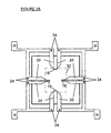
- FIGURES 1 and 1A show a semiconductor pressure sensor 10 constructed in accordance with the invention
- FIGURES 2-2F illustrate the manufacturing stages to fabricate the sensor 10 beginning with a common silicon-on insulator (SOI) wafer.
- SOI silicon-on insulator
- the senor 10 has a single-crystal diaphragm 14 made of epitaxially grown single-crystal silicon disposed between single-crystal p-type gage elements 18 and a silicon substrate 12.
- the substrate 12 includes a localized region of oxygen ion implantation to form a silicon oxide layer 16, which functions as a dielectric isolator and as an etch stop for when the substrate 12 is etched to form the pressure port 32.
- the single-crystal silicon diaphragm 14 is disposed between the oxide layer 16 and another oxide layer 17.
- Layer 17 serves as a dielectric isolator to isolate one gage element 18 from other gage elements 18, and from the diaphragm 14 and the substrate 12.
- the sensor 10 is annealed and implanted with boron ions, in selected localized regions, and selectively etched, to form the gage elements 18 as p-type gage piezoresistors and p+ interconnections 20.
- a nitride deposition layer 22 preferably passivates the p-type piezoresistors 18.
- Metal contacts 24 provide electrical communication to the p+ interconnections 20 and provide a way to externally connect the sensor 10 to a further electrical device.
- the electrical signals produced at the metal contacts 24 are an indication of the pressure differential across the diaphragm 14, i.e., between pressure environments 28 and 30. More particularly, the electrical signals at the contacts 24 are produced by the p-type gage elements 18 and are indicative of a resistance change functionally dependent upon the stress of the diaphragm 14.
- the etched portion 31 of the substrate 12 defines a pyramidal pressure port 32, which exposes the diaphragm 14 to the pressure environment 28, and the substrate 12 supports the sensor 10 at a header interface, e.g., at the mounting headers 26.
- FIGURE 1 showing of the pressure sensor 10, and the similar drawings in FIGURES 2-3, contain exaggerated proportions for clarity of illustration.
- the silicon oxide layer 16, FIGURE 1 is typically 0.45 micron thick
- the etched piezoresistive gage elements 18 are typically 0.4 micron thick.
- FIGURE 1A is a diagrammatic top view (not to scale) of the sensor 10 of FIGURE 1, showing the p+ interconnections 20 and the p-type piezoresistive elements 18.
- the gage elements 18, which preferably inter-connect and form a conventional Wheatstone bridge configuration at the inner ends of the p+ interconnections 20, are located over the edges of the pressure port 32, as defined by the edge of the substrate silicon etched portion 31 (FIGURE 1).
- the metal contacts 24, for connecting the sensor 10 to an external electronic device, are located at the outer ends of the p+ interconnections 20.
- a disturbance to this bridge circuit caused by pressure-induced diaphragm deflection, provides a measurable voltage signal at the contacts 24.
- the gage elements 18 are preferably oriented in a push-pull configuration.
- each of the elements 18 is oriented relative to the edge of the diaphragm 14 that is nearest to the element, with two of the elements 18 arranged perpendicular to the edge, and the other two elements arranged parallel to the edge.
- the sensor 10 can include aluminum bond pads 34, 35 which, for clarity of illustration, are only shown in FIGURE 1A. These pads connect electrically to the contacts 24 and provide a durable and convenient forum for connecting external electronics, e.g., wires, to the sensor to acquire the electrical signal from the semiconductor interconnections 20.
- the pads 34 are connected to a voltage source, and the pads 35 provide a measurement signal indicative of pressure on the diaphragm 14.
- FIGURE 2 illustrates a general silicon-on-insulator (SOI) wafer 40 that has a silicon substrate 12 implanted with oxygen ions to create a buried silicon oxide layer 16 which typically is approximately 0.45 micron thick.
- Ion implantation is a known process and usually includes an ion source, focusing elements, an acceleration tube and a mass analyzer.
- the silicon oxide layer 16 can be formed very precisely with known technologies and forms a dielectric isolator which inhibits leakage between subsequently-formed piezoresistive gage elements.
- a single-crystal silicon layer 42 is formed on the silicon oxide layer 16 by an annealing process, also well known, to a thickness typically of approximately 0.2 to 0.4 micron. Surface silicon annealing typically occurs over one to two hours in a dry nitrogen environment at a temperature over 1000°C.
- the SOI wafer 40 of FIGURE 2 formed by oxygen ion implantation and annealing, is commercially available.
- the SOI structure provides improved dielectric isolation when combined with further features of the invention. Further, the practice of the invention is not limited to the implanted silicon oxide layer 16 of FIGURES 1, 1A and 2; other silicon oxide forms are acceptable as dielectric isolators.
- the surface silicon layer is grown to an additional thickness of approximately one to fifteen microns with epitaxial single-crystal silicon to form the diaphragm 14.
- the wafer of FIGURE 2A is again implanted with oxygen ions to form a silicon oxide implantation 17, and annealed to create surface silicon 25, as shown in FIGURE 2B.
- the SOI wafer of FIGURE 2B is selectively doped with boron ions 46, as illustrated in FIGURE 2C, at the single-crystal silicon surface layer 25, to prepare for the formation of p-type piezoresistive gage elements and of p+ interconnections.
- the piezoresistive gage elements 18 and interconnections 20 are formed by etching the doped single-crystal silicon, as illustrated in FIGURE 2D.
- nitride deposition forms a passivation layer 22, as shown in FIGURE 2E.
- the passivation layer 22 is functionally used to electrically insulate the p-type gage elements 18 from other elements of the sensor 10 (FIGURE 1). Selective etching of the layer 22 provides access for the contact 24 shown in FIGURE 2F.
- FIGURE 2F illustrates a final step in the illustrated embodiment for producing the sensor 10 of FIGURE 1.
- the silicon substrate 12 is etched with an appropriate etchant at the illustratively pyramidal etch region 31, while the front of the sensor, e.g., the gage elements 18 are protected from the etchant by a conventional fixture 50, illustrated as having an O-ring interface seal 52.
- the metals contact 24 are formed by evaporated aluminum deposition and etching on each p+ interconnection 20. Other high temperature metals can also be used for the interconnections.
- the sensor 10 of FIGURE 1 can exclude the step of implanting the silicon oxide layer 16, and can form the pressure port 32 by controlled etchant timing.
- the SOI wafer of FIGURE 2 is implanted with boron ions, similar to the FIGURE 2B description, to create p-type gage elements 18 and p+ interconnections 20.
- Epitaxial single-crystal silicon is grown directly on the substrate to form a diaphragm portion, whereafter the substrate is etched by controlled timing to the epitaxial silicon layer.
- the resultant sensor has the same structure as shown in FIGURE 1, except it lacks the isolation layer 16, and has the same electrical representation as shown in FIGURE 1A.
- FIGURE 3 illustrates another embodiment in accordance with the invention.
- FIGURES 3A-3C illustrate steps to manufacture the sensor 100.
- An etched substrate 12'' forms both a diaphragm 102 and an over-range cavity protection region 104 in the sensor 100.
- the diaphragm 102 has a dielectric silicon oxide implantation layer 16'' to isolate one piezoresistive gage element 18'' from other elements of the sensor 100.
- P+ interconnections 20'' are given electrical passage to areas external to the sensor 100 via metal contacts 24".
- a nitride deposition 22'' passivates the gage elements 18", providing additional dielectric isolation.
- the over-range cavity protection region 104 is created by forming a localized volume of silicon oxide, as illustrated in FIGURE 3A, with a depth of approximately 0.5 to 1 micron by ion implantation.
- a metal mask 110 shields the substrate 12'' while oxygen ions 112 are focused at the over-range region 104.
- epitaxial single-crystal silicon is grown on the surface silicon area, which is part of the substrate 12", and above the over-range cavity protection region 104.
- the diaphragm 102 is implanted with oxygen ions and annealed to form a dielectric silicon oxide layer 16", shown in FIGURE 3C, and a surface silicon layer 103, which is selectively doped with boron ions for the gage elements 18'' and for the p+ interconnections 20'' of FIGURE 3.
- Etchant e.g., potassium hydroxide, is used to remove the silicon of the base substrate 12", within a pyramidal volume bounded by dashed lines 114 of FIGURE 3C, up to the stop created by the localized silicon oxide volume at the over-range cavity protection region 104.
- Over-range cavity protection helps to ensure that the diaphragm is not over-stressed between extreme pressure environments; i.e., if the diaphragm 102 is subjected to a pressure differential that would over-stress it, the deflected diaphragm abuts the substrate 12'' at the over-range cavity protection region 104, thereby avoiding damaging, over-defection.
- etchant e.g., hydrofloric acid
- the metal contacts 24'' of FIGURE 3 are connected to lead-out pads, e.g., the aluminum bond pads 34, 35 of FIGURE 1A, to assist in external packaging and connection to the sensor 100.
- the senor 10 of FIGURE 1 is readily configured to external lead-out pads, and connected to a Whetstone bridge configuration as is well-known to those skilled in the art.
- layer thicknesses and multiple oxygen ion implantations, as illustrated in FIGURES 1-3, can be changed or implemented through a variety of means known in the semiconductor fabrication art.
- the invention efficiently attains the objects set forth above, among those apparent in the preceding description.
- the invention provides a high sensitivity semiconductor pressure sensor with relatively high temperature stability. It also provides sensors with etch stop capability and with over-range cavity protection, and it provides sequences of steps for the manufacture of such sensors.
Landscapes
- Physics & Mathematics (AREA)
- General Physics & Mathematics (AREA)
- Chemical & Material Sciences (AREA)
- Analytical Chemistry (AREA)
- Pressure Sensors (AREA)
Claims (3)
- Verfahren zum Herstellen eines Halbleiterdrucksensors (10), mit den folgenden Schritten:(A) Bereitstellen eines Wafers mit Silizium-auf-Isolatoraufbau, wobei der Wafer ein Siliziumsubstrat (12), eine erste Siliziumoxidimplantierung (16) zur Ausbildung eines Ätzstops und eine erste Oberfläche mit geglühtem Silizium (42) enthält,(B) epitaktisches Aufwachsen von zusätzlichem einkristallinem Silizium (14) auf dem Silizium der ersten Oberfläche für die Ausbildung einer Membran, die sich gegenüberliegende erste und zweite Oberflächen aufweist,(C) Implantieren von Sauerstoffionen in das zusätzliche einkristalline Silizium für die Ausbildung eines dielektrischen Isolators (17)(D) Glühen des implanitierten zusätzlichen einkristallinen Siliziums, um hierdurch ein zweites Oberflächensilizium auf dem dielektrischem Isolator (25) zu bilden,(E) Ausbilden eines dielektrisch isolierten, aus einkristallinem Silizium bestehenden piezoresistiven Fühlerelements (46) in dem zweiten Oberflächensilizium durch Implantieren von Borionen und Ätzen,(F) Ausbilden eines externen Verbinders (20) durch Aufdampfen von Metall und Ätzen, wobei der externe Verbinder mit dem Fühlerelement zur Herstellung eines externen elektrischen Anschlusses an den Sensor verbunden ist, und(G) Ätzen des Substrats bis zu dem Atzstop derart, daß die Membran als Reaktion auf eine Druckdifferenz zwischen der ersten und der zweiten Oberfläche ausgelenkt werden kann.
- Verfahren nach Anspruch 1, mit dem weiteren Schritt des Aufbringens von passivierendem Nitrid (22) auf dem piezoresistiven Fühlerelement nach dem Schritt des Ausbildens eines dielektrisch isolierten, aus einkristallinem Silizium bestehenden piezoresistiven Fühlerelements, um hierdurch eine zusätzliche dielektrische Isolierung des Fühlerelements zu schaffen.
- Verfahren nach den Ansprüchen 1 und 2, bei dem die erste Siliziumoxidimplantierung (104) auf ein lokalisiertes Volumen in dem Substrat beschränkt ist, und das die weiteren Schritte des Ätzens der ersten Siliziumoxidimplantierung bei dem lokalisierten Volumen zur Ausbildung einer Bereichsüberschreitungs-Hohlraum-Schutzregion umfaßt.
Applications Claiming Priority (2)
| Application Number | Priority Date | Filing Date | Title |
|---|---|---|---|
| US21004194A | 1994-03-18 | 1994-03-18 | |
| US210041 | 1998-12-11 |
Publications (3)
| Publication Number | Publication Date |
|---|---|
| EP0672899A2 EP0672899A2 (de) | 1995-09-20 |
| EP0672899A3 EP0672899A3 (de) | 1996-07-10 |
| EP0672899B1 true EP0672899B1 (de) | 1999-10-06 |
Family
ID=22781361
Family Applications (1)
| Application Number | Title | Priority Date | Filing Date |
|---|---|---|---|
| EP95103971A Expired - Lifetime EP0672899B1 (de) | 1994-03-18 | 1995-03-17 | Halbleiter-Druckwandler mit Einkristall-Silizium-Membran und Einkristall-Dehnungsmessstreifen und Herstellungsverfahren dazu |
Country Status (3)
| Country | Link |
|---|---|
| US (1) | US5672551A (de) |
| EP (1) | EP0672899B1 (de) |
| DE (1) | DE69512544T2 (de) |
Cited By (1)
| Publication number | Priority date | Publication date | Assignee | Title |
|---|---|---|---|---|
| DE10241450A1 (de) * | 2002-09-06 | 2004-03-18 | Robert Bosch Gmbh | Verfahren zur Herstellung eines Bauteils mit einem Sensorelement, insbesondere eines Verformungssensors |
Families Citing this family (21)
| Publication number | Priority date | Publication date | Assignee | Title |
|---|---|---|---|---|
| US5804462A (en) * | 1995-11-30 | 1998-09-08 | Motorola, Inc. | Method for forming a multiple-sensor semiconductor chip |
| DE19741428A1 (de) * | 1997-09-19 | 1999-04-01 | Siemens Ag | Halbleitersensor mit einem Grundkörper und wenigstens einem Verformungskörper |
| US6022756A (en) * | 1998-07-31 | 2000-02-08 | Delco Electronics Corp. | Metal diaphragm sensor with polysilicon sensing elements and methods therefor |
| US6278167B1 (en) | 1998-08-14 | 2001-08-21 | Infineon Technologies Ag | Semiconductor sensor with a base element and at least one deformation element |
| US6225140B1 (en) * | 1998-10-13 | 2001-05-01 | Institute Of Microelectronics | CMOS compatable surface machined pressure sensor and method of fabricating the same |
| US6816301B1 (en) | 1999-06-29 | 2004-11-09 | Regents Of The University Of Minnesota | Micro-electromechanical devices and methods of manufacture |
| US6580139B1 (en) * | 2000-07-20 | 2003-06-17 | Emcore Corporation | Monolithically integrated sensing device and method of manufacture |
| US6528340B2 (en) * | 2001-01-03 | 2003-03-04 | Honeywell International Inc. | Pressure transducer with composite diaphragm |
| TWI289879B (en) * | 2005-09-30 | 2007-11-11 | Touch Micro System Tech | Method of fabricating pressure sensor |
| JP4144640B2 (ja) * | 2006-10-13 | 2008-09-03 | オムロン株式会社 | 振動センサの製造方法 |
| JP5110885B2 (ja) * | 2007-01-19 | 2012-12-26 | キヤノン株式会社 | 複数の導電性の領域を有する構造体 |
| DE102007014468A1 (de) * | 2007-03-22 | 2008-09-25 | Endress + Hauser Gmbh + Co. Kg | Drucksensor-Chip |
| US8240217B2 (en) * | 2007-10-15 | 2012-08-14 | Kavlico Corporation | Diaphragm isolation forming through subtractive etching |
| US8187903B2 (en) * | 2009-01-13 | 2012-05-29 | Robert Bosch Gmbh | Method of epitaxially growing piezoresistors |
| DE102009034777B4 (de) * | 2009-07-25 | 2015-12-10 | Semikron Elektronik Gmbh & Co. Kg | Verfahren zu Herstellung eines regelbaren Widerstandsbauelements und dessen Verwendung |
| JP2012026856A (ja) * | 2010-07-23 | 2012-02-09 | Hitachi Automotive Systems Ltd | 熱式空気流量センサ |
| JP5436404B2 (ja) * | 2010-12-17 | 2014-03-05 | 三菱電機株式会社 | 半導体圧力センサ及びその製造方法 |
| CN104724662B (zh) * | 2013-12-19 | 2016-05-25 | 中国科学院上海微系统与信息技术研究所 | 一种多晶硅应力传感器及其制作方法 |
| JP6212000B2 (ja) * | 2014-07-02 | 2017-10-11 | 株式会社東芝 | 圧力センサ、並びに圧力センサを用いたマイクロフォン、血圧センサ、及びタッチパネル |
| JP6621434B2 (ja) * | 2017-03-16 | 2019-12-18 | 日立オートモティブシステムズ株式会社 | Memsセンサ |
| FR3110284B1 (fr) * | 2020-05-14 | 2023-01-13 | Commissariat Energie Atomique | Dispositif de détection utilisant une transduction piézorésistive |
Family Cites Families (26)
| Publication number | Priority date | Publication date | Assignee | Title |
|---|---|---|---|---|
| US3930823A (en) * | 1972-03-14 | 1976-01-06 | Kulite Semiconductor Products, Inc. | High temperature transducers and housing including fabrication methods |
| US3938175A (en) * | 1974-04-24 | 1976-02-10 | General Motors Corporation | Polycrystalline silicon pressure transducer |
| US4456901A (en) * | 1981-08-31 | 1984-06-26 | Kulite Semiconductor Products, Inc. | Dielectrically isolated transducer employing single crystal strain gages |
| US4510671A (en) * | 1981-08-31 | 1985-04-16 | Kulite Semiconductor Products, Inc. | Dielectrically isolated transducer employing single crystal strain gages |
| JPS59117271A (ja) * | 1982-12-24 | 1984-07-06 | Hitachi Ltd | 圧力感知素子を有する半導体装置とその製造法 |
| JPS6080281A (ja) * | 1983-10-07 | 1985-05-08 | Sumitomo Electric Ind Ltd | 半導体圧力センサ及びその製造方法 |
| JPS6097677A (ja) * | 1983-11-01 | 1985-05-31 | Sumitomo Electric Ind Ltd | 半導体圧力センサ |
| JPS60126871A (ja) * | 1983-12-14 | 1985-07-06 | Hitachi Ltd | 半導体感圧装置とその製造法 |
| JPH0712086B2 (ja) * | 1984-01-27 | 1995-02-08 | 株式会社日立製作所 | ダイヤフラムセンサの製造方法 |
| JPS61166082A (ja) * | 1985-01-17 | 1986-07-26 | Sumitomo Electric Ind Ltd | 半導体圧力センサ及びその製造方法 |
| US4672354A (en) * | 1985-12-05 | 1987-06-09 | Kulite Semiconductor Products, Inc. | Fabrication of dielectrically isolated fine line semiconductor transducers and apparatus |
| JPH01155227A (ja) * | 1987-12-11 | 1989-06-19 | Aisin Seiki Co Ltd | 多層薄膜絶縁層 |
| JP2696894B2 (ja) * | 1988-03-19 | 1998-01-14 | 株式会社デンソー | 半導体圧力センサ |
| US4994781A (en) * | 1988-04-07 | 1991-02-19 | Sahagen Armen N | Pressure sensing transducer employing piezoresistive elements on sapphire |
| US4885621A (en) * | 1988-05-02 | 1989-12-05 | Delco Electronics Corporation | Monolithic pressure sensitive integrated circuit |
| JPH0716014B2 (ja) * | 1988-05-30 | 1995-02-22 | 三菱電機株式会社 | 半導体圧力センサ |
| US5095349A (en) * | 1988-06-08 | 1992-03-10 | Nippondenso Co., Ltd. | Semiconductor pressure sensor and method of manufacturing same |
| JPH02100372A (ja) * | 1988-10-06 | 1990-04-12 | Fuji Electric Co Ltd | 半導体圧力センサ |
| US5095401A (en) * | 1989-01-13 | 1992-03-10 | Kopin Corporation | SOI diaphragm sensor |
| JPH02237166A (ja) * | 1989-03-10 | 1990-09-19 | Mitsubishi Electric Corp | 半導体圧力センサ |
| US5088329A (en) * | 1990-05-07 | 1992-02-18 | Sahagen Armen N | Piezoresistive pressure transducer |
| JPH0476960A (ja) * | 1990-07-19 | 1992-03-11 | Mitsubishi Electric Corp | 圧力検出装置 |
| US5074152A (en) * | 1990-12-24 | 1991-12-24 | Motorola, Inc. | Piezoresistive transducer with low drift output voltage |
| US5220838A (en) * | 1991-03-28 | 1993-06-22 | The Foxboro Company | Overpressure-protected, differential pressure sensor and method of making the same |
| JP2824719B2 (ja) * | 1992-09-09 | 1998-11-18 | 三菱電機株式会社 | 半導体圧力センサおよびその製造方法 |
| US5332469A (en) * | 1992-11-12 | 1994-07-26 | Ford Motor Company | Capacitive surface micromachined differential pressure sensor |
-
1995
- 1995-03-17 EP EP95103971A patent/EP0672899B1/de not_active Expired - Lifetime
- 1995-03-17 DE DE69512544T patent/DE69512544T2/de not_active Expired - Fee Related
- 1995-06-05 US US08/462,176 patent/US5672551A/en not_active Expired - Fee Related
Cited By (1)
| Publication number | Priority date | Publication date | Assignee | Title |
|---|---|---|---|---|
| DE10241450A1 (de) * | 2002-09-06 | 2004-03-18 | Robert Bosch Gmbh | Verfahren zur Herstellung eines Bauteils mit einem Sensorelement, insbesondere eines Verformungssensors |
Also Published As
| Publication number | Publication date |
|---|---|
| US5672551A (en) | 1997-09-30 |
| DE69512544D1 (de) | 1999-11-11 |
| EP0672899A2 (de) | 1995-09-20 |
| DE69512544T2 (de) | 2000-05-25 |
| EP0672899A3 (de) | 1996-07-10 |
Similar Documents
| Publication | Publication Date | Title |
|---|---|---|
| EP0672899B1 (de) | Halbleiter-Druckwandler mit Einkristall-Silizium-Membran und Einkristall-Dehnungsmessstreifen und Herstellungsverfahren dazu | |
| EP0672898B1 (de) | Halbleiter-Druckwandler mit Polysilizium-Membran und Einkristall-Dehnungsmesstreifen und Herstellungsverfahren dazu | |
| EP0500234B1 (de) | Backfilling Verfahren zum Herstellen einer Mikrostruktur mit Membran | |
| EP0629286B1 (de) | Betatigungseinheiten und mikrosensoren in soi-technik | |
| JP3444639B2 (ja) | 一体型圧力変換器の製造方法および装置 | |
| EP0506491B1 (de) | Gegen Überlast geschützter Differenzdrucksensor und Verfahren zu seiner Herstellung | |
| EP0822398B1 (de) | Integrierter piezoresistiver Druckwandler und Herstellungsverfahren dazu | |
| US7819015B2 (en) | Silicon carbide piezoresistive pressure transducer and method of fabrication | |
| US20020053242A1 (en) | Surface-micromachined pressure sensor and high pressure application | |
| CA2319570C (en) | Semiconductor pressure sensor and method of manufacturing the same | |
| US4592238A (en) | Laser-recrystallized diaphragm pressure sensor and method of making | |
| US4204185A (en) | Integral transducer assemblies employing thin homogeneous diaphragms | |
| US5880509A (en) | Semiconductor pressure sensor and its manufacturing method | |
| GB2207804A (en) | Pressure sensor | |
| US6593209B2 (en) | Closing of micropipes in silicon carbide (SiC) using oxidized polysilicon techniques | |
| JPH05126661A (ja) | 半導体圧力センサ | |
| JPH01242933A (ja) | 半導体圧力センサ | |
| Hornung et al. | Resonator Fabrication | |
| JPS63315927A (ja) | 圧力変換装置 | |
| JPH02205363A (ja) | 半導体圧力センサ | |
| JPH03280427A (ja) | 半導体トランスデューサとその製造方法 |
Legal Events
| Date | Code | Title | Description |
|---|---|---|---|
| PUAI | Public reference made under article 153(3) epc to a published international application that has entered the european phase |
Free format text: ORIGINAL CODE: 0009012 |
|
| AK | Designated contracting states |
Kind code of ref document: A2 Designated state(s): DE FR GB |
|
| PUAL | Search report despatched |
Free format text: ORIGINAL CODE: 0009013 |
|
| AK | Designated contracting states |
Kind code of ref document: A3 Designated state(s): DE FR GB |
|
| 17P | Request for examination filed |
Effective date: 19961220 |
|
| GRAG | Despatch of communication of intention to grant |
Free format text: ORIGINAL CODE: EPIDOS AGRA |
|
| 17Q | First examination report despatched |
Effective date: 19981210 |
|
| GRAG | Despatch of communication of intention to grant |
Free format text: ORIGINAL CODE: EPIDOS AGRA |
|
| GRAH | Despatch of communication of intention to grant a patent |
Free format text: ORIGINAL CODE: EPIDOS IGRA |
|
| GRAH | Despatch of communication of intention to grant a patent |
Free format text: ORIGINAL CODE: EPIDOS IGRA |
|
| GRAA | (expected) grant |
Free format text: ORIGINAL CODE: 0009210 |
|
| AK | Designated contracting states |
Kind code of ref document: B1 Designated state(s): DE FR GB |
|
| REF | Corresponds to: |
Ref document number: 69512544 Country of ref document: DE Date of ref document: 19991111 |
|
| ET | Fr: translation filed | ||
| PLBE | No opposition filed within time limit |
Free format text: ORIGINAL CODE: 0009261 |
|
| STAA | Information on the status of an ep patent application or granted ep patent |
Free format text: STATUS: NO OPPOSITION FILED WITHIN TIME LIMIT |
|
| 26N | No opposition filed | ||
| REG | Reference to a national code |
Ref country code: GB Ref legal event code: IF02 |
|
| PGFP | Annual fee paid to national office [announced via postgrant information from national office to epo] |
Ref country code: GB Payment date: 20020205 Year of fee payment: 8 |
|
| PGFP | Annual fee paid to national office [announced via postgrant information from national office to epo] |
Ref country code: FR Payment date: 20020228 Year of fee payment: 8 |
|
| PGFP | Annual fee paid to national office [announced via postgrant information from national office to epo] |
Ref country code: DE Payment date: 20020327 Year of fee payment: 8 |
|
| PG25 | Lapsed in a contracting state [announced via postgrant information from national office to epo] |
Ref country code: GB Free format text: LAPSE BECAUSE OF NON-PAYMENT OF DUE FEES Effective date: 20030317 |
|
| PG25 | Lapsed in a contracting state [announced via postgrant information from national office to epo] |
Ref country code: DE Free format text: LAPSE BECAUSE OF NON-PAYMENT OF DUE FEES Effective date: 20031001 |
|
| GBPC | Gb: european patent ceased through non-payment of renewal fee |
Effective date: 20030317 |
|
| PG25 | Lapsed in a contracting state [announced via postgrant information from national office to epo] |
Ref country code: FR Free format text: LAPSE BECAUSE OF NON-PAYMENT OF DUE FEES Effective date: 20031127 |
|
| REG | Reference to a national code |
Ref country code: FR Ref legal event code: ST |