EP0674028A2 - Diamantkristall und Verfahren zu ihrer Herstellung - Google Patents
Diamantkristall und Verfahren zu ihrer Herstellung Download PDFInfo
- Publication number
- EP0674028A2 EP0674028A2 EP95301900A EP95301900A EP0674028A2 EP 0674028 A2 EP0674028 A2 EP 0674028A2 EP 95301900 A EP95301900 A EP 95301900A EP 95301900 A EP95301900 A EP 95301900A EP 0674028 A2 EP0674028 A2 EP 0674028A2
- Authority
- EP
- European Patent Office
- Prior art keywords
- diamond
- substrate
- crystal
- source gas
- diamond crystal
- Prior art date
- Legal status (The legal status is an assumption and is not a legal conclusion. Google has not performed a legal analysis and makes no representation as to the accuracy of the status listed.)
- Withdrawn
Links
Images




Classifications
-
- C—CHEMISTRY; METALLURGY
- C30—CRYSTAL GROWTH
- C30B—SINGLE-CRYSTAL GROWTH; UNIDIRECTIONAL SOLIDIFICATION OF EUTECTIC MATERIAL OR UNIDIRECTIONAL DEMIXING OF EUTECTOID MATERIAL; REFINING BY ZONE-MELTING OF MATERIAL; PRODUCTION OF A HOMOGENEOUS POLYCRYSTALLINE MATERIAL WITH DEFINED STRUCTURE; SINGLE CRYSTALS OR HOMOGENEOUS POLYCRYSTALLINE MATERIAL WITH DEFINED STRUCTURE; AFTER-TREATMENT OF SINGLE CRYSTALS OR A HOMOGENEOUS POLYCRYSTALLINE MATERIAL WITH DEFINED STRUCTURE; APPARATUS THEREFOR
- C30B25/00—Single-crystal growth by chemical reaction of reactive gases, e.g. chemical vapour-deposition growth
- C30B25/02—Epitaxial-layer growth
-
- C—CHEMISTRY; METALLURGY
- C30—CRYSTAL GROWTH
- C30B—SINGLE-CRYSTAL GROWTH; UNIDIRECTIONAL SOLIDIFICATION OF EUTECTIC MATERIAL OR UNIDIRECTIONAL DEMIXING OF EUTECTOID MATERIAL; REFINING BY ZONE-MELTING OF MATERIAL; PRODUCTION OF A HOMOGENEOUS POLYCRYSTALLINE MATERIAL WITH DEFINED STRUCTURE; SINGLE CRYSTALS OR HOMOGENEOUS POLYCRYSTALLINE MATERIAL WITH DEFINED STRUCTURE; AFTER-TREATMENT OF SINGLE CRYSTALS OR A HOMOGENEOUS POLYCRYSTALLINE MATERIAL WITH DEFINED STRUCTURE; APPARATUS THEREFOR
- C30B29/00—Single crystals or homogeneous polycrystalline material with defined structure characterised by the material or by their shape
- C30B29/02—Elements
- C30B29/04—Diamond
-
- Y—GENERAL TAGGING OF NEW TECHNOLOGICAL DEVELOPMENTS; GENERAL TAGGING OF CROSS-SECTIONAL TECHNOLOGIES SPANNING OVER SEVERAL SECTIONS OF THE IPC; TECHNICAL SUBJECTS COVERED BY FORMER USPC CROSS-REFERENCE ART COLLECTIONS [XRACs] AND DIGESTS
- Y10—TECHNICAL SUBJECTS COVERED BY FORMER USPC
- Y10S—TECHNICAL SUBJECTS COVERED BY FORMER USPC CROSS-REFERENCE ART COLLECTIONS [XRACs] AND DIGESTS
- Y10S977/00—Nanotechnology
- Y10S977/84—Manufacture, treatment, or detection of nanostructure
- Y10S977/849—Manufacture, treatment, or detection of nanostructure with scanning probe
- Y10S977/86—Scanning probe structure
- Y10S977/875—Scanning probe structure with tip detail
- Y10S977/879—Material
-
- Y—GENERAL TAGGING OF NEW TECHNOLOGICAL DEVELOPMENTS; GENERAL TAGGING OF CROSS-SECTIONAL TECHNOLOGIES SPANNING OVER SEVERAL SECTIONS OF THE IPC; TECHNICAL SUBJECTS COVERED BY FORMER USPC CROSS-REFERENCE ART COLLECTIONS [XRACs] AND DIGESTS
- Y10—TECHNICAL SUBJECTS COVERED BY FORMER USPC
- Y10T—TECHNICAL SUBJECTS COVERED BY FORMER US CLASSIFICATION
- Y10T428/00—Stock material or miscellaneous articles
- Y10T428/30—Self-sustaining carbon mass or layer with impregnant or other layer
-
- Y—GENERAL TAGGING OF NEW TECHNOLOGICAL DEVELOPMENTS; GENERAL TAGGING OF CROSS-SECTIONAL TECHNOLOGIES SPANNING OVER SEVERAL SECTIONS OF THE IPC; TECHNICAL SUBJECTS COVERED BY FORMER USPC CROSS-REFERENCE ART COLLECTIONS [XRACs] AND DIGESTS
- Y10—TECHNICAL SUBJECTS COVERED BY FORMER USPC
- Y10T—TECHNICAL SUBJECTS COVERED BY FORMER US CLASSIFICATION
- Y10T428/00—Stock material or miscellaneous articles
- Y10T428/31504—Composite [nonstructural laminate]
- Y10T428/31678—Of metal
Definitions
- the present invention has been made in consideration of the above points, and has as its first object to provide a diamond crystal having a very small (111) oriented plane parallel to a substrate and hence requiring no sharpening process.
- a method of manufacturing a diamond crystal comprising the steps of activating a source gas on a substrate consisting of a material which does not combine with carbon, the source gas containing at least a carbon compound and hydrogen gas in such a manner that a ratio of the number of carbon atoms to the total number of molecules of the source gas is not more than 0.5%, and precipitating, on the substrate, a diamond crystal having a (111) oriented plane parallel to a substrate surface, and the (111) oriented plane parallel to the substrate surface having an area not more than 1/24 an area of the crystal on the substrate.
- Fig. 2A shows the (111) oriented planes of diamond crystals by hatching.
- the (111) oriented plane becomes sharper in the order of "I", “II", “III”,....
- the degree of sharpening i.e., the sharpness of the (111) oriented plane
- a/b the degree of sharpening
- a/b of the crystal indicated by "II” in Fig. 2A is 1/6.
- the sharpness a/b of a diamond crystal having a portion c (indicated by halftone dots), as the (111) oriented plane, which is obtained by dividing the (111) oriented plane (hatched triangle) of the crystal indicated by "II" in Fig. 2A into four equal parts is 1/24.
- a diamond with such sharpness can be used in a variety of applications. Therefore, in the present invention, the presence of "sharpness” is determined as a sharpness a/b of 1/24 or less.
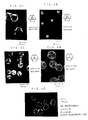
- each micrograph shows a plurality of diamond grains in a relatively small size. For this reason, the (111) oriented planes of interest may not be clearly seen.
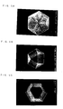
- Figs. 5A to 5C therefore, show enlarged views of three diamond grains with (111) planes having different sizes.
- Fig. 5A shows the grain with a/b ⁇ about 1/100;
- Figs. 6A to 6D are micrographs showing the sharpness of a diamond grain.
- diamond grains are isolated from each other to such an extent that the shape of each grain can be easily observed.
- new nucleation called secondary nucleation tends to occur on the polycrystalline continuous film of diamond. For this reason, it is difficult to control the orientation characteristics and shapes of grains.
- isolated grains are superior in crystallinity to a continuous film because the isolated grains have no grain boundary. Therefore, good material characteristics can be expected.
Landscapes
- Chemical & Material Sciences (AREA)
- Engineering & Computer Science (AREA)
- Crystallography & Structural Chemistry (AREA)
- Materials Engineering (AREA)
- Metallurgy (AREA)
- Organic Chemistry (AREA)
- Chemical Kinetics & Catalysis (AREA)
- General Chemical & Material Sciences (AREA)
- Crystals, And After-Treatments Of Crystals (AREA)
Applications Claiming Priority (2)
| Application Number | Priority Date | Filing Date | Title |
|---|---|---|---|
| JP7997594 | 1994-03-25 | ||
| JP79975/94 | 1994-03-25 |
Publications (2)
| Publication Number | Publication Date |
|---|---|
| EP0674028A2 true EP0674028A2 (de) | 1995-09-27 |
| EP0674028A3 EP0674028A3 (de) | 1996-04-03 |
Family
ID=13705334
Family Applications (1)
| Application Number | Title | Priority Date | Filing Date |
|---|---|---|---|
| EP95301900A Withdrawn EP0674028A3 (de) | 1994-03-25 | 1995-03-22 | Diamantkristall und Verfahren zu ihrer Herstellung. |
Country Status (3)
| Country | Link |
|---|---|
| US (2) | US5792556A (de) |
| EP (1) | EP0674028A3 (de) |
| KR (1) | KR950032732A (de) |
Cited By (3)
| Publication number | Priority date | Publication date | Assignee | Title |
|---|---|---|---|---|
| DE10027427A1 (de) * | 2000-06-02 | 2002-02-28 | Bayern Freistaat | Verfahren zur Herstellung eines Substrats mit einer an dessen Oberfläche fest anhaftenden polykristallinen Diamantschicht |
| GB2433737A (en) * | 2002-11-21 | 2007-07-04 | Element Six Ltd | A CVD single crystal diamond material |
| US8936774B2 (en) | 2002-11-21 | 2015-01-20 | Element Six Technologies Limited | Optical quality diamond material |
Families Citing this family (10)
| Publication number | Priority date | Publication date | Assignee | Title |
|---|---|---|---|---|
| US6103133A (en) * | 1997-03-19 | 2000-08-15 | Kabushiki Kaisha Toshiba | Manufacturing method of a diamond emitter vacuum micro device |
| US7309446B1 (en) | 2004-02-25 | 2007-12-18 | Metadigm Llc | Methods of manufacturing diamond capsules |
| US9470485B1 (en) | 2004-03-29 | 2016-10-18 | Victor B. Kley | Molded plastic cartridge with extended flash tube, sub-sonic cartridges, and user identification for firearms and site sensing fire control |
| JP4461110B2 (ja) * | 2006-03-14 | 2010-05-12 | 株式会社東芝 | ダイヤモンドの成膜方法 |
| US10258959B2 (en) | 2010-08-11 | 2019-04-16 | Unit Cell Diamond Llc | Methods of producing heterodiamond and apparatus therefor |
| US9783885B2 (en) | 2010-08-11 | 2017-10-10 | Unit Cell Diamond Llc | Methods for producing diamond mass and apparatus therefor |
| US9061917B2 (en) | 2010-08-11 | 2015-06-23 | Unit Cell Diamond Llc | Combinatorial synthesis of the diamond unit cell |
| US8778295B2 (en) | 2010-08-11 | 2014-07-15 | Daniel Hodes | Combinatorial synthesis of diamond |
| KR101427710B1 (ko) * | 2012-11-30 | 2014-08-13 | 한국과학기술연구원 | 기체로부터의 입자 합성을 이용한 다이아몬드 파우더의 제조 방법 및 이에 의하여 제조된 다이아몬드 파우더 |
| US9921017B1 (en) | 2013-03-15 | 2018-03-20 | Victor B. Kley | User identification for weapons and site sensing fire control |
Family Cites Families (6)
| Publication number | Priority date | Publication date | Assignee | Title |
|---|---|---|---|---|
| JPH03505861A (ja) * | 1988-06-03 | 1991-12-19 | マサチューセッツ・インステチュート・オブ・テクノロジー | ダイヤモンド上の二酸化ケイ素フィルム |
| US5082359A (en) * | 1989-11-28 | 1992-01-21 | Epion Corporation | Diamond films and method of growing diamond films on nondiamond substrates |
| US5298286A (en) * | 1992-11-09 | 1994-03-29 | North Carolina State University | Method for fabricating diamond films on nondiamond substrates and related structures |
| JP3176493B2 (ja) * | 1993-09-17 | 2001-06-18 | 株式会社神戸製鋼所 | 高配向性ダイヤモンド薄膜の形成方法 |
| JP3728464B2 (ja) * | 1994-11-25 | 2005-12-21 | 株式会社神戸製鋼所 | 単結晶ダイヤモンド膜気相合成用基板の製造方法 |
| JPH0948694A (ja) * | 1995-08-04 | 1997-02-18 | Kobe Steel Ltd | 単結晶ダイヤモンド膜の形成方法 |
-
1995
- 1995-03-22 EP EP95301900A patent/EP0674028A3/de not_active Withdrawn
- 1995-03-22 KR KR1019950006123A patent/KR950032732A/ko not_active Withdrawn
- 1995-03-24 US US08/410,218 patent/US5792556A/en not_active Expired - Fee Related
-
1997
- 1997-12-11 US US08/988,612 patent/US6060118A/en not_active Expired - Fee Related
Non-Patent Citations (3)
| Title |
|---|
| APPLIED PHYSICS LETTERS, vol. 63, no. 10, 6 September 1993 NEW YORK US, pages 1336-1338, LONG WANG ET AL 'Heteroepitaxially grown diamond on a c-BN(111) surface' * |
| EXTENDED ABSTRACTS, vol. 93/1, 1 January 1993 page 677/678 XP 000432887 YANG P C ET AL 'ORIENTED NUCLEATION OF DIAMOND FILMS ON NICKEL SUBSTRATES' * |
| THIN SOLID FILMS, vol. 238, no. 1, 15 January 1994 pages 133-140, XP 000426869 JOGENDER SINGH ET AL 'GAS FLOW EFFECTS IN SYNTHESIS OF DIAMOND BY HOT-FILAMENT CHEMICAL VAPOR DEPOSITION' * |
Cited By (8)
| Publication number | Priority date | Publication date | Assignee | Title |
|---|---|---|---|---|
| DE10027427A1 (de) * | 2000-06-02 | 2002-02-28 | Bayern Freistaat | Verfahren zur Herstellung eines Substrats mit einer an dessen Oberfläche fest anhaftenden polykristallinen Diamantschicht |
| DE10027427B4 (de) * | 2000-06-02 | 2005-09-29 | Freistaat Bayern, vertreten durch die Friedrich-Alexander-Universität Erlangen-Nürnberg | Verfahren zur Herstellung eines Substrats mit einer an dessen Oberfläche fest anhaftenden polykristallinen Diamantschicht und beschichtetes Substrat |
| GB2433737A (en) * | 2002-11-21 | 2007-07-04 | Element Six Ltd | A CVD single crystal diamond material |
| GB2433737B (en) * | 2002-11-21 | 2007-08-15 | Element Six Ltd | Optical quality diamond material |
| US8936774B2 (en) | 2002-11-21 | 2015-01-20 | Element Six Technologies Limited | Optical quality diamond material |
| US9551090B2 (en) | 2002-11-21 | 2017-01-24 | Element Six Technologies Limited | Optical quality diamond material |
| US10125434B2 (en) | 2002-11-21 | 2018-11-13 | Element Six Technologies Limited | Optical quality diamond material |
| US10851471B2 (en) | 2002-11-21 | 2020-12-01 | Element Six Technologies Limited | Optical quality diamond material |
Also Published As
| Publication number | Publication date |
|---|---|
| EP0674028A3 (de) | 1996-04-03 |
| KR950032732A (ko) | 1995-12-22 |
| US5792556A (en) | 1998-08-11 |
| US6060118A (en) | 2000-05-09 |
Similar Documents
| Publication | Publication Date | Title |
|---|---|---|
| KR910001367B1 (ko) | 기상 합성 다이아몬드막 및 그 합성방법 | |
| US5364423A (en) | Method for making diamond grit and abrasive media | |
| US6060118A (en) | CVD method of manufacturing diamond crystal | |
| Zhu et al. | Growth and characterization of diamond films on nondiamond substrates for electronic applications | |
| Zhou et al. | Control of diamond film microstructure by Ar additions to CH 4/H 2 microwave plasmas | |
| JPH08757B2 (ja) | ダイヤモンドおよびその気相合成法 | |
| EP0614998A1 (de) | Mit Diamant bedecktes Glied und Verfahren zur Herstellung | |
| US8158011B2 (en) | Method of fabrication of cubic boron nitride conical microstructures | |
| JP4294140B2 (ja) | ダイヤモンド薄膜の改質方法及びダイヤモンド薄膜の改質及び薄膜形成方法並びにダイヤモンド薄膜の加工方法 | |
| US5755879A (en) | Methods for manufacturing substrates to form monocrystalline diamond films by chemical vapor deposition | |
| EP0562574A2 (de) | Diamantkristall und Verfahren zu seiner Herstellung | |
| EP4357492A1 (de) | Diamantsubstrat und herstellungsverfahren dafür | |
| EP0371145A1 (de) | Verfahren zur herstellung von diamant aus der dampfphase | |
| Schreck | Growth of single crystal diamond wafers for future device applications | |
| National Research Council et al. | Status and applications of diamond and diamond-like materials: an emerging technology | |
| Okuyama | Cathodic needle growth from Mo (CO) 6 and Cr (CO) 6 vapors at lower electric fields | |
| JPH07309696A (ja) | ダイヤモンド結晶およびその製造方法 | |
| Kawarada et al. | Diamond synthesis by dc plasma jet cvd | |
| JPH08264862A (ja) | ダイヤモンド冷陰極およびダイヤモンド冷陰極を用いた電界放出素子ならびにダイヤモンド冷陰極の製造方法 | |
| US5492770A (en) | Method and apparatus for vapor deposition of diamond film | |
| JPH0665744A (ja) | ダイヤモンド状炭素薄膜の製造方法 | |
| JPH05139889A (ja) | ダイヤモンド結晶 | |
| Chang et al. | CVD diamond growth | |
| Gao et al. | Direct observation of atomic images of ultrathin diamond and diamond-like films | |
| JPH0959091A (ja) | ダイヤモンド結晶およびその製造方法 |
Legal Events
| Date | Code | Title | Description |
|---|---|---|---|
| PUAI | Public reference made under article 153(3) epc to a published international application that has entered the european phase |
Free format text: ORIGINAL CODE: 0009012 |
|
| AK | Designated contracting states |
Kind code of ref document: A2 Designated state(s): DE FR GB |
|
| PUAL | Search report despatched |
Free format text: ORIGINAL CODE: 0009013 |
|
| AK | Designated contracting states |
Kind code of ref document: A3 Designated state(s): DE FR GB |
|
| 17P | Request for examination filed |
Effective date: 19960507 |
|
| 17Q | First examination report despatched |
Effective date: 19960617 |
|
| STAA | Information on the status of an ep patent application or granted ep patent |
Free format text: STATUS: THE APPLICATION IS DEEMED TO BE WITHDRAWN |
|
| 18D | Application deemed to be withdrawn |
Effective date: 20000229 |