EP0674473A2 - Direktverbindung für gedruckte Schaltungen - Google Patents
Direktverbindung für gedruckte Schaltungen Download PDFInfo
- Publication number
- EP0674473A2 EP0674473A2 EP95103899A EP95103899A EP0674473A2 EP 0674473 A2 EP0674473 A2 EP 0674473A2 EP 95103899 A EP95103899 A EP 95103899A EP 95103899 A EP95103899 A EP 95103899A EP 0674473 A2 EP0674473 A2 EP 0674473A2
- Authority
- EP
- European Patent Office
- Prior art keywords
- slot
- strip
- board
- strips
- circuit board
- Prior art date
- Legal status (The legal status is an assumption and is not a legal conclusion. Google has not performed a legal analysis and makes no representation as to the accuracy of the status listed.)
- Withdrawn
Links
Images
Classifications
-
- H—ELECTRICITY
- H05—ELECTRIC TECHNIQUES NOT OTHERWISE PROVIDED FOR
- H05K—PRINTED CIRCUITS; CASINGS OR CONSTRUCTIONAL DETAILS OF ELECTRIC APPARATUS; MANUFACTURE OF ASSEMBLAGES OF ELECTRICAL COMPONENTS
- H05K3/00—Apparatus or processes for manufacturing printed circuits
- H05K3/36—Assembling printed circuits with other printed circuits
- H05K3/366—Assembling printed circuits with other printed circuits substantially perpendicularly to each other
-
- H—ELECTRICITY
- H05—ELECTRIC TECHNIQUES NOT OTHERWISE PROVIDED FOR
- H05K—PRINTED CIRCUITS; CASINGS OR CONSTRUCTIONAL DETAILS OF ELECTRIC APPARATUS; MANUFACTURE OF ASSEMBLAGES OF ELECTRICAL COMPONENTS
- H05K2201/00—Indexing scheme relating to printed circuits covered by H05K1/00
- H05K2201/04—Assemblies of printed circuits
- H05K2201/048—Second PCB mounted on first PCB by inserting in window or holes of the first PCB
-
- H—ELECTRICITY
- H05—ELECTRIC TECHNIQUES NOT OTHERWISE PROVIDED FOR
- H05K—PRINTED CIRCUITS; CASINGS OR CONSTRUCTIONAL DETAILS OF ELECTRIC APPARATUS; MANUFACTURE OF ASSEMBLAGES OF ELECTRICAL COMPONENTS
- H05K2201/00—Indexing scheme relating to printed circuits covered by H05K1/00
- H05K2201/09—Shape and layout
- H05K2201/09209—Shape and layout details of conductors
- H05K2201/095—Conductive through-holes or vias
- H05K2201/09645—Patterning on via walls; Plural lands around one hole
Definitions
- the present invention relates to electrical interconnection between separate circuit boards and particularly relates to making electrical interconnection between circuit boards of a type having the circuitry etched on a metal foil laminated on an insulating substrate or printed circuit boards as they are commonly called.
- a flexible connector such as a multiple conductor ribbon which has the opposite ends of its conductors attached to separate circuit boards which may then be stacked by bending of the flexible ribbon with the interconnection remaining intact.
- the volume of the assembled device must be maintained at a minimum, it is often cumbersome and prohibitive from a volume standpoint to stack individual circuit boards with the flexible ribbon connector extending from the sides of the stacked boards.
- the present invention provides a way or technique for directly interconnecting individual printed circuit boards in a manner which provides physical support for the interconnection with the boards extending mutually at right angles and also provides for direct electrical interconnection of the circuit strips on the individual printed circuit boards.
- the primary circuit board has an elongated slot formed therein with lug portions of the substrate material extending from the sides of the slot to a closely controlled distance oppositely spaced from each other to provide tolerance control of the width of the slot.
- the secondary printed circuit board has an insert portion thereof formed to a size and configuration to interfit the slot with the thickness of the secondary board corresponding to the width of the slot for insertion therethrough.
- the primary board has a plurality of exposed conductive strips formed on the surface thereof in spaced parallel relationship and terminating at the edge of the slot.
- the secondary board has a correspondingly disposed plurality of spaced parallel conductive strips formed thereon. Assembly insertion of the insert portion of the secondary board into the slot on the primary board is accomplished in closely fitting relationship with the long portions of the slot giving mechanical positioning support to the assembly. The adjacent ends of the conductive strips on the individual boards are then electrically interconnected by soldering, preferably by wave soldering, which bridges the slight gap therebetween.
- the present circuit board connection permits direct plug-in of a secondary board into a slot in a primary board and with the assembly thereof wave soldered for electrical interconnection and thus provides a simple economical and reliable way of connecting individual circuit boards in mass production without the need for external electrical conductors.
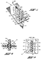
- the assembly of the present invention is indicated generally at 10 and includes a primary circuit board 12, typically a printed circuit board, which has an elongated slot 16 formed therein.
- the printed circuit board 12 is of the type having a substrate of insulating material formed with conductive film thereon portions thereof masked and etched away to form a desired circuit configuration (not shown). Although not illustrated, it will be understood that discrete components may be secured to the board 12 and any circuit thereon.
- the opposite elongated sides of the slot 16 have extending therefrom a plurality of space projections of the substrate material denoted by reference numeral 18.
- the ends of the projections 18 on opposite sides of the slot 16 terminate at a closely controlled distance from each other so as to define a slot having tightly controlled tolerances on the width of thereof. This distance is denoted by the reference character "D" in FIG. 3.
- the circuit board 12 has a plurality of spaced generally parallel conductive strips, denoted by reference numerals 20,22,24 in the drawings, provided on one side of the slot 16.
- a second plurality of spaced generally parallel strips denoted by reference numerals 26,28,30 extends on the opposite side of the slot 16 which strips are formed on the surface of the printed circuit board 12 with their ends terminating at the edges of the slot 16 intermediate the projections 18.
- each of the strips such as strips 20,22,24,26,28,30 on the upper surface of the primary board 12 may have a counterpart strip located directly below on the undersurface of the board as denoted by reference numerals 20',22',24',26',28',30' in FIGS. 1 and 2. It will be understood however, that the counterpart strips 20',22',24',26',28',30' are not necessary for the practice of the invention.
- the secondary board 14 likewise has a plurality of conductive strips disposed thereon in spaced generally parallel relationship on the insert portion of the board which is denoted by reference numeral 32 and which strips are denoted by reference numerals 34,36,38 on the front side of the board portion 32.
- Preferably counterpart strips denoted with corresponding primed numerals are provided on the opposite face thereof.
- the strips on the portion 32 of member 14 are disposed oppositely in pairs at a common station thereon such as the pair 36, 36' and are interconnected through a hole or "via" aperture 40 formed through the insulating substrate material which permits the metal conductor when plated on the board 14 to be deposited in the via aperture and interconnect the strips 36, 36'.
- strips 34 and its oppositely disposed strip 34' which is shown only in dashed outline are interconnected, as are strip 38 and its oppositely disposed strip 38' which is shown only in dashed outline.
- FIG. 2 illustrates typically the electrical connection between strip 36 and the strips 22, 22' and the electrical connection between strip 36' and the strips 28, 28'. It will be understood that strips 20',22',24' and 26',28',30' may be omitted and are not essential for the practice of the invention.
- the present invention thus provides for direct plug-in connection of individual circuit boards by insertion of a portion of one sized and configured to closely interfit a slot in the other board with strips provided on each board terminating closely spaced and adjacent and which are subsequently electrically interconnected by soldering.
Landscapes
- Engineering & Computer Science (AREA)
- Manufacturing & Machinery (AREA)
- Microelectronics & Electronic Packaging (AREA)
- Combinations Of Printed Boards (AREA)
- Coupling Device And Connection With Printed Circuit (AREA)
- Multi-Conductor Connections (AREA)
Applications Claiming Priority (2)
| Application Number | Priority Date | Filing Date | Title |
|---|---|---|---|
| US08/215,337 US5455742A (en) | 1994-03-21 | 1994-03-21 | Direct circuit board connection |
| US215337 | 2002-08-08 |
Publications (2)
| Publication Number | Publication Date |
|---|---|
| EP0674473A2 true EP0674473A2 (de) | 1995-09-27 |
| EP0674473A3 EP0674473A3 (de) | 1996-01-03 |
Family
ID=22802589
Family Applications (1)
| Application Number | Title | Priority Date | Filing Date |
|---|---|---|---|
| EP95103899A Withdrawn EP0674473A3 (de) | 1994-03-21 | 1995-03-16 | Direktverbindung für gedruckte Schaltungen. |
Country Status (4)
| Country | Link |
|---|---|
| US (1) | US5455742A (de) |
| EP (1) | EP0674473A3 (de) |
| JP (1) | JPH07273444A (de) |
| CA (1) | CA2144247C (de) |
Cited By (2)
| Publication number | Priority date | Publication date | Assignee | Title |
|---|---|---|---|---|
| EP0766507A1 (de) | 1995-09-12 | 1997-04-02 | Allen-Bradley Company, Inc. | Leiterplatte mit einer Öffnung zum Aufnehmen eines Single-in-Line-packungsmoduls |
| DE19838218A1 (de) * | 1998-08-22 | 2000-02-24 | Insta Elektro Gmbh & Co Kg | Konstruktive Anordnung zweier Leiterplatten in einem elektrischen Installationsgerät zum Einbau in genormte Installationsdosen |
Families Citing this family (28)
| Publication number | Priority date | Publication date | Assignee | Title |
|---|---|---|---|---|
| US5648892A (en) * | 1995-09-29 | 1997-07-15 | Allen-Bradley Company, Inc. | Wireless circuit board system for a motor controller |
| US6042390A (en) * | 1995-12-01 | 2000-03-28 | Asante Technologies, Inc. | Network hub interconnection component |
| US5907475A (en) * | 1996-04-16 | 1999-05-25 | Allen-Bradley Company, Llc | Circuit board system having a mounted board and a plurality of mounting boards |
| JPH10209594A (ja) * | 1997-01-17 | 1998-08-07 | Fuji Photo Optical Co Ltd | フレキシブルプリント回路基板と硬質プリント回路基板との接続構造 |
| US6004140A (en) * | 1997-10-09 | 1999-12-21 | Denso Corporation | Female electric connector |
| US6594152B2 (en) * | 1999-09-30 | 2003-07-15 | Intel Corporation | Board-to-board electrical coupling with conductive band |
| US6533587B1 (en) * | 2000-07-05 | 2003-03-18 | Network Engines, Inc. | Circuit board riser |
| US6528737B1 (en) * | 2000-08-16 | 2003-03-04 | Nortel Networks Limited | Midplane configuration featuring surface contact connectors |
| US6496384B1 (en) * | 2001-09-21 | 2002-12-17 | Visteon Global Technologies, Inc. | Circuit board assembly and method of fabricating same |
| US6965279B2 (en) * | 2003-07-18 | 2005-11-15 | Ems Technologies, Inc. | Double-sided, edge-mounted stripline signal processing modules and modular network |
| US6984156B2 (en) * | 2003-09-05 | 2006-01-10 | Power-One Limited | Connector for surface mounting subassemblies vertically on a mother board and assemblies comprising the same |
| US6918775B2 (en) * | 2003-09-23 | 2005-07-19 | Hon Hai Precision Ind. Co., Ltd. | Method for interconnecting multiple printed circuit boards |
| TW200529497A (en) * | 2004-02-24 | 2005-09-01 | Hon Hai Prec Ind Co Ltd | Method for interconnecting multiple printed circuit boards |
| KR20060064924A (ko) * | 2004-12-09 | 2006-06-14 | 삼성전자주식회사 | 하이브리드 회로기판 및 이를 갖는 표시장치 |
| WO2009066391A1 (ja) * | 2007-11-22 | 2009-05-28 | Fujitsu Limited | プリント基板およびその製造方法 |
| US7716821B2 (en) * | 2007-12-12 | 2010-05-18 | Sauer-Danfoss Inc. | Method of manufacturing a circuit board assembly for a controller |
| FR2928066A1 (fr) * | 2008-02-27 | 2009-08-28 | Thomson Licensing Sas | Systeme d'interconnexion de deux substrats comportant chacun au moins une ligne de transmission |
| JP5258123B2 (ja) * | 2009-11-20 | 2013-08-07 | 日本航空電子工業株式会社 | コネクタ及び照明装置 |
| US9648744B2 (en) * | 2012-07-24 | 2017-05-09 | Apple Inc. | Ejectable component assemblies in electronic devices |
| CN102821546A (zh) * | 2012-09-03 | 2012-12-12 | 威海华菱光电股份有限公司 | 接触式图像传感器的电路板组件及其制造方法 |
| EP3146811B1 (de) * | 2014-05-22 | 2023-08-02 | Signify Holding B.V. | Leiterplattenanordnung |
| US10608359B2 (en) * | 2016-12-16 | 2020-03-31 | Samsung Electronics Co., Ltd. | Connection structure between flat cable and electronic circuit board |
| CN106704993A (zh) * | 2017-01-09 | 2017-05-24 | 宁波亚茂光电股份有限公司 | 一种插卡式电源与光源板的连接结构 |
| WO2019087352A1 (ja) * | 2017-11-02 | 2019-05-09 | 三菱電機株式会社 | プリント基板組立体 |
| JP6925447B2 (ja) * | 2017-12-08 | 2021-08-25 | 三菱電機株式会社 | プリント配線板およびその製造方法 |
| EP3829271A4 (de) * | 2018-07-26 | 2021-09-29 | Mitsubishi Electric Corporation | Leiterplatte |
| CA3107141C (en) * | 2018-07-26 | 2023-01-24 | Mitsubishi Electric Corporation | Printed circuit board |
| EP4125310A1 (de) * | 2021-07-29 | 2023-02-01 | Aptiv Technologies Limited | Leiterplattenverbindungssystem, vorrichtung und verfahren |
Family Cites Families (4)
| Publication number | Priority date | Publication date | Assignee | Title |
|---|---|---|---|---|
| US2707272A (en) * | 1954-05-21 | 1955-04-26 | Sanders Associates Inc | Mounting device for electric components |
| US3200020A (en) * | 1963-12-23 | 1965-08-10 | Gen Precision Inc | Method of making a weldable printed circuit |
| US3624587A (en) * | 1970-02-09 | 1971-11-30 | Litton Systems Inc | Clinched-wire interconnection device for printed circuit boards |
| DE4323827C1 (de) * | 1993-07-15 | 1994-12-08 | Siemens Ag | Steckbare Baugruppe |
-
1994
- 1994-03-21 US US08/215,337 patent/US5455742A/en not_active Expired - Lifetime
-
1995
- 1995-03-09 CA CA002144247A patent/CA2144247C/en not_active Expired - Fee Related
- 1995-03-16 EP EP95103899A patent/EP0674473A3/de not_active Withdrawn
- 1995-03-20 JP JP7061019A patent/JPH07273444A/ja active Pending
Cited By (2)
| Publication number | Priority date | Publication date | Assignee | Title |
|---|---|---|---|---|
| EP0766507A1 (de) | 1995-09-12 | 1997-04-02 | Allen-Bradley Company, Inc. | Leiterplatte mit einer Öffnung zum Aufnehmen eines Single-in-Line-packungsmoduls |
| DE19838218A1 (de) * | 1998-08-22 | 2000-02-24 | Insta Elektro Gmbh & Co Kg | Konstruktive Anordnung zweier Leiterplatten in einem elektrischen Installationsgerät zum Einbau in genormte Installationsdosen |
Also Published As
| Publication number | Publication date |
|---|---|
| EP0674473A3 (de) | 1996-01-03 |
| CA2144247C (en) | 1999-09-14 |
| CA2144247A1 (en) | 1995-09-22 |
| US5455742A (en) | 1995-10-03 |
| JPH07273444A (ja) | 1995-10-20 |
Similar Documents
| Publication | Publication Date | Title |
|---|---|---|
| CA2144247C (en) | Direct circuit board connection | |
| EP0677213B1 (de) | Verbindungssystem | |
| EP0197623A2 (de) | Elektrische Mehrleiterverbinder und Verfahren zu deren Herstellung | |
| US20060128197A1 (en) | Board mounted power connector | |
| EP0657960A2 (de) | Leiterplattenverbinder | |
| EP1538716A2 (de) | Elektrischer Verbinder mit Leiterplattenbaugruppen | |
| US4385791A (en) | Electrical adaptor block | |
| US20090034222A1 (en) | Printed circuit board assembly and method of making a printed circuit board | |
| EP0028491B1 (de) | Elektrischer Verbinder zum Montieren eines flachen Wandlers auf einer gedruckten Schaltungskarte | |
| US4343084A (en) | Method for making printed circuit boards with connector terminals | |
| US6135816A (en) | Electrical connector having an improved construction for fixing shield plates to a receptacle connector | |
| EP0017358A1 (de) | Elektrisches Steckergehäuse mit einem Befestigungsstift | |
| US7112072B2 (en) | Ground bus for an electrical connector | |
| JPH07297562A (ja) | ジャンクションボックス及びその基板組立体 | |
| EP1473802B1 (de) | Steckkontakt | |
| US6692273B1 (en) | Straddle mount connector | |
| IE990128A1 (en) | Right Angle Electrical Connector | |
| GB2242579A (en) | Electrical connectors for flat insulated boards | |
| EP1969684A2 (de) | Elektrische verbinderbaugruppe und herstellungsverfahren dafür | |
| EP0132327A2 (de) | Ein flaches elektronisches Filterelement und ein mit solchen Filtern versehener Verbinder | |
| JP3824352B2 (ja) | 電気コネクタ | |
| US6116948A (en) | Electrical connector for terminating discrete electrical wires | |
| GB2154077A (en) | Connecting a flexible circuit to a rigid circuit board | |
| US3040214A (en) | Printed circuit capacitor and method of manufacture | |
| GB2069249A (en) | Multi-way electrical connectors |
Legal Events
| Date | Code | Title | Description |
|---|---|---|---|
| PUAI | Public reference made under article 153(3) epc to a published international application that has entered the european phase |
Free format text: ORIGINAL CODE: 0009012 |
|
| AK | Designated contracting states |
Kind code of ref document: A2 Designated state(s): DE FR GB |
|
| PUAL | Search report despatched |
Free format text: ORIGINAL CODE: 0009013 |
|
| AK | Designated contracting states |
Kind code of ref document: A3 Designated state(s): DE FR GB |
|
| STAA | Information on the status of an ep patent application or granted ep patent |
Free format text: STATUS: THE APPLICATION IS DEEMED TO BE WITHDRAWN |
|
| 18D | Application deemed to be withdrawn |
Effective date: 19960704 |