EP0675559A1 - Commutateur pour le domaine des hautes fréquences - Google Patents
Commutateur pour le domaine des hautes fréquences Download PDFInfo
- Publication number
- EP0675559A1 EP0675559A1 EP95104168A EP95104168A EP0675559A1 EP 0675559 A1 EP0675559 A1 EP 0675559A1 EP 95104168 A EP95104168 A EP 95104168A EP 95104168 A EP95104168 A EP 95104168A EP 0675559 A1 EP0675559 A1 EP 0675559A1
- Authority
- EP
- European Patent Office
- Prior art keywords
- output
- diodes
- switching
- branch
- switched
- Prior art date
- Legal status (The legal status is an assumption and is not a legal conclusion. Google has not performed a legal analysis and makes no representation as to the accuracy of the status listed.)
- Granted
Links
- 239000004065 semiconductor Substances 0.000 claims abstract 2
- 230000000903 blocking effect Effects 0.000 claims description 2
- 238000002955 isolation Methods 0.000 description 4
- 238000003780 insertion Methods 0.000 description 3
- 230000037431 insertion Effects 0.000 description 3
- 238000005516 engineering process Methods 0.000 description 2
- 239000000758 substrate Substances 0.000 description 2
- 239000000919 ceramic Substances 0.000 description 1
- 238000010276 construction Methods 0.000 description 1
- 238000011161 development Methods 0.000 description 1
- 230000018109 developmental process Effects 0.000 description 1
- 230000000694 effects Effects 0.000 description 1
- 230000001939 inductive effect Effects 0.000 description 1
- 238000009413 insulation Methods 0.000 description 1
Images
Classifications
-
- H—ELECTRICITY
- H01—ELECTRIC ELEMENTS
- H01P—WAVEGUIDES; RESONATORS, LINES, OR OTHER DEVICES OF THE WAVEGUIDE TYPE
- H01P1/00—Auxiliary devices
- H01P1/10—Auxiliary devices for switching or interrupting
- H01P1/15—Auxiliary devices for switching or interrupting by semiconductor devices
Definitions
- the invention relates to a switch for the high frequency range according to the preamble of claim 1.
- Such switches include an input gate and two output gates and have the effect that a high-frequency signal (RF signal) coupled into the input gate can alternatively be switched to one of the output gates as a function of a control signal.
- RF signal high-frequency signal
- Such switches are used in particular in radar technology in so-called T / R modules and are used in this Field of application also called SPDT switch (" S ingle P ole D ouble T hrow").
- SPDT switch S ingle P ole D ouble T hrow
- Such SPDT switches are for the maximum frequency range, for. B. designed the gigahertz (GHz) range.
- the invention has for its object to provide a generic switch that enables the lossless switching of an RF signal with high power, with the highest possible isolation in the blocked branch and between the output gates and which can be produced in a cost-effective and reliable manner.
- a first advantage of the invention is that in the X-band range (approximately 10 GHz) a structure with a power compatibility greater than or equal to 20 watts with an insertion loss in the switched branch of less than or equal to 1.0 dB and an insulation in the blocked branch greater than or equal 30 dB, isolation between the output gates greater than or equal to 30 dB and a standing wave ratio VSWR at all gates less than or equal to 2: 1 is possible.
- a second advantage is that a mechanically compact and robust construction is possible in hybrid circuit technology.
- a third advantage is that the diodes required for switching, e.g. PIN diodes are not directly in the RF signal path.
- the non-blocking (switched through) branch can have a very high RF power, for example 25 W, with very little insertion loss.
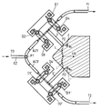
- the figure shows an exemplary circuit arrangement, which on a substrate, for. B. a ceramic substrate for a frequency range of z. B. 8 GHz can be produced.
- the arrangement contains a y-shaped waveguide which is adapted to the specified frequency range and the RF power to be switched, the input branch EZ of which is coupled to the input gate TO and which branches at a branching point P1 into the two output branches AZ1, AZ2.
- Each output branch AZ1, AZ2 contains a switchable filter for the specified frequency range, for example a band or low-pass filter.
- the diodes D1 to D4 and D1 'to D4' preferably consist of PIN diodes for the specified HF range.
- Two diode quartets D1 to D4 and D1 'to D4' are created. Each diode quartet contains two diode pairs D1, D4 and D2, D3 and D1 ', D4' and D2 ', D3'. For each pair of diodes, the associated diodes are on opposite sides of the associated output waveguide.
- each diode quartet similar connections, for example anodes, are connected to the associated output waveguide, while the other connections (cathodes) are at reference potential (ground).
- the diodes are polarized in opposite directions, so that depending on the switching voltage UB a filter, e.g. B. in the output branch AZ1, can be switched into the pass band, while the other filter, for. B. in the output branch AZ2, is switched to the locked state.
- a filter e.g. B. in the output branch AZ1
- the other filter for. B. in the output branch AZ2
- the diodes are connected in opposite directions. This advantageously means that only a single switching voltage UB is required, which enables the filters in the output branches to always have opposite switching states for the RF signal.
- a type of circuit polarity of the respective diode quartet can be set by selecting the spacing of the diode pairs within a diode quartet depending on the frequency range used. For example, it is possible to choose the distance between the two diode pairs in such a way that, in the case of high-resistance diodes (for the HF signal), this becomes transparent within a diode quartet for the prevailing RF signal, that is, the filter is switched to the on state. In the blocked state, each filter acts as a short circuit for the RF signal.
- This short circuit is transformed in such a way that there is an open circuit for the relevant output branch at the branching point P1.
- the RF power coupled into the input branch EZ is then advantageously conducted almost losslessly into the respective other output branch to the corresponding output gate.
- the switching voltage UB a direct voltage, causes a direct current which is supplied to the switching points P2, P2 'via filters L, C or L', C '. These are coupled to the associated diode quartets via a line S or S ', which is also a component determining the filter.
- the arrangement described also has the advantage that through the switchable filters present in the output branches AZ1, AZ2, the z. B. are carried out in a so-called quasi-lumped element design, in the RF signal at the input gate TO possibly existing harmonics are suppressed.
- an insertion loss of less than or equal to 0.6 dB can be achieved in continuous operation with an RF power of greater than or equal to 20 watts (measured between an unlocked output gate and the Entrance gate TO).
- the RF isolation in the blocked output branch is greater than 35 dB.
- the RF isolation between the output gates T1, T2 is greater than 35 dB.
- the invention is not limited to the example described, but can be applied analogously to others.
- it is known to a person skilled in the art to choose a waveguide structure matched to it and corresponding switching diodes (diode quartets) for each RF range to be selected.
Landscapes
- Waveguide Switches, Polarizers, And Phase Shifters (AREA)
- Electronic Switches (AREA)
Applications Claiming Priority (4)
| Application Number | Priority Date | Filing Date | Title |
|---|---|---|---|
| DE4411250 | 1994-03-31 | ||
| DE4411250 | 1994-03-31 | ||
| DE19503300 | 1995-02-02 | ||
| DE19503300A DE19503300A1 (de) | 1994-03-31 | 1995-02-02 | Umschalter für den Hochfrequenzbereich |
Publications (2)
| Publication Number | Publication Date |
|---|---|
| EP0675559A1 true EP0675559A1 (fr) | 1995-10-04 |
| EP0675559B1 EP0675559B1 (fr) | 2000-05-24 |
Family
ID=25935275
Family Applications (1)
| Application Number | Title | Priority Date | Filing Date |
|---|---|---|---|
| EP19950104168 Expired - Lifetime EP0675559B1 (fr) | 1994-03-31 | 1995-03-22 | Commutateur pour le domaine des hautes fréquences |
Country Status (1)
| Country | Link |
|---|---|
| EP (1) | EP0675559B1 (fr) |
Citations (2)
| Publication number | Priority date | Publication date | Assignee | Title |
|---|---|---|---|---|
| US4078217A (en) * | 1976-04-05 | 1978-03-07 | The United States Of America As Represented By The Secretary Of The Navy | Microwave isolation switch |
| US4502027A (en) * | 1982-03-01 | 1985-02-26 | Raytheon Company | Bidirectional switch |
-
1995
- 1995-03-22 EP EP19950104168 patent/EP0675559B1/fr not_active Expired - Lifetime
Patent Citations (2)
| Publication number | Priority date | Publication date | Assignee | Title |
|---|---|---|---|---|
| US4078217A (en) * | 1976-04-05 | 1978-03-07 | The United States Of America As Represented By The Secretary Of The Navy | Microwave isolation switch |
| US4502027A (en) * | 1982-03-01 | 1985-02-26 | Raytheon Company | Bidirectional switch |
Non-Patent Citations (1)
| Title |
|---|
| G.H. NESBIT ET AL.: "Monolithic transmit/receive switch for millimeter-wave application", GAAS IC SYMPOSIUM 1987,TECHNICAL DIGEST;PORTLAND,US, 13 October 1987 (1987-10-13) - 16 October 1987 (1987-10-16), pages 147 - 148 * |
Also Published As
| Publication number | Publication date |
|---|---|
| EP0675559B1 (fr) | 2000-05-24 |
Similar Documents
| Publication | Publication Date | Title |
|---|---|---|
| DE2645898C2 (fr) | ||
| DE68907613T2 (de) | Anordnung mit bandsperrfiltern. | |
| DE112012002264B4 (de) | Hochfrequenzschalter | |
| DE19909521A1 (de) | Elektronischer einpoliger Umschalter | |
| DE69005075T2 (de) | Hybrider Schalter mit GaAs-MMIC-FET und PIN-Diode. | |
| DE2645899A1 (de) | Phasenschieber in form einer pi-schaltung | |
| DE68922177T2 (de) | Schaltungsanordnung für Funkempfänger. | |
| DE69307412T2 (de) | Antennenumschaltanordnung zum Selektiven Verbinden einer Antenne mit einem Sender oder einem Empfänger | |
| DE3712003A1 (de) | Schalt-schaltungsanordnung | |
| DE2255207A1 (de) | Anordnung zum ableiten des fehlersignals in einem system zum selbsttaetigen nachfuehren einer mikrowellenantenne | |
| DE2058485C3 (de) | Anordnung für die Umschaltung und Verteilung von Hochfrequenz-Energie | |
| DE10100559B4 (de) | Einfachsymmetrischer Mischer | |
| DE3202329C2 (fr) | ||
| DE4341301C2 (de) | Vielfach-Bit-Phasenschieber | |
| DE60101089T2 (de) | Multifunktionelle integrierte schaltungsanordnung hoher frequenz | |
| DE3817772A1 (de) | Phasenschieberkombinator | |
| DE2518306C3 (de) | Amplitudenbegrenzer | |
| EP0675559B1 (fr) | Commutateur pour le domaine des hautes fréquences | |
| DE19635175A1 (de) | Telekommunikationsgerät mit als Ringschaltung ausgeführter Schaltvorrichtung | |
| DE3324540C2 (de) | Breitbandiger Mikrowellenverstärker | |
| DE19731085A1 (de) | Einrichtung zum Senden und Empfangen von Radarwellen, insbesondere für einen Abstandssensor | |
| DE19902346A1 (de) | Kopplungsstruktur als Signalschalter | |
| DE3507779A1 (de) | Ueberlastschutz fuer hf-empfaenger | |
| DE19503300A1 (de) | Umschalter für den Hochfrequenzbereich | |
| EP0328013B1 (fr) | Commutateur électrique pour guides d'ondes |
Legal Events
| Date | Code | Title | Description |
|---|---|---|---|
| PUAI | Public reference made under article 153(3) epc to a published international application that has entered the european phase |
Free format text: ORIGINAL CODE: 0009012 |
|
| AK | Designated contracting states |
Kind code of ref document: A1 Designated state(s): DE FR GB NL |
|
| 17P | Request for examination filed |
Effective date: 19960320 |
|
| 17Q | First examination report despatched |
Effective date: 19971203 |
|
| GRAG | Despatch of communication of intention to grant |
Free format text: ORIGINAL CODE: EPIDOS AGRA |
|
| GRAG | Despatch of communication of intention to grant |
Free format text: ORIGINAL CODE: EPIDOS AGRA |
|
| GRAH | Despatch of communication of intention to grant a patent |
Free format text: ORIGINAL CODE: EPIDOS IGRA |
|
| GRAH | Despatch of communication of intention to grant a patent |
Free format text: ORIGINAL CODE: EPIDOS IGRA |
|
| RAP1 | Party data changed (applicant data changed or rights of an application transferred) |
Owner name: DAIMLERCHRYSLER AEROSPACE AG |
|
| GRAA | (expected) grant |
Free format text: ORIGINAL CODE: 0009210 |
|
| AK | Designated contracting states |
Kind code of ref document: B1 Designated state(s): DE FR GB NL |
|
| REF | Corresponds to: |
Ref document number: 59508368 Country of ref document: DE Date of ref document: 20000629 |
|
| GBT | Gb: translation of ep patent filed (gb section 77(6)(a)/1977) |
Effective date: 20000627 |
|
| ET | Fr: translation filed | ||
| PLBE | No opposition filed within time limit |
Free format text: ORIGINAL CODE: 0009261 |
|
| STAA | Information on the status of an ep patent application or granted ep patent |
Free format text: STATUS: NO OPPOSITION FILED WITHIN TIME LIMIT |
|
| 26N | No opposition filed | ||
| REG | Reference to a national code |
Ref country code: GB Ref legal event code: IF02 |
|
| PGFP | Annual fee paid to national office [announced via postgrant information from national office to epo] |
Ref country code: DE Payment date: 20130321 Year of fee payment: 19 Ref country code: FR Payment date: 20130408 Year of fee payment: 19 Ref country code: GB Payment date: 20130321 Year of fee payment: 19 |
|
| PGFP | Annual fee paid to national office [announced via postgrant information from national office to epo] |
Ref country code: NL Payment date: 20130320 Year of fee payment: 19 |
|
| REG | Reference to a national code |
Ref country code: DE Ref legal event code: R119 Ref document number: 59508368 Country of ref document: DE |
|
| REG | Reference to a national code |
Ref country code: NL Ref legal event code: V1 Effective date: 20141001 |
|
| GBPC | Gb: european patent ceased through non-payment of renewal fee |
Effective date: 20140322 |
|
| REG | Reference to a national code |
Ref country code: FR Ref legal event code: ST Effective date: 20141128 |
|
| REG | Reference to a national code |
Ref country code: DE Ref legal event code: R119 Ref document number: 59508368 Country of ref document: DE Effective date: 20141001 |
|
| PG25 | Lapsed in a contracting state [announced via postgrant information from national office to epo] |
Ref country code: FR Free format text: LAPSE BECAUSE OF NON-PAYMENT OF DUE FEES Effective date: 20140331 Ref country code: DE Free format text: LAPSE BECAUSE OF NON-PAYMENT OF DUE FEES Effective date: 20141001 Ref country code: GB Free format text: LAPSE BECAUSE OF NON-PAYMENT OF DUE FEES Effective date: 20140322 |
|
| PG25 | Lapsed in a contracting state [announced via postgrant information from national office to epo] |
Ref country code: NL Free format text: LAPSE BECAUSE OF NON-PAYMENT OF DUE FEES Effective date: 20141001 |