EP0676749A2 - Dispositif et méthode de reproduction d'information - Google Patents
Dispositif et méthode de reproduction d'information Download PDFInfo
- Publication number
- EP0676749A2 EP0676749A2 EP95201397A EP95201397A EP0676749A2 EP 0676749 A2 EP0676749 A2 EP 0676749A2 EP 95201397 A EP95201397 A EP 95201397A EP 95201397 A EP95201397 A EP 95201397A EP 0676749 A2 EP0676749 A2 EP 0676749A2
- Authority
- EP
- European Patent Office
- Prior art keywords
- recording medium
- recording
- light
- information
- optical probe
- Prior art date
- Legal status (The legal status is an assumption and is not a legal conclusion. Google has not performed a legal analysis and makes no representation as to the accuracy of the status listed.)
- Granted
Links
- 238000000034 method Methods 0.000 title claims description 7
- 239000000523 sample Substances 0.000 claims abstract description 44
- 230000003287 optical effect Effects 0.000 claims abstract description 36
- 239000000758 substrate Substances 0.000 claims abstract description 23
- 230000001678 irradiating effect Effects 0.000 claims abstract description 13
- 238000002835 absorbance Methods 0.000 claims description 9
- 230000010365 information processing Effects 0.000 description 15
- 239000000463 material Substances 0.000 description 8
- 238000004574 scanning tunneling microscopy Methods 0.000 description 8
- 230000015654 memory Effects 0.000 description 7
- 238000003672 processing method Methods 0.000 description 7
- 238000004647 photon scanning tunneling microscopy Methods 0.000 description 5
- 238000002347 injection Methods 0.000 description 4
- 239000007924 injection Substances 0.000 description 4
- 238000010521 absorption reaction Methods 0.000 description 3
- LLCSWKVOHICRDD-UHFFFAOYSA-N buta-1,3-diyne Chemical group C#CC#C LLCSWKVOHICRDD-UHFFFAOYSA-N 0.000 description 3
- 238000001514 detection method Methods 0.000 description 3
- 238000011161 development Methods 0.000 description 3
- 230000018109 developmental process Effects 0.000 description 3
- 239000011521 glass Substances 0.000 description 3
- 239000013307 optical fiber Substances 0.000 description 3
- 229920000642 polymer Polymers 0.000 description 3
- 239000004065 semiconductor Substances 0.000 description 3
- 230000004304 visual acuity Effects 0.000 description 3
- XEEYBQQBJWHFJM-UHFFFAOYSA-N Iron Chemical compound [Fe] XEEYBQQBJWHFJM-UHFFFAOYSA-N 0.000 description 2
- KDLHZDBZIXYQEI-UHFFFAOYSA-N Palladium Chemical compound [Pd] KDLHZDBZIXYQEI-UHFFFAOYSA-N 0.000 description 2
- 230000003321 amplification Effects 0.000 description 2
- 239000010408 film Substances 0.000 description 2
- 230000031700 light absorption Effects 0.000 description 2
- 238000003199 nucleic acid amplification method Methods 0.000 description 2
- 239000010409 thin film Substances 0.000 description 2
- XOLBLPGZBRYERU-UHFFFAOYSA-N tin dioxide Chemical compound O=[Sn]=O XOLBLPGZBRYERU-UHFFFAOYSA-N 0.000 description 2
- 101100006523 Arabidopsis thaliana CHC2 gene Proteins 0.000 description 1
- RYGMFSIKBFXOCR-UHFFFAOYSA-N Copper Chemical compound [Cu] RYGMFSIKBFXOCR-UHFFFAOYSA-N 0.000 description 1
- 239000004642 Polyimide Substances 0.000 description 1
- 239000004020 conductor Substances 0.000 description 1
- 229910052802 copper Inorganic materials 0.000 description 1
- 239000010949 copper Substances 0.000 description 1
- 238000010586 diagram Methods 0.000 description 1
- 230000000694 effects Effects 0.000 description 1
- 230000005251 gamma ray Effects 0.000 description 1
- CPBQJMYROZQQJC-UHFFFAOYSA-N helium neon Chemical compound [He].[Ne] CPBQJMYROZQQJC-UHFFFAOYSA-N 0.000 description 1
- 229910052742 iron Inorganic materials 0.000 description 1
- 239000000696 magnetic material Substances 0.000 description 1
- 229910052751 metal Inorganic materials 0.000 description 1
- 239000002184 metal Substances 0.000 description 1
- JKQOBWVOAYFWKG-UHFFFAOYSA-N molybdenum trioxide Inorganic materials O=[Mo](=O)=O JKQOBWVOAYFWKG-UHFFFAOYSA-N 0.000 description 1
- 229910052763 palladium Inorganic materials 0.000 description 1
- 238000005498 polishing Methods 0.000 description 1
- 229920001721 polyimide Polymers 0.000 description 1
- 238000012545 processing Methods 0.000 description 1
- 230000004044 response Effects 0.000 description 1
- 230000003595 spectral effect Effects 0.000 description 1
- 239000000126 substance Substances 0.000 description 1
- PCCVSPMFGIFTHU-UHFFFAOYSA-N tetracyanoquinodimethane Chemical compound N#CC(C#N)=C1C=CC(=C(C#N)C#N)C=C1 PCCVSPMFGIFTHU-UHFFFAOYSA-N 0.000 description 1
Images
Classifications
-
- G—PHYSICS
- G11—INFORMATION STORAGE
- G11B—INFORMATION STORAGE BASED ON RELATIVE MOVEMENT BETWEEN RECORD CARRIER AND TRANSDUCER
- G11B7/00—Recording or reproducing by optical means, e.g. recording using a thermal beam of optical radiation by modifying optical properties or the physical structure, reproducing using an optical beam at lower power by sensing optical properties; Record carriers therefor
- G11B7/004—Recording, reproducing or erasing methods; Read, write or erase circuits therefor
- G11B7/005—Reproducing
-
- G—PHYSICS
- G11—INFORMATION STORAGE
- G11B—INFORMATION STORAGE BASED ON RELATIVE MOVEMENT BETWEEN RECORD CARRIER AND TRANSDUCER
- G11B11/00—Recording on or reproducing from the same record carrier wherein for these two operations the methods are covered by different main groups of groups G11B3/00 - G11B7/00 or by different subgroups of group G11B9/00; Record carriers therefor
-
- G—PHYSICS
- G11—INFORMATION STORAGE
- G11B—INFORMATION STORAGE BASED ON RELATIVE MOVEMENT BETWEEN RECORD CARRIER AND TRANSDUCER
- G11B7/00—Recording or reproducing by optical means, e.g. recording using a thermal beam of optical radiation by modifying optical properties or the physical structure, reproducing using an optical beam at lower power by sensing optical properties; Record carriers therefor
- G11B7/004—Recording, reproducing or erasing methods; Read, write or erase circuits therefor
- G11B7/0045—Recording
- G11B7/00455—Recording involving reflectivity, absorption or colour changes
-
- G—PHYSICS
- G11—INFORMATION STORAGE
- G11B—INFORMATION STORAGE BASED ON RELATIVE MOVEMENT BETWEEN RECORD CARRIER AND TRANSDUCER
- G11B7/00—Recording or reproducing by optical means, e.g. recording using a thermal beam of optical radiation by modifying optical properties or the physical structure, reproducing using an optical beam at lower power by sensing optical properties; Record carriers therefor
- G11B7/004—Recording, reproducing or erasing methods; Read, write or erase circuits therefor
- G11B7/005—Reproducing
- G11B7/0052—Reproducing involving reflectivity, absorption or colour changes
-
- G—PHYSICS
- G11—INFORMATION STORAGE
- G11B—INFORMATION STORAGE BASED ON RELATIVE MOVEMENT BETWEEN RECORD CARRIER AND TRANSDUCER
- G11B7/00—Recording or reproducing by optical means, e.g. recording using a thermal beam of optical radiation by modifying optical properties or the physical structure, reproducing using an optical beam at lower power by sensing optical properties; Record carriers therefor
- G11B7/12—Heads, e.g. forming of the optical beam spot or modulation of the optical beam
- G11B7/135—Means for guiding the beam from the source to the record carrier or from the record carrier to the detector
- G11B7/1384—Fibre optics
-
- G—PHYSICS
- G11—INFORMATION STORAGE
- G11B—INFORMATION STORAGE BASED ON RELATIVE MOVEMENT BETWEEN RECORD CARRIER AND TRANSDUCER
- G11B9/00—Recording or reproducing using a method not covered by one of the main groups G11B3/00 - G11B7/00; Record carriers therefor
- G11B9/12—Recording or reproducing using a method not covered by one of the main groups G11B3/00 - G11B7/00; Record carriers therefor using near-field interactions; Record carriers therefor
- G11B9/14—Recording or reproducing using a method not covered by one of the main groups G11B3/00 - G11B7/00; Record carriers therefor using near-field interactions; Record carriers therefor using microscopic probe means, i.e. recording or reproducing by means directly associated with the tip of a microscopic electrical probe as used in Scanning Tunneling Microscopy [STM] or Atomic Force Microscopy [AFM] for inducing physical or electrical perturbations in a recording medium; Record carriers or media specially adapted for such transducing of information
-
- B—PERFORMING OPERATIONS; TRANSPORTING
- B82—NANOTECHNOLOGY
- B82Y—SPECIFIC USES OR APPLICATIONS OF NANOSTRUCTURES; MEASUREMENT OR ANALYSIS OF NANOSTRUCTURES; MANUFACTURE OR TREATMENT OF NANOSTRUCTURES
- B82Y10/00—Nanotechnology for information processing, storage or transmission, e.g. quantum computing or single electron logic
-
- B—PERFORMING OPERATIONS; TRANSPORTING
- B82—NANOTECHNOLOGY
- B82Y—SPECIFIC USES OR APPLICATIONS OF NANOSTRUCTURES; MEASUREMENT OR ANALYSIS OF NANOSTRUCTURES; MANUFACTURE OR TREATMENT OF NANOSTRUCTURES
- B82Y20/00—Nanooptics, e.g. quantum optics or photonic crystals
-
- G—PHYSICS
- G01—MEASURING; TESTING
- G01Q—SCANNING-PROBE TECHNIQUES OR APPARATUS; APPLICATIONS OF SCANNING-PROBE TECHNIQUES, e.g. SCANNING PROBE MICROSCOPY [SPM]
- G01Q80/00—Applications, other than SPM, of scanning-probe techniques
Definitions
- This invention relates to a novel information processing device and an information processing method which perform recording or erazing of information by voltage application and perform reproduction of information by detecting an evanescent wave.
- the present invention relates to an information processing device and an information processing method which is improved in S/N ratio in reproduction of information which is performed by detecting an evanescent wave.
- NFOM near field scanning optical microscope
- the limit of recording capacity is 108 bit/cm2, which is becoming no longer sufficient for image recording in computers or video instruments in recent years, etc.
- the bit size of recording may be on atomic/molecular order(0.5 to 50 nm)
- the influence of the recorded state on the tunnel current is local, whereby reproduction can be done with difficulty.
- it since there is also the possibility to change the recorded state by the operation of reproduction, it can hardly be said as sufficiently applicable to application for memory.
- an object of the present invention is to provide an information processing device and an information processing method enabling stable writing and reading of information, which are processings of information utilizing evanescnt wave.
- the present invention is an information processing device, comprising a recording medium having a recording layer provided on a substrate which transmits an electromagnetic wave and has electroconductivity, an electroconductive optical probe arranged proximate to said recording layer of said recording medium, a means for applying voltage between said substrate and said optical probe, a means for irradiating an electromagnetic wave on said substrate and a means for detecting the electromagnetic wave entering said optical probe.
- the present invention is an information processing device comprising a recording medium having a recording layer provided on a substrate which transmits an electromagnetic wave and has electroconductivity, an electroconductive optical probe arranged proximate to said recording layer of said recording medium, a means for applying voltage between said substrate and said optical probe, a means for irradiating electromagnetic waves with a plurality of wavelengths on said substrte and a means for detecting the electromagnetic waves with the plurality of wavelengths entering said optical probe.
- the present invention is an information processing method which comprises recording an information by approximating an electroconductive optical probe to a recording medium having a recording layer provided on a substrate which transmits an electromagnetic wave and has electroconductivity and applying a voltage between said substrate and said optical probe, and reading the recorded information by irradiating an electromagnetic wave on said recording medium from said substrate side and detecting the electromagnetic wave oozed out on the surface of said recording medium by said optical probe.
- the present invention is an information processing method, which comprises recording an information by approximating an electroconductive optical probe to a recording medium having a recording layer provided on a substrate which transmits an electromagnetic wave and has electroconductivity and applying a voltage between said substrate and said optical probe, and reading the recorded information by irradiating electromagnetic waves with a plurality of wavelengths on said recording medium from said substrate side and detecting the electromagnetic waves oozed out on the surface of said recording medium by said optical probe.
- the present invention is an information processing device, comprising a recording medium having an information recorded thereon, an optical probe arranged proximate to one side of said recording medium, a means for irradiating electromagnetic waves with a plurality of wavelengths to the other side of said recording medium and a means for detecting the electromagnetic waves with the plurality of wavelengths entering said optical probe.
- the present invention is an information processing method, which comprises irradiating electromagnetic waves with a plurality of wavelengths on the back surface of a recording medium having an information recorded thereon, and reading the recorded information by detecting the electromagnetic waves with the plurality of wavelengths oozed out on the surface of said recording medium.
- STM utilizes the phenomenon that a tunnel current will flow when a probe of a metal (probe electrode) and an electroconductive substance are approached to a distance of about 1 nm with an application of a voltage therebetween. Such current is very sensitive to the distance change therebetween, and by scanning the probe so as to maintain constantly the tunnel current, the surface structure of the real space can be drawn and at the same time various informations concerning all the electron cloud of the surface atom can be read. In this case, the resolving power in the interplanar direction is about 0.1 nm. Therefore, by utilizing the principle of STM, it is possible to perform high density recording sufficiently at the atomic order (sub-nanometer). For example, when the bit size of recording is made 10 nm, a recording device with a density as high as 1012bit/cm2 is obtained.
- PSTM which is further development of STM utilizes the weak light leaked out from the surface of the sample.
- a laser is permitted to enter from the backside of the sample through a prism, and the angle is controlled so that the laser may be totally reflected at the back surface of the sample. Most of the light is reflected, but only a part will pass through the surface to the surface side by the tunnel effect in spite of the condition of total reflection. This is the light called "evanescent wave", with the wavelength being equal to the incident light and the intensity becoming about 1/1000 to 1/100,000 of that of the incident light.
- the intensity of evanescent wave is weaker as farther from the surface of the sample, and by approximating the optical fiber to the sample surface and scanning it while moving so as to detect the evanescent wave with the same intensity, the structure of the surface on the basis of such movement and at the same time through light absorption, spectral information of the sample itself can be examined.
- the resolving power in the interplanar direction is about 1 nm. Therefore, by applying PSTM, it is possible to perform reproduction of a high density recording medium sufficiently on the order of nanometer. Also, in reproduction by use of light, even a recorded state in which a part of the structure within the molecule may locally change can be observed as the change of the light absorption wavelength of the whole molecule.
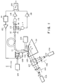
- Fig. 1 is a block diagram showing the constitution of the information processing device according to an example of the present invention.
- Fig. 1 as the recording medium 102, for example, built-up films of monomolecular film layer are formed according to the Langmuir-Blodgett method by use of 10,12-pentacosadiynic acid CH3(CH2)11C ⁇ C-C ⁇ C(CHC2)8COOH, amphiphilic diacetylene derivative, on the surface of an electroconductive prism 101 and a polymer is formed by irradiation of X-ray or gamma-ray.
- the material for the electroconductive prism 101 Ag2O-AgI-MoO3(P2O5) type super-ion conducting glass, a glass containing a polyvalent element such as palladium, iron, etc., or one coated on the glass surface with a thin film composed mainly of SnO2 may be employed.
- the light with wavelength ⁇ 1 generated from the light source 103 and the light with wavelength ⁇ 2 generated from the light source 104 are respectively passed through the beam expanders 105, 106 and the beam mixer 107 to be combined, and permitted to enter the surface of the recording medium 102 in contact with the electroconductive prism 101 under the total reflection condition.
- the electroconductive optical probe 109 is approximated to a distance of about sub-nanometer to the desired position of the recording medium 102.
- the electroconductive optical probe one prepared by polishing one end of the optical fiber made of the same material as the electroconductive prism 101 to have the tip end pointed (radius of curvature ⁇ 1 ⁇ m) is used.
- the evanescent light 100 having thus passed through the recording medium 102 to be oozed out (existing only in the vicinity of the surface) is detected by the electroconductive optical probe 109, introduced into the optical fiber 111, passed through the lens 112, the beam splitter 113, the filters 114, 115 to be divided into the components with wavelengths ⁇ 1 and ⁇ 2, which are respectively converted by photo-multipliers 116, 117 into electrical signals.
- the electrical signals are amplified in the amplifiers 118, 119 (I1, I2), then inputted in the dividing circuit 120 to make the ratio I2/I1 of the two signals the reproduction signal.
- the Z-directional position control of the optical probe 109 during recording and reproduction is performed as follows.
- the signal I1 for the detection light intensity of the wavelength ⁇ 1 is inputted in the feed-back circuit 121, the deviation from the set (light intensity) value is calculated, and after amplification in the amplification circuit 122, as the Z position control signal, by the xyz position control device 108, the Z-directional position of the optical probe 109 is controlled so as to become the set light intensity.
- the optical probe 109 is moved to the desired position of the recording medium 102, and a pulse voltage for recording is applied by the recording signal circuit 124 between the electroconductive optical probe 109 and the electroconductive prism 101 to inject locally electrons into the recording medium. Then, a structural change takes place in the diacetylene derivative polymer through the Joule's heat by the local current, whereby the peak of the absorption band of light is shifted from 640 nm to 580 nm.
- a material of which the absorption band of light can be shifted by electron injection or Joule's heat by current may be available, and otherwise, one decomposable by current Joule's heat such as J associated product of a dye such as squarilium bis-6 octylazulene, etc. (absorption band at wavelength 579 nm to be shifted to 890 nm), or one reduced as follows by electron injection such as polyimide: or one which is greatly changed in absorbance at around 800 nm by intramolecular charge transfer such as copper tetracyanoquinodimethane by electron injection as shown below: may be employed.
Landscapes
- Physics & Mathematics (AREA)
- Optics & Photonics (AREA)
- Optical Recording Or Reproduction (AREA)
- Indexing, Searching, Synchronizing, And The Amount Of Synchronization Travel Of Record Carriers (AREA)
- Optical Head (AREA)
- Signal Processing For Digital Recording And Reproducing (AREA)
- Recording Measured Values (AREA)
- Transition And Organic Metals Composition Catalysts For Addition Polymerization (AREA)
- Optical Record Carriers And Manufacture Thereof (AREA)
- Debugging And Monitoring (AREA)
Applications Claiming Priority (4)
| Application Number | Priority Date | Filing Date | Title |
|---|---|---|---|
| JP20661790 | 1990-08-03 | ||
| JP206617/90 | 1990-08-03 | ||
| JP2206617A JP2744339B2 (ja) | 1990-08-03 | 1990-08-03 | 情報処理装置及び情報処理方法 |
| EP91307007A EP0469879B1 (fr) | 1990-08-03 | 1991-07-31 | Dispositif et méthode d'enregistrement d'information |
Related Parent Applications (2)
| Application Number | Title | Priority Date | Filing Date |
|---|---|---|---|
| EP91307007.4 Division | 1991-07-31 | ||
| EP91307007A Division EP0469879B1 (fr) | 1990-08-03 | 1991-07-31 | Dispositif et méthode d'enregistrement d'information |
Publications (3)
| Publication Number | Publication Date |
|---|---|
| EP0676749A2 true EP0676749A2 (fr) | 1995-10-11 |
| EP0676749A3 EP0676749A3 (fr) | 1996-07-17 |
| EP0676749B1 EP0676749B1 (fr) | 2000-05-17 |
Family
ID=16526343
Family Applications (2)
| Application Number | Title | Priority Date | Filing Date |
|---|---|---|---|
| EP95201397A Expired - Lifetime EP0676749B1 (fr) | 1990-08-03 | 1991-07-31 | Dispositif et méthode de reproduction d'information |
| EP91307007A Expired - Lifetime EP0469879B1 (fr) | 1990-08-03 | 1991-07-31 | Dispositif et méthode d'enregistrement d'information |
Family Applications After (1)
| Application Number | Title | Priority Date | Filing Date |
|---|---|---|---|
| EP91307007A Expired - Lifetime EP0469879B1 (fr) | 1990-08-03 | 1991-07-31 | Dispositif et méthode d'enregistrement d'information |
Country Status (6)
| Country | Link |
|---|---|
| US (1) | US5343460A (fr) |
| EP (2) | EP0676749B1 (fr) |
| JP (1) | JP2744339B2 (fr) |
| AT (2) | ATE144346T1 (fr) |
| CA (1) | CA2048365C (fr) |
| DE (2) | DE69132212T2 (fr) |
Families Citing this family (47)
| Publication number | Priority date | Publication date | Assignee | Title |
|---|---|---|---|---|
| JP3074357B2 (ja) * | 1991-10-03 | 2000-08-07 | セイコーインスツルメンツ株式会社 | 微細表面観察装置 |
| EP0568753A1 (fr) * | 1992-05-07 | 1993-11-10 | International Business Machines Corporation | Unité de mémoire optique à grande densité de données et méthode d'enregistrement et de reproduction d'informations |
| JPH0696714A (ja) * | 1992-09-14 | 1994-04-08 | Hitachi Ltd | 表面加工装置および記録装置 |
| JPH06187675A (ja) * | 1992-09-25 | 1994-07-08 | Canon Inc | 情報処理装置、及びそれを用いる情報処理方法 |
| JP3135389B2 (ja) * | 1992-10-23 | 2001-02-13 | 松下電器産業株式会社 | 情報再生方法、情報記録再生方法、情報再生装置、記録媒体及び光ヘッド |
| ATE242519T1 (de) * | 1993-03-08 | 2003-06-15 | Canon Kk | Bildverarbeitungsvorrichtung und aufzeichnungs- /wiedergabegerät |
| FR2704349B1 (fr) * | 1993-04-21 | 1995-07-07 | Centre Nat Rech Scient | Sensibilisation d'une surface en emission photonique par microscopie a champ proche. |
| US5410151A (en) * | 1993-07-15 | 1995-04-25 | Sumitomo Electric Lightwave Corp. | Fiber optic probe and method of making same |
| EP0648049A1 (fr) * | 1993-10-08 | 1995-04-12 | Hitachi, Ltd. | Procédé et appareil d'enregistrement et reproduction d'information |
| US5513168A (en) * | 1993-10-19 | 1996-04-30 | Seiko Instruments Inc. | Optical information read/write apparatus |
| JPH087323A (ja) * | 1994-06-17 | 1996-01-12 | Hitachi Ltd | 光ヘッドおよび光情報記録再生装置 |
| US5751683A (en) | 1995-07-24 | 1998-05-12 | General Nanotechnology, L.L.C. | Nanometer scale data storage device and associated positioning system |
| US6339217B1 (en) * | 1995-07-28 | 2002-01-15 | General Nanotechnology Llc | Scanning probe microscope assembly and method for making spectrophotometric, near-field, and scanning probe measurements |
| US6337479B1 (en) | 1994-07-28 | 2002-01-08 | Victor B. Kley | Object inspection and/or modification system and method |
| JP2936311B2 (ja) * | 1994-09-09 | 1999-08-23 | セイコーインスツルメンツ株式会社 | 液中観察機能付き走査型近視野原子間力顕微鏡 |
| US6507553B2 (en) | 1995-07-24 | 2003-01-14 | General Nanotechnology Llc | Nanometer scale data storage device and associated positioning system |
| US5808973A (en) * | 1995-09-06 | 1998-09-15 | Kabushiki Kaisha Toshiba | Near field recording and reproducing apparatus |
| JP3622800B2 (ja) * | 1995-11-17 | 2005-02-23 | リコープリンティングシステムズ株式会社 | 光記録装置 |
| JP3618896B2 (ja) * | 1996-03-29 | 2005-02-09 | キヤノン株式会社 | 微小開口を有するプローブの作製法とそれによるプローブ、並びに該プローブを用いた走査型近接場光顕微鏡と走査型トンネル顕微鏡との複合装置、および該プローブを用いた記録再生装置 |
| US5689480A (en) * | 1996-08-13 | 1997-11-18 | The Board Of Trustees Of The Leland Stanford Junior University | Magneto-optic recording system employing near field optics |
| US5859814A (en) * | 1996-10-18 | 1999-01-12 | The Board Of Trustees Of The Leland Stanford Junior University | Magneto-optic recording system and method |
| JPH10293134A (ja) | 1997-02-19 | 1998-11-04 | Canon Inc | 光検出または照射用のプローブ、及び該プローブを備えた近視野光学顕微鏡・記録再生装置・露光装置、並びに該プローブの製造方法 |
| US6806477B1 (en) | 1997-05-23 | 2004-10-19 | Canon Kabushiki Kaisha | Position detection device, apparatus using the same, exposure apparatus, and device manufacturing method using the same |
| EP0880078A3 (fr) * | 1997-05-23 | 2001-02-14 | Canon Kabushiki Kaisha | Dispositif de détection de position, appareil l'utilisant, appareil d'exposition, et méthode de fabrication d'un dispositif l'utilisant |
| US5883872A (en) * | 1997-05-29 | 1999-03-16 | The Board Of Trustees Of The Leland Stanford Junior University | Near field magneto-optical recording system employing slit illumination |
| JP3524343B2 (ja) | 1997-08-26 | 2004-05-10 | キヤノン株式会社 | 微小開口の形成方法と微小開口を有する突起、及びそれらによるプローブまたはマルチプローブ、並びに該プローブを用いた表面観察装置、露光装置、情報処理装置 |
| JP3697034B2 (ja) * | 1997-08-26 | 2005-09-21 | キヤノン株式会社 | 微小開口を有する突起の製造方法、及びそれらによるプローブまたはマルチプローブ |
| JPH1183870A (ja) * | 1997-09-11 | 1999-03-26 | Canon Inc | 微細加工方法 |
| US6787768B1 (en) | 2001-03-08 | 2004-09-07 | General Nanotechnology Llc | Method and apparatus for tool and tip design for nanomachining and measurement |
| US6802646B1 (en) | 2001-04-30 | 2004-10-12 | General Nanotechnology Llc | Low-friction moving interfaces in micromachines and nanomachines |
| US6752008B1 (en) | 2001-03-08 | 2004-06-22 | General Nanotechnology Llc | Method and apparatus for scanning in scanning probe microscopy and presenting results |
| US7196328B1 (en) | 2001-03-08 | 2007-03-27 | General Nanotechnology Llc | Nanomachining method and apparatus |
| US6923044B1 (en) | 2001-03-08 | 2005-08-02 | General Nanotechnology Llc | Active cantilever for nanomachining and metrology |
| US6466537B1 (en) * | 1998-03-20 | 2002-10-15 | Seiko Instruments Inc. | Recording apparatus |
| JP2000036128A (ja) * | 1998-05-11 | 2000-02-02 | Seiko Instruments Inc | 近視野光学ヘッドおよび再生方法 |
| DE19822869C2 (de) * | 1998-05-22 | 2001-05-10 | Zeiss Carl Jena Gmbh | Optisches Nahfeldmikroskop |
| EP0959372A3 (fr) * | 1998-05-22 | 2000-07-19 | Rohm And Haas Company | Conduit de lumière |
| JP3901867B2 (ja) | 1999-02-08 | 2007-04-04 | 富士フイルム株式会社 | 近接場光記録再生装置 |
| AU6061100A (en) | 1999-07-01 | 2001-01-22 | General Nanotechnology, Llc | Object inspection and/or modification system and method |
| JP2002005810A (ja) | 2000-06-16 | 2002-01-09 | Canon Inc | プローブ及びその製造方法、表面観察装置、露光装置、情報処理装置 |
| US6931710B2 (en) * | 2001-01-30 | 2005-08-23 | General Nanotechnology Llc | Manufacturing of micro-objects such as miniature diamond tool tips |
| US7253407B1 (en) | 2001-03-08 | 2007-08-07 | General Nanotechnology Llc | Active cantilever for nanomachining and metrology |
| US7053369B1 (en) | 2001-10-19 | 2006-05-30 | Rave Llc | Scan data collection for better overall data accuracy |
| US6813937B2 (en) | 2001-11-28 | 2004-11-09 | General Nanotechnology Llc | Method and apparatus for micromachines, microstructures, nanomachines and nanostructures |
| JP2003202284A (ja) * | 2002-01-09 | 2003-07-18 | Hitachi Ltd | 走査プローブ顕微鏡およびこれを用いた試料観察方法およびデバイス製造方法 |
| WO2004023490A2 (fr) | 2002-09-09 | 2004-03-18 | General Nanotechnology Llc | Délivrance de fluide pour la microscopie à balayage par sonde |
| JP4646838B2 (ja) * | 2006-03-17 | 2011-03-09 | キヤノン株式会社 | プローブ及び近接場顕微鏡 |
Citations (3)
| Publication number | Priority date | Publication date | Assignee | Title |
|---|---|---|---|---|
| US4684206A (en) | 1982-12-27 | 1987-08-04 | International Business Machines Corporation | Light waveguide with a submicron aperture, method for manufacturing the waveguide and application of the waveguide in an optical memory |
| JPS63161553A (ja) | 1986-12-24 | 1988-07-05 | Canon Inc | 再生装置及び再生法 |
| JPS63161552A (ja) | 1986-12-24 | 1988-07-05 | Canon Inc | 記録装置及び記録法 |
Family Cites Families (20)
| Publication number | Priority date | Publication date | Assignee | Title |
|---|---|---|---|---|
| DE3276138D1 (en) * | 1982-12-27 | 1987-05-27 | Ibm | Optical near-field scanning microscope |
| US4662747A (en) * | 1983-08-03 | 1987-05-05 | Cornell Research Foundation, Inc. | Method and apparatus for production and use of nanometer scale light beams |
| US5055936A (en) * | 1986-12-30 | 1991-10-08 | Victor Company Of Japan, Ltd. | Charge latent image recording medium and recording/reproducing apparatus thereof |
| US4933926A (en) * | 1987-02-13 | 1990-06-12 | Fuji Photo Film Co., Ltd. | Image forming medium, method and apparatus |
| US5192631A (en) * | 1987-03-18 | 1993-03-09 | Dai Nippon Insatsu Kabushiki Kaisha | Variable electroconductivity material |
| EP0289642B1 (fr) * | 1987-05-08 | 1991-12-04 | International Business Machines Corporation | Disque de mémoire électro-optique effaçable |
| JPS63317936A (ja) * | 1987-06-19 | 1988-12-26 | Mitsubishi Electric Corp | 光学的波長多重記録再生装置 |
| EP0296262B1 (fr) * | 1987-06-22 | 1991-08-28 | International Business Machines Corporation | Procédé pour étudier des surfaces avec une résolution de l'ordre du nanomètre et de la picoseconde ainsi qu'un microscope à effet tunnel à balayage balayé au laser pour l'exécution du procédé |
| US4916688A (en) * | 1988-03-31 | 1990-04-10 | International Business Machines Corporation | Data storage method using state transformable materials |
| EP0355241A1 (fr) * | 1988-08-18 | 1990-02-28 | International Business Machines Corporation | Microscope à effet tunnel à polarisation de spin |
| US5191574A (en) * | 1988-08-25 | 1993-03-02 | Sparta Systems, Inc. | Optical memory method and apparatus utilizing frequency channeling and Stark effect |
| ATE139051T1 (de) * | 1988-10-04 | 1996-06-15 | Canon Kk | Gerät und verfahren zur aufzeichnung und wiedergabe und aufzeichnungsmedium für das aufzeichungs- und wiedergabeverfahren |
| US5018865A (en) * | 1988-10-21 | 1991-05-28 | Ferrell Thomas L | Photon scanning tunneling microscopy |
| US5091880A (en) * | 1989-02-02 | 1992-02-25 | Olympus Optical Co., Ltd. | Memory device |
| US5144581A (en) * | 1989-02-09 | 1992-09-01 | Olympus Optical Co., Ltd. | Apparatus including atomic probes utilizing tunnel current to read, write and erase data |
| JPH0354975A (ja) * | 1989-03-30 | 1991-03-08 | Victor Co Of Japan Ltd | 静電潜像記録素子及び/又は再生素子 |
| JP2846342B2 (ja) * | 1989-06-07 | 1999-01-13 | 株式会社日立製作所 | 高密度光再生装置 |
| US5179533A (en) * | 1989-07-31 | 1993-01-12 | Radiant Technologies | Read/write optical memory |
| US5161147A (en) * | 1989-08-30 | 1992-11-03 | Hoechst Celanese Corp. | High speed information system utilizing scanning tunneling microscopy in conjunction with a modulated light source |
| CA2021582A1 (fr) * | 1989-08-30 | 1991-03-01 | Harris A. Goldberg | Microscope a effet tunnel pour la lecture optique d'un support fluorescent |
-
1990
- 1990-08-03 JP JP2206617A patent/JP2744339B2/ja not_active Expired - Fee Related
-
1991
- 1991-07-31 AT AT91307007T patent/ATE144346T1/de not_active IP Right Cessation
- 1991-07-31 DE DE69132212T patent/DE69132212T2/de not_active Expired - Fee Related
- 1991-07-31 US US07/738,427 patent/US5343460A/en not_active Expired - Fee Related
- 1991-07-31 DE DE69122695T patent/DE69122695T2/de not_active Expired - Fee Related
- 1991-07-31 AT AT95201397T patent/ATE193142T1/de not_active IP Right Cessation
- 1991-07-31 EP EP95201397A patent/EP0676749B1/fr not_active Expired - Lifetime
- 1991-07-31 EP EP91307007A patent/EP0469879B1/fr not_active Expired - Lifetime
- 1991-08-02 CA CA002048365A patent/CA2048365C/fr not_active Expired - Fee Related
Patent Citations (3)
| Publication number | Priority date | Publication date | Assignee | Title |
|---|---|---|---|---|
| US4684206A (en) | 1982-12-27 | 1987-08-04 | International Business Machines Corporation | Light waveguide with a submicron aperture, method for manufacturing the waveguide and application of the waveguide in an optical memory |
| JPS63161553A (ja) | 1986-12-24 | 1988-07-05 | Canon Inc | 再生装置及び再生法 |
| JPS63161552A (ja) | 1986-12-24 | 1988-07-05 | Canon Inc | 記録装置及び記録法 |
Non-Patent Citations (3)
| Title |
|---|
| DUERIG ET AL., J. APPL. PHYS., vol. 59, 1986, pages 3318 |
| G. BINNIG ET AL., PHYS. REV. LETT., vol. 49, 1982, pages 57 |
| REDDICK ET AL., PHYS. REV., vol. B39, 1989, pages 767 |
Also Published As
| Publication number | Publication date |
|---|---|
| DE69122695D1 (de) | 1996-11-21 |
| JP2744339B2 (ja) | 1998-04-28 |
| US5343460A (en) | 1994-08-30 |
| EP0469879B1 (fr) | 1996-10-16 |
| EP0676749B1 (fr) | 2000-05-17 |
| JPH0490152A (ja) | 1992-03-24 |
| EP0676749A3 (fr) | 1996-07-17 |
| CA2048365C (fr) | 1996-12-31 |
| DE69132212D1 (de) | 2000-06-21 |
| CA2048365A1 (fr) | 1992-02-04 |
| DE69122695T2 (de) | 1997-02-27 |
| DE69132212T2 (de) | 2000-10-26 |
| EP0469879A3 (en) | 1992-06-03 |
| EP0469879A2 (fr) | 1992-02-05 |
| ATE193142T1 (de) | 2000-06-15 |
| ATE144346T1 (de) | 1996-11-15 |
Similar Documents
| Publication | Publication Date | Title |
|---|---|---|
| EP0676749B1 (fr) | Dispositif et méthode de reproduction d'information | |
| US5389475A (en) | Recording medium and information-erasing method | |
| EP0381158B1 (fr) | Dispositif de mémoire | |
| EP0363147B1 (fr) | Appareil et procédé d'enregistrement et de reproduction et milieu d'enregistrement pour le procédé d'enregistrement et de reproduction | |
| JPH04339337A (ja) | 情報処理装置 | |
| JPH0696714A (ja) | 表面加工装置および記録装置 | |
| US5325342A (en) | Surface-enhanced raman optical data storage system | |
| JP3029143B2 (ja) | 情報再生方法 | |
| JPH0298849A (ja) | 記録・再生装置及び該装置を用いた記録・再生方法 | |
| JP2000036139A (ja) | 表面観察方法及び記録再生方法、並びに、走査型プローブ顕微鏡及び記録再生装置 | |
| JP3236423B2 (ja) | 光メモリ装置並びにその記録方法及び再生方法 | |
| JP3044421B2 (ja) | 記録媒体製造方法 | |
| JP2872662B2 (ja) | 記録媒体及びその消去方法 | |
| JP3005077B2 (ja) | 記録及び/又は再生方法及び装置 | |
| JP2859719B2 (ja) | 記録・消去方法、及び記録・消去装置、記録・再生・消去装置 | |
| JP3086988B2 (ja) | 情報処理装置 | |
| JPH02146128A (ja) | 記録再生装置 | |
| JP2994833B2 (ja) | 記録及び/又は再生装置、方法と情報検出装置 | |
| JPH06295477A (ja) | 情報処理装置 | |
| JP2962603B2 (ja) | 情報記録方法 | |
| JP2942011B2 (ja) | 情報記憶装置 | |
| JP2992908B2 (ja) | 基板電極の製造方法、記録媒体の製造方法 | |
| JPH0316046A (ja) | 記録及び再生装置 | |
| JPH07191046A (ja) | 光ファイバプローブ記録及び観察装置 | |
| JPH04123338A (ja) | 情報再生装置および方法 |
Legal Events
| Date | Code | Title | Description |
|---|---|---|---|
| PUAI | Public reference made under article 153(3) epc to a published international application that has entered the european phase |
Free format text: ORIGINAL CODE: 0009012 |
|
| AC | Divisional application: reference to earlier application |
Ref document number: 469879 Country of ref document: EP |
|
| AK | Designated contracting states |
Kind code of ref document: A2 Designated state(s): AT BE CH DE DK ES FR GB GR IT LI LU NL SE |
|
| PUAL | Search report despatched |
Free format text: ORIGINAL CODE: 0009013 |
|
| AK | Designated contracting states |
Kind code of ref document: A3 Designated state(s): AT BE CH DE DK ES FR GB GR IT LI LU NL SE |
|
| 17P | Request for examination filed |
Effective date: 19961128 |
|
| 17Q | First examination report despatched |
Effective date: 19981125 |
|
| GRAG | Despatch of communication of intention to grant |
Free format text: ORIGINAL CODE: EPIDOS AGRA |
|
| GRAG | Despatch of communication of intention to grant |
Free format text: ORIGINAL CODE: EPIDOS AGRA |
|
| GRAH | Despatch of communication of intention to grant a patent |
Free format text: ORIGINAL CODE: EPIDOS IGRA |
|
| GRAH | Despatch of communication of intention to grant a patent |
Free format text: ORIGINAL CODE: EPIDOS IGRA |
|
| GRAA | (expected) grant |
Free format text: ORIGINAL CODE: 0009210 |
|
| AC | Divisional application: reference to earlier application |
Ref document number: 469879 Country of ref document: EP |
|
| AK | Designated contracting states |
Kind code of ref document: B1 Designated state(s): AT BE CH DE DK ES FR GB GR IT LI LU NL SE |
|
| PG25 | Lapsed in a contracting state [announced via postgrant information from national office to epo] |
Ref country code: NL Free format text: LAPSE BECAUSE OF FAILURE TO SUBMIT A TRANSLATION OF THE DESCRIPTION OR TO PAY THE FEE WITHIN THE PRESCRIBED TIME-LIMIT Effective date: 20000517 Ref country code: LI Free format text: LAPSE BECAUSE OF FAILURE TO SUBMIT A TRANSLATION OF THE DESCRIPTION OR TO PAY THE FEE WITHIN THE PRESCRIBED TIME-LIMIT Effective date: 20000517 Ref country code: GR Free format text: LAPSE BECAUSE OF NON-PAYMENT OF DUE FEES Effective date: 20000517 Ref country code: ES Free format text: THE PATENT HAS BEEN ANNULLED BY A DECISION OF A NATIONAL AUTHORITY Effective date: 20000517 Ref country code: CH Free format text: LAPSE BECAUSE OF FAILURE TO SUBMIT A TRANSLATION OF THE DESCRIPTION OR TO PAY THE FEE WITHIN THE PRESCRIBED TIME-LIMIT Effective date: 20000517 Ref country code: BE Free format text: LAPSE BECAUSE OF FAILURE TO SUBMIT A TRANSLATION OF THE DESCRIPTION OR TO PAY THE FEE WITHIN THE PRESCRIBED TIME-LIMIT Effective date: 20000517 Ref country code: AT Free format text: LAPSE BECAUSE OF FAILURE TO SUBMIT A TRANSLATION OF THE DESCRIPTION OR TO PAY THE FEE WITHIN THE PRESCRIBED TIME-LIMIT Effective date: 20000517 |
|
| REF | Corresponds to: |
Ref document number: 193142 Country of ref document: AT Date of ref document: 20000615 Kind code of ref document: T |
|
| REG | Reference to a national code |
Ref country code: CH Ref legal event code: EP |
|
| REF | Corresponds to: |
Ref document number: 69132212 Country of ref document: DE Date of ref document: 20000621 |
|
| ET | Fr: translation filed | ||
| ITF | It: translation for a ep patent filed | ||
| PG25 | Lapsed in a contracting state [announced via postgrant information from national office to epo] |
Ref country code: LU Free format text: LAPSE BECAUSE OF NON-PAYMENT OF DUE FEES Effective date: 20000731 |
|
| PG25 | Lapsed in a contracting state [announced via postgrant information from national office to epo] |
Ref country code: SE Free format text: LAPSE BECAUSE OF FAILURE TO SUBMIT A TRANSLATION OF THE DESCRIPTION OR TO PAY THE FEE WITHIN THE PRESCRIBED TIME-LIMIT Effective date: 20000817 Ref country code: DK Free format text: LAPSE BECAUSE OF FAILURE TO SUBMIT A TRANSLATION OF THE DESCRIPTION OR TO PAY THE FEE WITHIN THE PRESCRIBED TIME-LIMIT Effective date: 20000817 |
|
| NLV1 | Nl: lapsed or annulled due to failure to fulfill the requirements of art. 29p and 29m of the patents act | ||
| REG | Reference to a national code |
Ref country code: CH Ref legal event code: PL |
|
| PLBE | No opposition filed within time limit |
Free format text: ORIGINAL CODE: 0009261 |
|
| STAA | Information on the status of an ep patent application or granted ep patent |
Free format text: STATUS: NO OPPOSITION FILED WITHIN TIME LIMIT |
|
| 26N | No opposition filed | ||
| REG | Reference to a national code |
Ref country code: GB Ref legal event code: IF02 |
|
| PGFP | Annual fee paid to national office [announced via postgrant information from national office to epo] |
Ref country code: FR Payment date: 20040716 Year of fee payment: 14 |
|
| PGFP | Annual fee paid to national office [announced via postgrant information from national office to epo] |
Ref country code: GB Payment date: 20040719 Year of fee payment: 14 |
|
| PGFP | Annual fee paid to national office [announced via postgrant information from national office to epo] |
Ref country code: DE Payment date: 20040922 Year of fee payment: 14 |
|
| PG25 | Lapsed in a contracting state [announced via postgrant information from national office to epo] |
Ref country code: IT Free format text: LAPSE BECAUSE OF NON-PAYMENT OF DUE FEES Effective date: 20050731 Ref country code: GB Free format text: LAPSE BECAUSE OF NON-PAYMENT OF DUE FEES Effective date: 20050731 |
|
| PG25 | Lapsed in a contracting state [announced via postgrant information from national office to epo] |
Ref country code: DE Free format text: LAPSE BECAUSE OF NON-PAYMENT OF DUE FEES Effective date: 20060201 |
|
| GBPC | Gb: european patent ceased through non-payment of renewal fee |
Effective date: 20050731 |
|
| PG25 | Lapsed in a contracting state [announced via postgrant information from national office to epo] |
Ref country code: FR Free format text: LAPSE BECAUSE OF NON-PAYMENT OF DUE FEES Effective date: 20060331 |
|
| REG | Reference to a national code |
Ref country code: FR Ref legal event code: ST Effective date: 20060331 |