EP0676873A2 - Dispositif pour la récupération d'un signal numérique plésiochrone - Google Patents
Dispositif pour la récupération d'un signal numérique plésiochrone Download PDFInfo
- Publication number
- EP0676873A2 EP0676873A2 EP95104589A EP95104589A EP0676873A2 EP 0676873 A2 EP0676873 A2 EP 0676873A2 EP 95104589 A EP95104589 A EP 95104589A EP 95104589 A EP95104589 A EP 95104589A EP 0676873 A2 EP0676873 A2 EP 0676873A2
- Authority
- EP
- European Patent Office
- Prior art keywords
- divider
- arrangement according
- ramp generator
- clock
- frequency
- Prior art date
- Legal status (The legal status is an assumption and is not a legal conclusion. Google has not performed a legal analysis and makes no representation as to the accuracy of the status listed.)
- Ceased
Links
- 238000012937 correction Methods 0.000 claims abstract description 39
- 230000015654 memory Effects 0.000 claims abstract description 24
- 238000000034 method Methods 0.000 claims description 16
- 230000001419 dependent effect Effects 0.000 claims description 5
- 230000001360 synchronised effect Effects 0.000 claims description 4
- 230000006870 function Effects 0.000 claims description 3
- 230000005540 biological transmission Effects 0.000 description 5
- 238000001514 detection method Methods 0.000 description 4
- 238000010586 diagram Methods 0.000 description 4
- 238000005562 fading Methods 0.000 description 4
- 238000003780 insertion Methods 0.000 description 2
- 230000037431 insertion Effects 0.000 description 2
- 102100029469 WD repeat and HMG-box DNA-binding protein 1 Human genes 0.000 description 1
- 101710097421 WD repeat and HMG-box DNA-binding protein 1 Proteins 0.000 description 1
- 230000006978 adaptation Effects 0.000 description 1
- 230000015572 biosynthetic process Effects 0.000 description 1
- 230000007423 decrease Effects 0.000 description 1
- 230000000694 effects Effects 0.000 description 1
- 238000005516 engineering process Methods 0.000 description 1
- 238000010606 normalization Methods 0.000 description 1
- 238000001208 nuclear magnetic resonance pulse sequence Methods 0.000 description 1
- 230000010363 phase shift Effects 0.000 description 1
- 238000011084 recovery Methods 0.000 description 1
- 238000003786 synthesis reaction Methods 0.000 description 1
Images

Classifications
-
- H—ELECTRICITY
- H04—ELECTRIC COMMUNICATION TECHNIQUE
- H04J—MULTIPLEX COMMUNICATION
- H04J3/00—Time-division multiplex systems
- H04J3/02—Details
- H04J3/06—Synchronising arrangements
- H04J3/07—Synchronising arrangements using pulse stuffing for systems with different or fluctuating information rates or bit rates
- H04J3/076—Bit and byte stuffing, e.g. SDH/PDH desynchronisers, bit-leaking
Definitions
- the invention relates to an arrangement for recovering a plesiochronous digital signal
- bit rates are adjusted by stuffing.
- the transmitted signal contains the data signal and, at regular intervals, justification points, which contain either bits of the data signal or empty bits as required. If the bit rate of the data signal remains behind the reserved transmission bit rate, empty bits must be inserted; this is called positive plug.
- the bit rate of the data signal exceeds the reserved transmission bit rate, then at least one data bit is additionally inserted into the justification point (s); this is called a negative plug.
- Tamping processes that use both types of tamping are referred to as positive-zero-negative tamping processes. These processes are applied even when multiple digital signals are combined into a multiplex signal, or if multiplex signals are combined a lower hierarchy level to a multiplex signal of a higher hierarchical level, as for example in the usual PCM multiplexing method or the s ynchronen d igitalen H ierarchie (SDH ) he follows.
- the stuffing operations each include one bit or more bits or one or more bytes.
- Each tamping process creates a phase jump in the outgoing digital signal.
- the digital signal is on the receiving side written into a buffer memory with a gap clock signal and read out with a continuous clock signal.
- the phase jumps of the digital signal or the associated output clock signal are smoothed at the receiving location by an analog or digital phase locked loop (PLL).
- PLL phase locked loop
- the phase-locked loop acts like a low-pass filter.
- the amplitude of the phase jumps (jitter) caused by plugging is greatly reduced by the phase-locked loop if the time interval between the phase jumps is very small compared to the time constant of the phase-locked loop.
- phase jumps With the positive-zero-negative stuffing method, the time intervals of the phase jumps can be very large. In this case, the phase jumps are damped little by the phase locked loop without additional measures.
- a method and an arrangement for clock recovery are known from international patent application WO 91/12678. Abrupt changes in the correction variable for the control loop are initially suppressed, in order to then pass them on continuously or in small steps to a digitally executed phase control loop within a longer compensation time.
- the phase locked loop is controlled depending on the fill level of a ramp counter, in which the initial values are loaded during tamping processes. Only in the end position of the ramp counter is a PLL counter, which determines the frequency of the output clock, controlled by the fill level of the buffer memory.
- the control loop is designed in such a way that a phase correction is carried out continuously even with a synchronous clock signal. Numerous counters and a relatively complicated arithmetic are required for implementation. As a result, there is only a slow change in the phase of the clock signal.
- the object of the invention is to provide a simpler digitally working arrangement for the receiving part, which generates only a minimal jitter with a high frequency. It should be easy to adapt to the different data rates.
- This object is achieved by the arrangement for recovering a digital signal.
- phase correction is controlled only by the stuffing information and is not made dependent on the memory content as before.
- the fill level of the memory is also used as a control criterion for phase correction only in the switch-on phase and in the event of faults.
- An auxiliary oscillator is not required with this arrangement.
- the speed of the phase correction can also depend on the size and the frequency of the required phase correction specified by the stuffing information.
- One of the greatest advantages of the invention is the use of programmable dividers. This is the arrangement adaptable to the most varied data rates and to all requirements for the tamping processes.
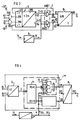
- the basic circuit diagram shown in FIG. 1 contains a clock regenerator 2, to which a synchronous multiplex signal MS is fed via input 1.
- the output of the clock regenerator is connected to a 'frame detection and clock supply' 3 which supplies the gap clocks TL1 to TLN assigned to the individual digital signals and the corresponding stuffing information SI1 to SIN.
- Circuits for a clock regenerator 2 and a 'frame recognition and clock supply' 3 are familiar to any person skilled in the art and are described, for example, in "Digital Transmission Technology" by Peter Kahl, Decker's Verlag, Volume 1 under 2.1.2.3.10, pages 22 to 25.
- the received multiplex signal MS is fed to the data inputs, for example the data input 61, from N buffer memories, of which only the buffer memory 6 is shown for the first data signal DS1.
- the stuffing information signals SI1 to SIN are each fed to a ramp counter 5 via an encoder 4. Its outputs 53 and 54 are via a logic circuit 7 with the control inputs 81 and 82 of a frequency divider 8 connected, the clock input E8 of the system clock TS is supplied.
- the clock output 11 of the frequency divider 8 is connected to the read clock input 64 of the buffer memory 6.
- a timer 9 supplies a memory clock signal TE derived from the system clock TS to the logic circuit 7.
- the buffer memory 6, the ramp counter 5 and the frequency divider 8 are provided separately for each digital signal.
- the encoder 4 and the timer 9 (or parts thereof) can be used in common for all digital signals.
- the system clock TS is derived in the clock regenerator 2 from the multiplex signal MS present at the input 1.
- the 'frame detection and clock supply' 3 recognizes the beginning of the frame by means of a frame password or corresponding defined bit sequences and assigns the individual digital signals, e.g. to the digital signal DS1, a corresponding gap clock, the write clock TL1, with which the digital signal DS1 is written into the buffer memory 6.
- the task of the ramp counter 5, the timer 9 and the frequency divider 8 is to generate an output clock TA1 which is as uniform as possible, with which the digital signal TS1 is read out from the buffer memory 6 and is output at the data output 62 of the memory or at the digital signal output 10, while the associated clock signal TA1 is present at the clock output 11.
- the data rate of the digital signal received and the digital signal read out must match.
- the output clock signal TA1 is not controlled by the filling level of the buffer memory but only by the stuffing information SI1 (if one disregards interference on the transmission path and the switch-on phase).
- the frequency divider 8 allows the aperiodic quasi-periodic frequency synthesis or frequency division, as described in the magazine Frequency 27, (1973) 9, pages 249 to 254 and Frequency 27 (1973) 10, pages 279 to 283. It consists of a first switchable A / B divider 86, the clock input E8 of which is supplied with the system clock signal TS and which outputs the output clock signal TA1 at the clock output 11.
- This divider is followed by a further C divider 87 which counts the subperiods and whose counter reading ZC specifies the current subperiod - A or B - of the A / B divider 86 and control signals SAP and SEP for determining the next subperiod via a decoder 88.
- the outputs of the decoder are routed to synchronization inputs 83 and 84 of a synchronization circuit 89. This is fed via the control inputs 81 and 82 phase correction commands EB and AB.
- the control output A89 leads to the control input of the C-divider 87.
- the frequency of the system clock is 129.6 MHz and the clock frequency of the output clock TA is 2.048 MHz.
- a suitable subperiod distribution for this is: BAAA BAA BAAA BAA BAAA BAA BAAA BAA BAAA BAA BAAA BAAA BAAA BAAA After each sub-period A or B, a pulse of the output clock signal TA1 is output, with which the digital signal DS1 is read out. These pulses of the output clock signal and the steps (bits) of the digital signal have a minimal jitter due to the frequency division, which need not be further reduced.
- a sub-period A or B is faded in or out via the synchronizing circuit by means of the synchronizing signal SY which intervenes in the C-divider.
- the fading in or out of a sub-period can take place at the same time intervals defined by the timer 9, which correspond to a normal over-period with 32 sub-periods. If this happens to be an unsuitable B sub-period, the next A sub-period is shown or hidden.
- the timer 9 can also be replaced by the dividers 86, 87 and the decoder 88.
- a modified store-in clock signal TEC is generated, the clocks of which have slightly different distances when fading in and out, but always occur at the same position of an overperiod - as in the following example - and via the dashed connection from the decoder to the synchronization circuit 89.
- a correction step should be carried out in every line. This is explained in more detail in the following Table 1. For example, a short A sub-period should be shown; this is sub-period A.
- the first line a00) shows the regular over-period of the frequency divider 8.
- an A sub-period z. B. in the sixth position there is an extended over-period a01), which has a short A-sub-period more, ie the average duration of the sub-period decreases slightly.
- the period pattern shifts to the right after each insertion of an A subperiod from the inserted A subperiod.
- the next line b01) in the table shows only the 32 sub-periods that belong to one over-period.
- the last A sub-period identified by a preceding space becomes the first sub-period of the next over-period b02) with 32 sub-periods.
- Some of the resulting over-periods are shown in Table 1, based on the original time frame.
- the original over-period is restored.
- a total of 9 B subperiods were replaced by 9 A subperiods and as a result the phase was corrected by 9 periods of the system clock signal (overperiod b00) without correction counted in).
- N 225 of these A sub-periods must be faded in in order to achieve a phase correction by one UI overall.
- the circuits for the A / B divider 86, the C divider 87 and the decoder 88 can be implemented in various ways by a person skilled in the art. It is also sufficient to feed back a line for controlling the A or B period if the correct times for switching between the periods are realized in the A / B divider 86 itself.
- Periods are faded in and faded out via control inputs 81 and 82.
- An 'insert command' EB causes a further A period to be faded in at a suitable point determined by decoder 88 and synchronization circuit 89 by fading out one of C divider 87 supplied clock (or a switchover of the period) by a corresponding synchronization command SY.
- a 'hide command' AB causes an additional pulse so that the C counter reaches its end position faster, so it only requires C-1 counting cycles.
- FIG. 1 An exemplary embodiment of the ramp generator 5 is shown in FIG.
- This contains a logic unit LE5, which may include the encoder 4, and an up-down counter VR5 with a counting range of +/- Zm.
- the logic unit LE5 is used to set the up-down counter VR5, at its output 53 a counter reading> 0 and at its output 54 a counter reading ⁇ 0.
- the frequency divider 8 is controlled, ie an A period (or B period) is faded in at the times at which a memory pulse TE is emitted by the timer 9 or is hidden.
- the function description is based on the counter reading zero of the up-down counter VR5, i.e. the frequency divider 8 works with its target division ratio (in the example 2025/32).
- the insert command EB is fed back via the logic unit LE 5 and causes the up-down counter to be counted down by 1. This process is repeated 224 more times until the numerical value corresponding to the phase shift of 1 bit has been processed and the zero position has been reached again .
- the numerical value 225 is added to the current counter reading in the logic unit LE5.
- a corresponding negative numerical value - N is entered into the counter and added to the counter reading and - in this example - a correspondingly large number of A periods are faded out, which have an effect on the output 85 of the frequency divider 8 as minimal negative phase jumps .
- a first OR gate OR1 can be used, or if the memory is empty, a second OR gate OR2 can be used by appropriate phase correction signals + SF and -SF, ie by entering a numerical value or several numerical values, an additional phase correction of the output clock TA and thus a normalization of the degree of filling.
- Some systems work with a variable number of stuff bits or stuff bytes. This only means that the input number value N is increased accordingly if more than one bit has to be corrected. If a new stuffing command is pending before the old stuffing command has been processed, the new numerical value N (or -N) to be stored is added or subtracted to the counter reading Z and the counter is loaded again with the result.
- This control loop always works with the correction speed specified by the timer 9.
- this can also be made variable by making the period of the store cycle TE dependent on the size of the stuffing criterion. Numerous circuit variants are again conceivable for this.
- FIG. 4 shows one possibility for realizing different phase correction speeds.
- the logic circuit 7 * connected between the ramp generator 5 and the frequency divider 8 contains a so-called segment 71, at whose outputs two distributor circuits 72 and 73 are connected.
- the timer 9 * delivers four different pulse sequences with the same phase spacing.
- the segment 71 now switches through one, two or four store cycles TE1 ... TE4 during a period of the timer 9 *, as a result of which the fade-in or fade-out during a period Sub-periods are possible several times.
- memory pulses with a correspondingly higher pulse repetition frequency (this corresponds to the combination of the pulses TE1 to TE4 via an OR circuit) are transmitted to the individual distributor circuits and the pulse trains are generated with frequency pulse frequencies that are sometimes lower by frequency dividers.
- the segment 71 can also be part of the synchronization circuit 89 in FIG. 2, to which the counter reading Z of the ramp counter is then also supplied via a further control input E89.
Landscapes
- Engineering & Computer Science (AREA)
- Computer Networks & Wireless Communication (AREA)
- Signal Processing (AREA)
- Synchronisation In Digital Transmission Systems (AREA)
- Stabilization Of Oscillater, Synchronisation, Frequency Synthesizers (AREA)
Applications Claiming Priority (2)
| Application Number | Priority Date | Filing Date | Title |
|---|---|---|---|
| DE19944412060 DE4412060C1 (de) | 1994-04-07 | 1994-04-07 | Anordnung zur Rückgewinnung eines plesiochronen Digitalsignals |
| DE4412060 | 1994-04-07 |
Publications (2)
| Publication Number | Publication Date |
|---|---|
| EP0676873A2 true EP0676873A2 (fr) | 1995-10-11 |
| EP0676873A3 EP0676873A3 (fr) | 1997-01-08 |
Family
ID=6514871
Family Applications (1)
| Application Number | Title | Priority Date | Filing Date |
|---|---|---|---|
| EP95104589A Ceased EP0676873A3 (fr) | 1994-04-07 | 1995-03-28 | Dispositif pour la récupération d'un signal numérique plésiochrone. |
Country Status (4)
| Country | Link |
|---|---|
| EP (1) | EP0676873A3 (fr) |
| AU (1) | AU669315B2 (fr) |
| DE (1) | DE4412060C1 (fr) |
| TW (1) | TW280971B (fr) |
Family Cites Families (5)
| Publication number | Priority date | Publication date | Assignee | Title |
|---|---|---|---|---|
| US5033064A (en) * | 1988-12-09 | 1991-07-16 | Transwitch Corporation | Clock dejitter circuit for regenerating DS1 signal |
| DE3934248A1 (de) * | 1989-10-13 | 1991-04-18 | Standard Elektrik Lorenz Ag | Multiplexer und demultiplexer, insbesondere fuer nachrichtenuebertragungs-netze mit einer synchronen hierarchie der digitalsignale |
| DE59006856D1 (de) * | 1990-02-16 | 1994-09-22 | Siemens Ag | Verfahren und anordnung zur taktrückgewinnung. |
| DE4035438A1 (de) * | 1990-11-08 | 1992-05-14 | Philips Patentverwaltung | Schaltungsanordnung zum entfernen von stopfbits |
| US5268935A (en) * | 1991-12-20 | 1993-12-07 | At&T Bell Laboratories | Synchronous digital signal to asynchronous digital signal desynchronizer |
-
1994
- 1994-04-07 DE DE19944412060 patent/DE4412060C1/de not_active Expired - Fee Related
-
1995
- 1995-03-28 EP EP95104589A patent/EP0676873A3/fr not_active Ceased
- 1995-04-06 AU AU16309/95A patent/AU669315B2/en not_active Ceased
- 1995-04-07 TW TW84103296A patent/TW280971B/zh active
Also Published As
| Publication number | Publication date |
|---|---|
| EP0676873A3 (fr) | 1997-01-08 |
| AU669315B2 (en) | 1996-05-30 |
| TW280971B (fr) | 1996-07-11 |
| AU1630995A (en) | 1995-11-16 |
| DE4412060C1 (de) | 1995-02-23 |
Similar Documents
| Publication | Publication Date | Title |
|---|---|---|
| DE69221101T2 (de) | Desynchronisierer von synchronen digitalen Signalen zu asynchronen digitalen Signalen | |
| EP0507385B1 (fr) | Système de transmission pour la hiérarchie numérique synchrone | |
| DE3151207C2 (de) | Speicheranordnung für eine PCM-Fernmeldevermittlungsanlage | |
| EP0429888B1 (fr) | Méthode de transmission par un réseau multiplex hierarchisé synchrone et numérique d'un signal à large bande distribué entre des unités de transmission subordonnées | |
| DE69123785T2 (de) | Synchronisierung eines digitalen Signals mit einer elastischen Speicherung | |
| DE69327479T2 (de) | Verfahren zum zerlegen und zusammensetzen von rahmenstrukturen mit zeigern | |
| EP0503732B1 (fr) | Méthode et système de transmission pour la hiérarchie numérique synchrone | |
| DE69104721T2 (de) | Verfahren und anordnung für datensynchronisierung. | |
| DE69330492T2 (de) | Desynchronisierer und verfahren zur unterdrückung des zeigerzitterns in einen desynchronisierer | |
| DE69034026T2 (de) | Taktjitter-Korrekturschaltungen zur Regenerierung von Taktsignalen mit Jitter | |
| DE69217526T2 (de) | Linearer In-line-Desynchronisierer | |
| EP0475498B1 (fr) | Circuit d'adaption du débit binaire de deux signaux numériques | |
| DE69132247T2 (de) | Phasenverriegelte Schleifenanordnung | |
| EP0639903A2 (fr) | Système de transmission | |
| EP0435383B1 (fr) | Circuit d'adaptation de débit binaire | |
| DE69323071T2 (de) | Anordnung von digitalen Phasenregelschleifen | |
| DE3215783C2 (de) | Digitale Datenübertragungsanlage mit störungsfreiem Umschalten von regulären Kanälen auf einen Reservekanal | |
| EP0708541A1 (fr) | Système de transmission avec une boucle de commande | |
| DE69321178T2 (de) | Phasendetektor für elastischen Speicherung | |
| DE69229668T2 (de) | Synchrone Schaltung | |
| DE69220267T2 (de) | Pulsstopfanlage | |
| EP0567517B1 (fr) | Procede et dispositif pour transmettre des signaux numeriques | |
| DE69320257T2 (de) | Verfahren und Anordnung zum Einschreiben und Auslesen in einem Speicher | |
| DE2908366C2 (de) | Verfahren und Schaltungsanordnung zur Reduzierung von Phasenschwankungen bei der Taktrückgewinnung in einem digitalen, hierarchisch gegliederten, plesiochronen Nachrichtenübertragungssystem | |
| DE19820658C2 (de) | Digitale Phasenregelschleife für Niedriggeschwindigkeitssignalschaltsystem mit plesiochroner digitaler Hierarchie |
Legal Events
| Date | Code | Title | Description |
|---|---|---|---|
| PUAI | Public reference made under article 153(3) epc to a published international application that has entered the european phase |
Free format text: ORIGINAL CODE: 0009012 |
|
| AK | Designated contracting states |
Kind code of ref document: A2 Designated state(s): DE FR GB IT |
|
| PUAL | Search report despatched |
Free format text: ORIGINAL CODE: 0009013 |
|
| AK | Designated contracting states |
Kind code of ref document: A3 Designated state(s): DE FR GB IT |
|
| 17P | Request for examination filed |
Effective date: 19970206 |
|
| 17Q | First examination report despatched |
Effective date: 20010807 |
|
| GRAG | Despatch of communication of intention to grant |
Free format text: ORIGINAL CODE: EPIDOS AGRA |
|
| STAA | Information on the status of an ep patent application or granted ep patent |
Free format text: STATUS: THE APPLICATION HAS BEEN REFUSED |
|
| 18R | Application refused |
Effective date: 20020831 |