EP0677765B1 - Dispositif optique à guide d'onde - Google Patents
Dispositif optique à guide d'onde Download PDFInfo
- Publication number
- EP0677765B1 EP0677765B1 EP95108382A EP95108382A EP0677765B1 EP 0677765 B1 EP0677765 B1 EP 0677765B1 EP 95108382 A EP95108382 A EP 95108382A EP 95108382 A EP95108382 A EP 95108382A EP 0677765 B1 EP0677765 B1 EP 0677765B1
- Authority
- EP
- European Patent Office
- Prior art keywords
- optical waveguide
- electrodes
- semiconductive layer
- pair
- layer
- Prior art date
- Legal status (The legal status is an assumption and is not a legal conclusion. Google has not performed a legal analysis and makes no representation as to the accuracy of the status listed.)
- Expired - Lifetime
Links
Images


Classifications
-
- G—PHYSICS
- G02—OPTICS
- G02F—OPTICAL DEVICES OR ARRANGEMENTS FOR THE CONTROL OF LIGHT BY MODIFICATION OF THE OPTICAL PROPERTIES OF THE MEDIA OF THE ELEMENTS INVOLVED THEREIN; NON-LINEAR OPTICS; FREQUENCY-CHANGING OF LIGHT; OPTICAL LOGIC ELEMENTS; OPTICAL ANALOGUE/DIGITAL CONVERTERS
- G02F1/00—Devices or arrangements for the control of the intensity, colour, phase, polarisation or direction of light arriving from an independent light source, e.g. switching, gating or modulating; Non-linear optics
- G02F1/01—Devices or arrangements for the control of the intensity, colour, phase, polarisation or direction of light arriving from an independent light source, e.g. switching, gating or modulating; Non-linear optics for the control of the intensity, phase, polarisation or colour
- G02F1/03—Devices or arrangements for the control of the intensity, colour, phase, polarisation or direction of light arriving from an independent light source, e.g. switching, gating or modulating; Non-linear optics for the control of the intensity, phase, polarisation or colour based on ceramics or electro-optical crystals, e.g. exhibiting Pockels effect or Kerr effect
- G02F1/035—Devices or arrangements for the control of the intensity, colour, phase, polarisation or direction of light arriving from an independent light source, e.g. switching, gating or modulating; Non-linear optics for the control of the intensity, phase, polarisation or colour based on ceramics or electro-optical crystals, e.g. exhibiting Pockels effect or Kerr effect in an optical waveguide structure
-
- G—PHYSICS
- G02—OPTICS
- G02F—OPTICAL DEVICES OR ARRANGEMENTS FOR THE CONTROL OF LIGHT BY MODIFICATION OF THE OPTICAL PROPERTIES OF THE MEDIA OF THE ELEMENTS INVOLVED THEREIN; NON-LINEAR OPTICS; FREQUENCY-CHANGING OF LIGHT; OPTICAL LOGIC ELEMENTS; OPTICAL ANALOGUE/DIGITAL CONVERTERS
- G02F1/00—Devices or arrangements for the control of the intensity, colour, phase, polarisation or direction of light arriving from an independent light source, e.g. switching, gating or modulating; Non-linear optics
- G02F1/01—Devices or arrangements for the control of the intensity, colour, phase, polarisation or direction of light arriving from an independent light source, e.g. switching, gating or modulating; Non-linear optics for the control of the intensity, phase, polarisation or colour
- G02F1/21—Devices or arrangements for the control of the intensity, colour, phase, polarisation or direction of light arriving from an independent light source, e.g. switching, gating or modulating; Non-linear optics for the control of the intensity, phase, polarisation or colour by interference
- G02F1/225—Devices or arrangements for the control of the intensity, colour, phase, polarisation or direction of light arriving from an independent light source, e.g. switching, gating or modulating; Non-linear optics for the control of the intensity, phase, polarisation or colour by interference in an optical waveguide structure
-
- G—PHYSICS
- G02—OPTICS
- G02F—OPTICAL DEVICES OR ARRANGEMENTS FOR THE CONTROL OF LIGHT BY MODIFICATION OF THE OPTICAL PROPERTIES OF THE MEDIA OF THE ELEMENTS INVOLVED THEREIN; NON-LINEAR OPTICS; FREQUENCY-CHANGING OF LIGHT; OPTICAL LOGIC ELEMENTS; OPTICAL ANALOGUE/DIGITAL CONVERTERS
- G02F1/00—Devices or arrangements for the control of the intensity, colour, phase, polarisation or direction of light arriving from an independent light source, e.g. switching, gating or modulating; Non-linear optics
- G02F1/01—Devices or arrangements for the control of the intensity, colour, phase, polarisation or direction of light arriving from an independent light source, e.g. switching, gating or modulating; Non-linear optics for the control of the intensity, phase, polarisation or colour
- G02F1/21—Devices or arrangements for the control of the intensity, colour, phase, polarisation or direction of light arriving from an independent light source, e.g. switching, gating or modulating; Non-linear optics for the control of the intensity, phase, polarisation or colour by interference
- G02F1/225—Devices or arrangements for the control of the intensity, colour, phase, polarisation or direction of light arriving from an independent light source, e.g. switching, gating or modulating; Non-linear optics for the control of the intensity, phase, polarisation or colour by interference in an optical waveguide structure
- G02F1/2255—Devices or arrangements for the control of the intensity, colour, phase, polarisation or direction of light arriving from an independent light source, e.g. switching, gating or modulating; Non-linear optics for the control of the intensity, phase, polarisation or colour by interference in an optical waveguide structure controlled by a high-frequency electromagnetic component in an electric waveguide structure
-
- G—PHYSICS
- G02—OPTICS
- G02F—OPTICAL DEVICES OR ARRANGEMENTS FOR THE CONTROL OF LIGHT BY MODIFICATION OF THE OPTICAL PROPERTIES OF THE MEDIA OF THE ELEMENTS INVOLVED THEREIN; NON-LINEAR OPTICS; FREQUENCY-CHANGING OF LIGHT; OPTICAL LOGIC ELEMENTS; OPTICAL ANALOGUE/DIGITAL CONVERTERS
- G02F2201/00—Constructional arrangements not provided for in groups G02F1/00 - G02F7/00
- G02F2201/06—Constructional arrangements not provided for in groups G02F1/00 - G02F7/00 integrated waveguide
- G02F2201/066—Constructional arrangements not provided for in groups G02F1/00 - G02F7/00 integrated waveguide channel; buried
-
- G—PHYSICS
- G02—OPTICS
- G02F—OPTICAL DEVICES OR ARRANGEMENTS FOR THE CONTROL OF LIGHT BY MODIFICATION OF THE OPTICAL PROPERTIES OF THE MEDIA OF THE ELEMENTS INVOLVED THEREIN; NON-LINEAR OPTICS; FREQUENCY-CHANGING OF LIGHT; OPTICAL LOGIC ELEMENTS; OPTICAL ANALOGUE/DIGITAL CONVERTERS
- G02F2203/00—Function characteristic
- G02F2203/21—Thermal instability, i.e. DC drift, of an optical modulator; Arrangements or methods for the reduction thereof
Definitions
- the present invention relates to an optical waveguide device, and more particularly to an optical waveguide device such as a modulator, switch, distributor, or the like, used in optical communication apparatus.
- a typical optical waveguide device used in an optical switch, an optical modulator, or the like is constituted such that an electric field is applied to an optical waveguide formed on a surface of a substrate consisting of electrooptical crystal such as lithium niobate (LiNbO 3 ), or the like, so as to change a refractive index, and thus switching or phase modulation of a light signal traveling through the optical waveguide can be carried out.
- electrooptical crystal such as lithium niobate (LiNbO 3 ), or the like
- an optical waveguide device typically includes an optical waveguide formed on a surface of a substrate having an electrooptical effect and a pair of electrodes formed on corresponding regions above the optical waveguide and receiving a driving electric signal thereacross.
- a distribution of electric field occurring in a vicinity of the optical waveguide by an application of the electric signal is greatly changed in accordance with a change in a frequency of the electric signal.
- a Mach-Zehnder type modulator As an example of the optical waveguide device, a Mach-Zehnder type modulator is well known.
- a modulator of this type includes at least an optical waveguide formed on a surface of a Z-cut LiNbO 3 substrate and a pair of asymmetrical electrodes formed on corresponding regions above the optical waveguide.
- charges collected on the surface of the LiNbO 3 substrate by the pyroelectric effect act on the asymmetrical structure of the electrodes and thus a disadvantage occurs in that the distribution of charges is made uneven and an adverse influence is exerted on characteristics of the device.
- Both JP-A-62 073 207 and JP-A-1 302 325 disclose an optical waveguide device in which at least two metal electrodes are formed on a buffer layer overlying a LiNbO 3 substrate.
- optical waveguide device capable of suppressing a DC drift thereof to effectively compensate for fluctuation in operational characteristics due to the DC drift, stress, or the like.
- an optical waveguide device in which a third electrode other than the pair of driving electrodes is provided on a region spaced by a predetermined distance from the pair of driving electrodes formed on corresponding regions above the optical waveguide.
- the third electrode may receive a DC or low frequency voltage, or may be grounded under predetermined layout conditions of each electrode.
- a semiconductive layer of, e.g., silicon (Si) is formed on a buffer layer so as to make uniform a distribution of charges occurring in the vicinity of the surface of the optical waveguide.
- a potential on the semiconductive (Si) region on the outside of the signal line electrode i.e. on the opposite side of the grounding electrode
- the silicon (Si) layer acts as a conductor in a low frequency band.
- a third electrode may be provided on the outside of the signal line electrode, i.e. on the opposite side of the grounding electrode.
- the third electrode on a region spaced from the signal line electrode by a sufficient distance, it is possible to reduce the influence exerted on the characteristic impedance of the traveling wave electrode.
- the applicants propose the use of a semiconductor layer having a relatively low resistance in place of a conductor as the third electrode, thereby gaining the same effect as above and further reducing the influence exerted on the characteristic impedance.
- the third electrode may receive a voltage signal.
- more effective advantages can be obtained. Namely, by applying a DC or low frequency voltage to the third electrode, it is possible to compensate for a fluctuation in operational characteristics occurring due to a DC drift, mechanical stress, or the like.
- a semiconductor layer consisting of material having a relatively high resistance, e.g. silicon (Si), is formed close to the signal line electrode.
- the semiconductor layer may receive a voltage directly from an external power source, or may receive the voltage via a conductor layer, which is formed on the semiconductor layer at a position spaced from the signal line electrode by a sufficient distance such that its presence does not greatly affect a characteristic impedance of the traveling wave electrode.
- the semiconductive layer functions as a conductor with respect to a low frequency voltage and functions as a dielectric with respect to a high frequency voltage. Accordingly, the presence of the semiconductive layer has less influence on the characteristic impedance in the high frequency band of the applied voltage.
- another semiconductive layer may be formed all over the buffer layer so as to improve temperature characteristics. In this case, by decreasing the thickness of the semiconductive layer in the vicinity of the signal line electrode and concentrating the electric field on the thinly formed portion, it is possible to realise the same effect as above.
- Electrodes constituting optical modulators, optical switches, or the like are formed to have a low resistance and thus enable a high speed operation.
- a material having a high electric conductivity such as copper (Cu), gold (Au), or the like, and increase the thickness of the electrode.
- a material having a relatively high resistance such as a silicon (Si) layer is adjacent to the material having a high electric conductivity, it functions in different phases in accordance with the selection of the resistance value. Namely, when a DC or low frequency voltage is applied to the signal line electrode, the silicon (Si) layer is kept in a state of equal potential in the same manner as the conductor (electrode).
- a pair of electrodes for a traveling wave are normally employed.
- a semiconductive layer comprised of silicon (Si) is formed between the pair of electrodes and the buffer layer.
- the semiconductive layer is separated into two regions in the center of the corresponding region thereof between the electrode for signal line and the electrode for grounding.
- an optical waveguide device comprising: an optical waveguide formed on a surface of a substrate having an electro-optical effect; a pair of electrodes operatively connected and arranged to receive a driving electric signal thereacross; a buffer layer formed all over the said surface of said substrate including the optical waveguide; and a semiconductive layer formed between the buffer layer and the pair of electrodes, a part of the said semiconductive layer which corresponds to the gap between the pair of electrodes being of reduced or zero thickness; wherein a change in frequency of the driving electric signal applied across the pair of electrodes when the device is in use brings about a corresponding change in a distribution of an electric field which occurs in the vicinity of the optical waveguide, and wherein, when a low frequency electric signal is applied to the pair of electrodes, the electric field is concentrated on the said part of the said semiconductive layer.
- an optical waveguide device comprising: an optical waveguide formed on a surface of a substrate having an electro-optical effect; a pair of electrodes operatively connected and arranged to receive a driving electric signal thereacross; a buffer layer formed all over said surface of said substrate including the optical waveguide; and a first semiconductive layer, formed between the buffer layer and the pair of electrodes, and a second semiconductive layer, formed between the first semiconductive layer and a signal line electrode of the pair of electrodes, the second semiconductive layer having a specific resistance different from that of the first semiconductive layer and having a broader width than that of the signal line electrode; wherein a change in frequency of a driving electric signal applied therebetween when the device is in use brings about a corresponding change in a distribution of an electric field which occurs in the vicinity of the optical waveguide.
- Figures 1A and 1B show a structure of a prior art Mach-Zehnder type modulator. Note, Fig. 1B shows a sectional structure along the line A-A' in Fig. 1A. The illustrated structure shows an example using asymmetrical electrodes for a traveling wave.
- reference 1 denotes a Z-cut LiNbO 3 substrate and reference 2 denotes an optical waveguide including two-forked optical waveguides 2a and 2b.
- the optical waveguide 2 (2a, 2b) is formed by effecting a striplike patterning of a Titanium (Ti)-deposited layer formed on a surface of the substrate 1 and then effecting a thermal diffusion of the Titanium into the substrate 1.
- the optical waveguide 2 (2a, 2b) has a larger refractive index than that of the substrate 1.
- a dielectric buffer layer 3 is formed between the electrodes 5, 6 and the optical waveguide 2.
- the buffer layer 3 is translucent and has a smaller refractive index than that of the optical waveguide 2.
- the buffer layer 3 is comprised of, for example, silicon dioxide (SiO 2 ).
- the dielectric layer 3 electrically functions as a capacitance containing relatively high resistance material.
- a disadvantage occurs in that charges collected on the surface of the substrate by the pyroelectric effect act on the asymmetrical structure of the electrodes formed on the buffer layer and thus an uneven distribution of charges is formed, which has an adverse influence on characteristics of the optical waveguide device.
- a semiconductive layer 4 comprised of, for example, silicon (Si) is formed between the buffer layer 3 and the electrodes 5, 6 and all over the buffer layer 3 (see Fig. 1B).
- the optical waveguide 2 is formed by diffusing the Titanium with high temperature into the LiNbO 3 substrate 1, its resistance, dielectric constant and capacitance are different from those of the bulk portion of the substrate 1. Additionally, a resistance of the surface of the LiNbO 3 substrate 1 is different from that of the bulk portion thereof due to the diffusing process.
- the electrical equivalent circuit also becomes complicated. As a result, a problem occurs in that a DC component of an electric signal applied across the electrodes 5, 6 greatly changes an application manner of the electric field with a long-term time constant in accordance with the process conditions and the optical response characteristics are also accordingly changed. Namely, a DC drift is caused.
- a drawback occurs in that the device is brought to an electrically open state seen from the power source and thus an adverse influence is exerted on the operation of the power source.
- a disadvantage also occurs in that an available frequency band of the power source is limited in dependence on the capacity thereof.
- a drawback occurs in that a characteristic impedance of the traveling wave signal line electrode fluctuates and thus it is impossible to satisfactorily carry out the modulation operation.
- a structure or means other than the electrodes provided for switching or modulation needs to be provided for suppressing a DC drift and compensating for a fluctuation in operational characteristics due to the DC drift, stress, or the like.
- the structure illustrated in Figs. 1A and 1B may be modified in accordance with the first aspect of the present invention so as to have a semiconductive layer (4a, 4b) formed between the buffer layer 3 and the electrodes 5 and 6.
- the semiconductive layer is comprised of silicon (Si) and has a thickness of approximately 0.2 ⁇ m, and is separated into two regions 4a and 4b in the center of the corresponding region thereof between the electrodes 5 and 6.
- the gap between the separated portions 4a, 4b, indicated by reference P, is selected to be 1 to 4 ⁇ m.
- each semiconductive layer 4a, 4b has a broader width than that of the corresponding electrode 5, 6.
- a specific resistance of the semiconductive layer (4a, 4b) can be designed and selected over a wide range from 0.001 to 100000 ⁇ m.
- the present optical modulator is used in a frequency of 5 to 6 MHz or more, the specific resistance is preferably selected to be 100 ⁇ m.
- the specific resistance is altered in accordance with a thickness of each layer, a layer-to-layer distance, a distance between each electrode, and the like.
- Figure 3 shows a first modification of the embodiment shown in Figs. 2A and 2B.
- the semiconductive layer 4a is formed only in the vicinity of the electrode for signal line 5. Since the width of the semiconductive layer 4a formed under the electrode 5 can be arbitrarily designed and selected, it is possible to realize better frequency characteristics.
- Figure 4 shows a structure of a second modification.
- a semiconductive layer 4c comprised of silicon (Si) is formed between the buffer layer 3 and the electrodes 5 and 6 and all over the buffer layer 3.
- the semiconductive layer 4c has a thinly formed portion Q in the center of the corresponding region thereof between the electrodes 5 and 6.
- Figure 5 shows a structure of a third modification, which is a combination of the example of Fig. 3 and the example of Fig. 4.
- the semiconductive layer 4c is formed only in the vicinity of the signal line electrode 5, it is possible to realize better frequency characteristics as in the example of Fig. 3.
- the structure illustrated in Figs. 1A and 1B may be modified alternatively in accordance with the second aspect of the present invention so as to have a first semiconductive layer 4 and a second semiconductive layer 9a provided in place of the separated semiconductive layers 4a, 4b shown in Figs. 2A and 2B.
- the semiconductive layer 4 is comprised of silicon (Si) and formed between the buffer layer 3 and the electrode 6 and all over the buffer layer 3.
- the semiconductive layer 9a is comprised of silicon (Si) and formed between the semiconductive layer 4 and the electrode 5.
- the semiconductive layer 9a has a specific resistance different from that of the semiconductive layer 4 and has a broader width than that of the corresponding electrode 5.
- the electric field in the vicinity of the optical waveguide 2b beneath the grounding electrode 6 is relatively weak. Therefore, even if a DC electric field is concentrated on the region between the electrodes 5 and 6, it is possible to suppress the influence exerted on the refractive index of the optical waveguide 2b beneath the electrode 6 and thus gain the same effect as above.
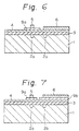
- Figure 7 shows a structure of a first modification, which is an improvement of the example of Fig. 6.
- a semiconductive layer 9b comprised of silicon (Si) is added to the structure shown in Fig. 6.
- the semiconductive layer 9b is formed between the semiconductive layer 4 and the electrode 6.
- the semiconductive layer 9b has a specific resistance different from that of the semiconductive layers 4, 9a and has a broader width than that of the corresponding electrode 6. Since the present device has a number of design parameters, it is possible to design and optimize the device more effectively and thus gain a better effect.
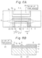
- Figures 8A and 8B show a structure of a second modification.
- the structure of Figs. 8A and 8B has a semiconductive layer 9c, comprising silicon (Si), on which a third electrode 10 is formed, the layer 9c being separated from the layer 9a in a region between the electrodes 5 and 10.
- the semiconductive layer 9c has a specific resistance different from that of the semiconductive layer 4 and has a broader width than that of the electrode 10. According to this structure, it is possible to suppress a DC drift of the device and thus effectively compensate for a fluctuation in operational characteristics due to the DC drift, stress, or the like.
- the present invention is applicable to other optical waveguide devices such as optical switches, or the like. Also, the present invention can be applied to an optical waveguide device to which a low frequency signal and a high frequency signal are fed independently.
Landscapes
- Physics & Mathematics (AREA)
- Nonlinear Science (AREA)
- General Physics & Mathematics (AREA)
- Optics & Photonics (AREA)
- Chemical & Material Sciences (AREA)
- Engineering & Computer Science (AREA)
- Ceramic Engineering (AREA)
- Crystallography & Structural Chemistry (AREA)
- Optical Modulation, Optical Deflection, Nonlinear Optics, Optical Demodulation, Optical Logic Elements (AREA)
- Optical Integrated Circuits (AREA)
Claims (10)
- Dispositif de guide d'onde optique comprenant :un guide d'onde optique (2, 2a, 2b) formé sur une surface d'un substrat (1) ayant un effet électro-optique ;une paire d'électrodes (5, 6) connectées de façon fonctionnelle et agencées pour recevoir entre elles un signal électrique d'attaque ;une couche tampon (3) formée sur toute ladite surface dudit substrat (1) y compris le guide d'onde optique (2, 2a, 2b) ; etune couche semi-conductrice (4) formée entre la couche tampon (3) et la paire d'électrodes (5, 6), une partie (P ; Q) de ladite couche semi-conductrice (4a, 4b ; 4c) qui correspond à l'espace entre la paire d'électrodes (5, 6) étant d'une épaisseur réduite ou nulle ;dans lequel une variation de fréquence du signal électrique d'attaque appliqué entre la paire d'électrodes (5, 6), lorsque le dispositif est en utilisation, provoque une variation correspondante de la répartition d'un champ électrique qui apparaít au voisinage du guide d'onde optique (2, 2a, 2b), et dans lequel, lorsque l'on applique un signal électrique à basse fréquence à la paire d'électrodes (5, 6), le champ électrique est concentré sur ladite partie (P ; Q) de ladite couche semi-conductrice (4a, 4b ; 4c).
- Dispositif de guide d'onde optique selon la revendication 1, dans lequel la couche semi-conductrice (4c) comporte une partie (Q) formée finement et est formée seulement au voisinage de la paire d'électrodes (5, 6).
- Dispositif de guide d'onde optique selon la revendication 1, dans lequel, lorsque l'épaisseur de ladite couche semi-conductrice (4a, 4b) au niveau de ladite partie (P) est nulle, la couche semi-conductrice (4a, 4b) comprend deux régions séparées l'une de l'autre au niveau d'une partie de ladite couche correspondant à l'espace entre ladite paire d'électrodes (5, 6), chaque région séparée de la couche semi-conductrice (4a, 4b) ayant une largeur plus grande que celle de ladite paire d'électrodes (5, 6) sous laquelle elle se trouve.
- Dispositif de guide d'onde optique selon la revendication 3, dans lequel celle (4a) des régions séparées (4a, 4b) de la couche semi-conductrice qui se trouve sous une électrode (5) de ligne de signal de la paire d'électrodes (5, 6) est formée seulement au voisinage de l'électrode (5) de ligne de signal.
- Dispositif de guide d'onde optique comprenant :un guide d'onde optique (2, 2a, 2b) formé sur une surface d'un substrat (1) ayant un effet électro-optique ;une paire d'électrodes (5, 6) connectées de façon fonctionnelle et agencées pour recevoir entre elles un signal électrique d'attaque ;une couche tampon (3) formée sur toute ladite surface dudit substrat (1) y compris le guide d'onde optique (2, 2a, 2b) ; etune première couche semi-conductrice (4) formée entre la couche tampon (3) et la paire d'électrodes (5, 6), et une seconde couche semi-conductrice (9a), formée entre la première couche semi-conductrice (4) et une électrode (5) de ligne de signal de la paire d'électrodes (5, 6), la seconde couche semi-conductrice (9a) ayant une résistance spécifique différente de celle de la première couche semi-conductrice (4) et ayant une largeur plus grande que celle de l'électrode (5) de ligne de signal ;dans lequel une variation de fréquence d'un signal électrique d'attaque appliqué entre les deux, lorsque le dispositif est en utilisation, provoque une variation correspondante de la répartition d'un champ électrique qui apparaít au voisinage du guide d'onde optique (2, 2a, 2b).
- Dispositif de guide d'onde optique selon la revendication 5, dans lequel une deuxième couche semi-conductrice (9b) est aussi formée entre la première couche semi-conductrice (4) et l'électrode (6) de mise à la masse de la paire d'électrodes (5, 6), de façon qu'il y ait deux régions (9a, 9b) de couche semi-conductrice séparées l'une de l'autre au niveau d'un emplacement correspondant à l'espace entre la paire d'électrodes (5, 6), chaque région séparée (9a, 9b) ayant une largeur plus grande que celle de l'électrode, de ladite paire d'électrodes (5, 6), sous laquelle elle se trouve.
- Dispositif de guide d'onde optique selon la revendication 6, comprenant en outre une troisième électrode (10), dans lequel une seconde couche semi-conductrice (9c) est aussi formée entre la première couche semi-conductrice (4) et ladite troisième électrode (10), de façon qu'il y ait trois régions (9a, 9b, 9c) de couche semi-conductrice séparées les unes des autres au niveau d'emplacements respectifs correspondant aux espaces entre les trois électrodes (5, 6, 10), chaque région séparée (9a, 9b, 9c) ayant une largeur plus grande que celle de l'électrode, desdites électrodes (5, 6, 10), sous laquelle elle se trouve.
- Dispositif de guide d'onde optique selon l'une quelconque des revendications précédentes, dans lequel la couche tampon (3) est composée d'une matière diélectrique et a un indice de réfraction plus petit que celui du guide d'onde optique (2, 2a, 2b).
- Dispositif de guide d'onde optique selon la revendication 8, dans lequel la matière diélectrique comprend du dioxyde de silicium.
- Dispositif de guide d'onde optique selon l'une quelconque des revendications précédentes, dans lequel la, ou chaque, couche semi-conductrice (4 ; 9a, 9b) comprend du silicium.
Priority Applications (1)
| Application Number | Priority Date | Filing Date | Title |
|---|---|---|---|
| EP00108030A EP1022605B1 (fr) | 1990-03-02 | 1991-03-01 | Dispositif optique à guide d'onde |
Applications Claiming Priority (4)
| Application Number | Priority Date | Filing Date | Title |
|---|---|---|---|
| JP5202290 | 1990-03-02 | ||
| JP52022/90 | 1990-03-02 | ||
| JP2052022A JP2867560B2 (ja) | 1990-03-02 | 1990-03-02 | 光導波路デバイス |
| EP91301729A EP0444959B1 (fr) | 1990-03-02 | 1991-03-01 | Dispositif optique à guide d'onde |
Related Parent Applications (2)
| Application Number | Title | Priority Date | Filing Date |
|---|---|---|---|
| EP91301729A Division EP0444959B1 (fr) | 1990-03-02 | 1991-03-01 | Dispositif optique à guide d'onde |
| EP91301729.9 Division | 1991-03-01 |
Related Child Applications (1)
| Application Number | Title | Priority Date | Filing Date |
|---|---|---|---|
| EP00108030A Division EP1022605B1 (fr) | 1990-03-02 | 1991-03-01 | Dispositif optique à guide d'onde |
Publications (3)
| Publication Number | Publication Date |
|---|---|
| EP0677765A2 EP0677765A2 (fr) | 1995-10-18 |
| EP0677765A3 EP0677765A3 (fr) | 1996-01-31 |
| EP0677765B1 true EP0677765B1 (fr) | 2001-07-25 |
Family
ID=12903190
Family Applications (3)
| Application Number | Title | Priority Date | Filing Date |
|---|---|---|---|
| EP00108030A Expired - Lifetime EP1022605B1 (fr) | 1990-03-02 | 1991-03-01 | Dispositif optique à guide d'onde |
| EP91301729A Expired - Lifetime EP0444959B1 (fr) | 1990-03-02 | 1991-03-01 | Dispositif optique à guide d'onde |
| EP95108382A Expired - Lifetime EP0677765B1 (fr) | 1990-03-02 | 1991-03-01 | Dispositif optique à guide d'onde |
Family Applications Before (2)
| Application Number | Title | Priority Date | Filing Date |
|---|---|---|---|
| EP00108030A Expired - Lifetime EP1022605B1 (fr) | 1990-03-02 | 1991-03-01 | Dispositif optique à guide d'onde |
| EP91301729A Expired - Lifetime EP0444959B1 (fr) | 1990-03-02 | 1991-03-01 | Dispositif optique à guide d'onde |
Country Status (4)
| Country | Link |
|---|---|
| US (1) | US5214724A (fr) |
| EP (3) | EP1022605B1 (fr) |
| JP (1) | JP2867560B2 (fr) |
| DE (3) | DE69133344T2 (fr) |
Cited By (1)
| Publication number | Priority date | Publication date | Assignee | Title |
|---|---|---|---|---|
| US7082237B2 (en) | 2002-01-19 | 2006-07-25 | Bookham Technology, Plc | Optical modulators operated in parallel push-pull mode |
Families Citing this family (43)
| Publication number | Priority date | Publication date | Assignee | Title |
|---|---|---|---|---|
| JPH04179931A (ja) * | 1990-11-14 | 1992-06-26 | Oki Electric Ind Co Ltd | 導波型光デバイス |
| US5404412A (en) * | 1991-12-27 | 1995-04-04 | Fujitsu Limited | Optical waveguide device |
| US5339369A (en) * | 1992-10-23 | 1994-08-16 | General Microwave Israel Corporation | High-speed external modulator |
| US5455876A (en) * | 1992-10-23 | 1995-10-03 | General Microwave Israel Corporation | High-speed external integrated optical modulator |
| JP2713087B2 (ja) * | 1993-04-13 | 1998-02-16 | 日本電気株式会社 | 導波形光デバイス |
| JP2555942B2 (ja) * | 1993-08-27 | 1996-11-20 | 日本電気株式会社 | 光制御デバイス |
| JP3628342B2 (ja) * | 1993-09-17 | 2005-03-09 | 富士通株式会社 | 誘電体光導波路デバイス |
| CA2133300C (fr) * | 1993-11-01 | 1999-04-27 | Hirotoshi Nagata | Dispositif a guide de lumiere |
| JP3771287B2 (ja) * | 1994-04-15 | 2006-04-26 | 富士写真フイルム株式会社 | 導波路型電気光学素子 |
| US5617500A (en) * | 1994-05-20 | 1997-04-01 | Nikon Corporation | System for detecting an optical information and scanning microscope system |
| JPH0815657A (ja) * | 1994-07-01 | 1996-01-19 | Fuji Photo Film Co Ltd | 導波路型電気光学素子 |
| JP2606674B2 (ja) * | 1994-10-27 | 1997-05-07 | 日本電気株式会社 | 導波形光デバイス |
| JP2894961B2 (ja) * | 1994-11-18 | 1999-05-24 | 日本電気株式会社 | 光制御デバイス |
| JP3043614B2 (ja) * | 1996-05-10 | 2000-05-22 | 日本電気株式会社 | 導波路型光デバイス |
| JP2873203B2 (ja) * | 1996-06-14 | 1999-03-24 | 住友大阪セメント株式会社 | 導波路型光デバイス |
| US5991491A (en) * | 1996-11-08 | 1999-11-23 | Nec Corporation | Optical waveguide type device for reducing microwave attenuation |
| JP2850899B2 (ja) * | 1997-04-21 | 1999-01-27 | 日本電気株式会社 | 光制御デバイス |
| JP3237620B2 (ja) * | 1998-08-25 | 2001-12-10 | 日本電気株式会社 | 光制御デバイスおよびその製造方法 |
| EP1197784A4 (fr) * | 1999-06-28 | 2004-03-24 | Sumitomo Osaka Cement Co Ltd | Composant optoelectronique et son procede de fabrication |
| JP4309571B2 (ja) * | 2000-12-27 | 2009-08-05 | 住友大阪セメント株式会社 | 光導波路素子 |
| GB2374945A (en) * | 2001-04-26 | 2002-10-30 | Jds Uniphase Corp | Mach-Zehnder Optical Modulator |
| JPWO2002097521A1 (ja) | 2001-05-25 | 2004-09-16 | アンリツ株式会社 | 熱ドリフトを効果的に抑圧して優れた電気的特性を有する光変調デバイス及びその製造方法 |
| JP2004046283A (ja) * | 2001-05-25 | 2004-02-12 | Anritsu Corp | 熱ドリフトを効果的に抑圧して優れた電気的特性を有する光変調デバイス及びその製造方法 |
| EP1271221A1 (fr) * | 2001-06-28 | 2003-01-02 | Corning O.T.I. S.p.A. | Dispositif de guide d'onde optique intégré |
| US20030031400A1 (en) * | 2001-06-28 | 2003-02-13 | Valerio Pruneri | Integrated optical waveguide device |
| JP2003057616A (ja) * | 2001-07-25 | 2003-02-26 | Corlux Corp | 光導波路素子、光変調器及び光通信システム |
| JP3640390B2 (ja) * | 2002-09-12 | 2005-04-20 | 住友大阪セメント株式会社 | 光変調器 |
| US6845183B2 (en) * | 2003-02-05 | 2005-01-18 | Jds Uniphase Corporation | Slotted electrode electro-optic modulator |
| JP2005070460A (ja) * | 2003-08-25 | 2005-03-17 | Eudyna Devices Inc | 光半導体装置、光位相制御装置、光強度制御装置及び光半導体装置の製造方法 |
| JP4927358B2 (ja) * | 2004-07-27 | 2012-05-09 | ジェイディーエス ユニフェイズ コーポレーション | バッファ層を有する低バイアス・ドリフト変調器 |
| US7405861B2 (en) | 2004-09-27 | 2008-07-29 | Idc, Llc | Method and device for protecting interferometric modulators from electrostatic discharge |
| US7844149B2 (en) * | 2007-01-12 | 2010-11-30 | Jds Uniphase Corporation | Humidity tolerant electro-optic device |
| US7719752B2 (en) | 2007-05-11 | 2010-05-18 | Qualcomm Mems Technologies, Inc. | MEMS structures, methods of fabricating MEMS components on separate substrates and assembly of same |
| US7856156B2 (en) * | 2008-08-22 | 2010-12-21 | The Boeing Company | Lithium niobate modulator having a doped semiconductor structure for the mitigation of DC bias drift |
| US9020306B2 (en) | 2013-03-14 | 2015-04-28 | The Aerospace Corporation | Stable lithium niobate waveguide devices, and methods of making and using same |
| CN104076973A (zh) * | 2013-03-26 | 2014-10-01 | Lg伊诺特有限公司 | 触控面板和具有该触控面板的触控设备 |
| US9575340B2 (en) | 2015-02-24 | 2017-02-21 | Ii-Vi Incorporated | Electrode configuration for electro-optic modulators |
| JP6561383B2 (ja) * | 2017-03-31 | 2019-08-21 | 住友大阪セメント株式会社 | 光変調素子 |
| CN108303377B (zh) * | 2018-02-02 | 2023-05-09 | 成都信息工程大学 | 一种热光效应光波导检测装置 |
| CN108051406B (zh) * | 2018-02-02 | 2023-05-09 | 成都信息工程大学 | 一种电光效应光波导检测装置 |
| JP2020134875A (ja) * | 2019-02-25 | 2020-08-31 | 富士通オプティカルコンポーネンツ株式会社 | 光変調器 |
| CN109975618B (zh) * | 2019-03-01 | 2021-11-19 | 昆明理工大学 | 抑制直流漂移的集成光波导电场传感芯片、系统及方法 |
| CN109920694B (zh) * | 2019-03-14 | 2021-04-20 | 北海银河开关设备有限公司 | 一种铁路高压接地开关极柱 |
Family Cites Families (11)
| Publication number | Priority date | Publication date | Assignee | Title |
|---|---|---|---|---|
| US4679893A (en) * | 1983-08-26 | 1987-07-14 | Hughes Aircraft Company | High switching frequency optical waveguide switch, modulator, and filter devices |
| FR2558270B1 (fr) * | 1984-01-18 | 1986-04-25 | Comp Generale Electricite | Modulateur electro-optique interferentiel a haute sensibilite |
| US4684207A (en) * | 1985-04-30 | 1987-08-04 | Lawless William N | Field dependent electrooptic device and method |
| JPS6273207A (ja) * | 1985-09-27 | 1987-04-03 | Fujitsu Ltd | 導波路光デイバイス |
| JPS62173428A (ja) * | 1986-01-28 | 1987-07-30 | Fujitsu Ltd | 導波路光デバイス |
| GB2193337B (en) * | 1986-07-30 | 1990-03-07 | Gen Electric Plc | Optical switch apparatus |
| JP2581731B2 (ja) * | 1988-02-18 | 1997-02-12 | 富士通株式会社 | 導波路形光デバイス及びその製造方法 |
| JPH01302325A (ja) * | 1988-05-31 | 1989-12-06 | Fujitsu Ltd | 光導波路デバイスおよびその形成方法 |
| US5002353A (en) * | 1989-04-25 | 1991-03-26 | Massachusetts Institute Of Technology | Apparatus and method for reducing modulator nonlinearities |
| US4936644A (en) * | 1989-06-13 | 1990-06-26 | Hoechst Celanese Corp. | Polarization-insensitive interferometric waveguide electrooptic modulator |
| US4932738A (en) * | 1989-06-13 | 1990-06-12 | Hoechst Celanese Corp. | Polarization-insensitive interferometric waveguide electrooptic modulator |
-
1990
- 1990-03-02 JP JP2052022A patent/JP2867560B2/ja not_active Expired - Lifetime
-
1991
- 1991-02-28 US US07/661,602 patent/US5214724A/en not_active Expired - Lifetime
- 1991-03-01 DE DE69133344T patent/DE69133344T2/de not_active Expired - Lifetime
- 1991-03-01 EP EP00108030A patent/EP1022605B1/fr not_active Expired - Lifetime
- 1991-03-01 EP EP91301729A patent/EP0444959B1/fr not_active Expired - Lifetime
- 1991-03-01 EP EP95108382A patent/EP0677765B1/fr not_active Expired - Lifetime
- 1991-03-01 DE DE69132673T patent/DE69132673T2/de not_active Expired - Fee Related
- 1991-03-01 DE DE69123066T patent/DE69123066D1/de not_active Expired - Lifetime
Cited By (1)
| Publication number | Priority date | Publication date | Assignee | Title |
|---|---|---|---|---|
| US7082237B2 (en) | 2002-01-19 | 2006-07-25 | Bookham Technology, Plc | Optical modulators operated in parallel push-pull mode |
Also Published As
| Publication number | Publication date |
|---|---|
| EP1022605B1 (fr) | 2003-12-03 |
| EP1022605A3 (fr) | 2000-08-16 |
| EP0444959B1 (fr) | 1996-11-13 |
| US5214724A (en) | 1993-05-25 |
| EP0677765A2 (fr) | 1995-10-18 |
| EP0444959A3 (en) | 1992-05-27 |
| JP2867560B2 (ja) | 1999-03-08 |
| DE69132673T2 (de) | 2002-04-18 |
| JPH03253815A (ja) | 1991-11-12 |
| DE69132673D1 (de) | 2001-08-30 |
| DE69123066D1 (de) | 1996-12-19 |
| DE69133344D1 (de) | 2004-01-15 |
| EP0677765A3 (fr) | 1996-01-31 |
| EP1022605A2 (fr) | 2000-07-26 |
| DE69133344T2 (de) | 2004-05-27 |
| EP0444959A2 (fr) | 1991-09-04 |
Similar Documents
| Publication | Publication Date | Title |
|---|---|---|
| EP0677765B1 (fr) | Dispositif optique à guide d'onde | |
| US7408693B2 (en) | Electro-optic device | |
| US5138480A (en) | Traveling wave optical modulator | |
| US7324257B2 (en) | Low bias drift modulator with buffer layer | |
| US7912326B2 (en) | Optical control device | |
| EP2133733B1 (fr) | Modulateur optique à base de l'effet électro-optique | |
| US20080170818A1 (en) | Humidity Tolerant Electro-Optic Device | |
| US5748358A (en) | Optical modulator with optical waveguide and traveling-wave type electrodes | |
| CN113646690B (zh) | 光调制器 | |
| WO2001086824A3 (fr) | Modulateur d'intensite linbo3 a faible tension de commande avec pertes reduites dans les electrodes | |
| EP0153312A1 (fr) | Dispositif de filtre électro-optique. | |
| US20030016896A1 (en) | Electro-optic waveguide devices | |
| US6891982B2 (en) | Optical modulation device having excellent electric characteristics by effectively restricting heat drift | |
| JPH08166566A (ja) | 光制御デバイス | |
| JP2006317550A (ja) | 光変調器 | |
| JPH0829745A (ja) | 光導波路デバイス | |
| JP4227595B2 (ja) | 光変調器 | |
| JPH1054961A (ja) | 光制御デバイスおよび光制御装置 | |
| JPH09281454A (ja) | 導波路型光変調器 | |
| JPH1054962A (ja) | 光制御装置および光制御デバイス | |
| JP2004046283A (ja) | 熱ドリフトを効果的に抑圧して優れた電気的特性を有する光変調デバイス及びその製造方法 | |
| HK1004959A (en) | Optical waveguide modulator with traveling-wave type electrodes | |
| JPH1048584A (ja) | 光制御デバイスの製作方法 | |
| JPH0731333B2 (ja) | 光導波路型デバイス | |
| JP2006317551A (ja) | 光変調器 |
Legal Events
| Date | Code | Title | Description |
|---|---|---|---|
| PUAI | Public reference made under article 153(3) epc to a published international application that has entered the european phase |
Free format text: ORIGINAL CODE: 0009012 |
|
| AC | Divisional application: reference to earlier application |
Ref document number: 444959 Country of ref document: EP |
|
| AK | Designated contracting states |
Kind code of ref document: A2 Designated state(s): DE FR GB SE |
|
| RIN1 | Information on inventor provided before grant (corrected) |
Inventor name: DOI,MASAHARU, C/O FUJITSU LIMITED Inventor name: KUBOTA, YOSHINOBU Inventor name: NAKAZAWA, TADAO Inventor name: MEKADA,NAOYUKI, C/O FUJITSU LIMITED Inventor name: SEINO,MINORU, C/O FUJITSU LIMITED |
|
| PUAL | Search report despatched |
Free format text: ORIGINAL CODE: 0009013 |
|
| AK | Designated contracting states |
Kind code of ref document: A3 Designated state(s): DE FR GB SE |
|
| 17P | Request for examination filed |
Effective date: 19960625 |
|
| GRAG | Despatch of communication of intention to grant |
Free format text: ORIGINAL CODE: EPIDOS AGRA |
|
| 17Q | First examination report despatched |
Effective date: 19991011 |
|
| GRAG | Despatch of communication of intention to grant |
Free format text: ORIGINAL CODE: EPIDOS AGRA |
|
| GRAG | Despatch of communication of intention to grant |
Free format text: ORIGINAL CODE: EPIDOS AGRA |
|
| GRAH | Despatch of communication of intention to grant a patent |
Free format text: ORIGINAL CODE: EPIDOS IGRA |
|
| GRAH | Despatch of communication of intention to grant a patent |
Free format text: ORIGINAL CODE: EPIDOS IGRA |
|
| GRAA | (expected) grant |
Free format text: ORIGINAL CODE: 0009210 |
|
| AC | Divisional application: reference to earlier application |
Ref document number: 444959 Country of ref document: EP |
|
| AK | Designated contracting states |
Kind code of ref document: B1 Designated state(s): DE FR GB SE |
|
| REF | Corresponds to: |
Ref document number: 69132673 Country of ref document: DE Date of ref document: 20010830 |
|
| EN | Fr: translation not filed | ||
| REG | Reference to a national code |
Ref country code: GB Ref legal event code: IF02 |
|
| PG25 | Lapsed in a contracting state [announced via postgrant information from national office to epo] |
Ref country code: SE Free format text: LAPSE BECAUSE OF NON-PAYMENT OF DUE FEES Effective date: 20020302 |
|
| EN | Fr: translation not filed |
Free format text: BO 01/51 PAGES: 265, IL Y A LIEU DE SUPPRIMER: LA MENTION DE LA NON REMISE. LA REMISE EST PUBLIEE DANS LE PRESENT BOPI. |
|
| ET | Fr: translation filed | ||
| PLBE | No opposition filed within time limit |
Free format text: ORIGINAL CODE: 0009261 |
|
| STAA | Information on the status of an ep patent application or granted ep patent |
Free format text: STATUS: NO OPPOSITION FILED WITHIN TIME LIMIT |
|
| 26N | No opposition filed | ||
| PG25 | Lapsed in a contracting state [announced via postgrant information from national office to epo] |
Ref country code: DE Free format text: LAPSE BECAUSE OF NON-PAYMENT OF DUE FEES Effective date: 20021001 |
|
| EUG | Se: european patent has lapsed |
Ref document number: 95108382.3 |
|
| PGFP | Annual fee paid to national office [announced via postgrant information from national office to epo] |
Ref country code: FR Payment date: 20100324 Year of fee payment: 20 |
|
| PGFP | Annual fee paid to national office [announced via postgrant information from national office to epo] |
Ref country code: GB Payment date: 20100224 Year of fee payment: 20 |
|
| REG | Reference to a national code |
Ref country code: GB Ref legal event code: PE20 Expiry date: 20110228 |
|
| PG25 | Lapsed in a contracting state [announced via postgrant information from national office to epo] |
Ref country code: GB Free format text: LAPSE BECAUSE OF EXPIRATION OF PROTECTION Effective date: 20110228 |