EP0678904A1 - Wafer-Schneidverfahren durch Mehrfachschnitte - Google Patents
Wafer-Schneidverfahren durch Mehrfachschnitte Download PDFInfo
- Publication number
- EP0678904A1 EP0678904A1 EP19950302264 EP95302264A EP0678904A1 EP 0678904 A1 EP0678904 A1 EP 0678904A1 EP 19950302264 EP19950302264 EP 19950302264 EP 95302264 A EP95302264 A EP 95302264A EP 0678904 A1 EP0678904 A1 EP 0678904A1
- Authority
- EP
- European Patent Office
- Prior art keywords
- cut
- wafer
- scribing
- semiconductor wafer
- scribe line
- Prior art date
- Legal status (The legal status is an assumption and is not a legal conclusion. Google has not performed a legal analysis and makes no representation as to the accuracy of the status listed.)
- Ceased
Links
Images



Classifications
-
- H—ELECTRICITY
- H10—SEMICONDUCTOR DEVICES; ELECTRIC SOLID-STATE DEVICES NOT OTHERWISE PROVIDED FOR
- H10P—GENERIC PROCESSES OR APPARATUS FOR THE MANUFACTURE OR TREATMENT OF DEVICES COVERED BY CLASS H10
- H10P52/00—Grinding, lapping or polishing of wafers, substrates or parts of devices
-
- H—ELECTRICITY
- H10—SEMICONDUCTOR DEVICES; ELECTRIC SOLID-STATE DEVICES NOT OTHERWISE PROVIDED FOR
- H10D—INORGANIC ELECTRIC SEMICONDUCTOR DEVICES
- H10D62/00—Semiconductor bodies, or regions thereof, of devices having potential barriers
- H10D62/10—Shapes, relative sizes or dispositions of the regions of the semiconductor bodies; Shapes of the semiconductor bodies
- H10D62/117—Shapes of semiconductor bodies
-
- Y—GENERAL TAGGING OF NEW TECHNOLOGICAL DEVELOPMENTS; GENERAL TAGGING OF CROSS-SECTIONAL TECHNOLOGIES SPANNING OVER SEVERAL SECTIONS OF THE IPC; TECHNICAL SUBJECTS COVERED BY FORMER USPC CROSS-REFERENCE ART COLLECTIONS [XRACs] AND DIGESTS
- Y10—TECHNICAL SUBJECTS COVERED BY FORMER USPC
- Y10T—TECHNICAL SUBJECTS COVERED BY FORMER US CLASSIFICATION
- Y10T225/00—Severing by tearing or breaking
- Y10T225/10—Methods
- Y10T225/12—With preliminary weakening
-
- Y—GENERAL TAGGING OF NEW TECHNOLOGICAL DEVELOPMENTS; GENERAL TAGGING OF CROSS-SECTIONAL TECHNOLOGIES SPANNING OVER SEVERAL SECTIONS OF THE IPC; TECHNICAL SUBJECTS COVERED BY FORMER USPC CROSS-REFERENCE ART COLLECTIONS [XRACs] AND DIGESTS
- Y10—TECHNICAL SUBJECTS COVERED BY FORMER USPC
- Y10T—TECHNICAL SUBJECTS COVERED BY FORMER US CLASSIFICATION
- Y10T83/00—Cutting
- Y10T83/02—Other than completely through work thickness
-
- Y—GENERAL TAGGING OF NEW TECHNOLOGICAL DEVELOPMENTS; GENERAL TAGGING OF CROSS-SECTIONAL TECHNOLOGIES SPANNING OVER SEVERAL SECTIONS OF THE IPC; TECHNICAL SUBJECTS COVERED BY FORMER USPC CROSS-REFERENCE ART COLLECTIONS [XRACs] AND DIGESTS
- Y10—TECHNICAL SUBJECTS COVERED BY FORMER USPC
- Y10T—TECHNICAL SUBJECTS COVERED BY FORMER US CLASSIFICATION
- Y10T83/00—Cutting
- Y10T83/02—Other than completely through work thickness
- Y10T83/0304—Grooving
Definitions
- the present invention relates generally to a method for cutting a plate-like material and, more specifically, to a method of cutting a semiconductor wafer that contains metal deposits along a scribe line.
- multiple semiconductor devices are typically arranged on one surface of a round silicon wafer. It is known to separate or dice the multiple semiconductor devices with a diamond coated saw blade along the scribe line.
- semiconductor wafers may have test patterns deposited along the scribe line on the surface of the wafer. These test patterns may be composed of metal and have a width wider than the width of the standard diamond saw blade. After the wafer is cut, metal may remain on the edge of the cut and metal slivers may subsequently become dislodged. The slivers can interfere with the operation of the semiconductor device and thus affect the reliability of the device.
- the present invention provides a method for cutting semiconductor wafers that contain test patterns on the scribe lines without producing slivers.
- the present invention uses multiple scribing cuts to remove the excess test pattern material, followed by a severing cut to dice the semiconductor wafer along the scribe line and remove any test pattern material that may remain.
- test patterns are removed by scribing cuts made with a beveled or V-shaped blade.
- the semiconductor wafer is then severed along the scribe line with a standard flat surface saw blade.
- Figs. 1A and 1B show a prior art method of cutting a semiconductor wafer.
- a semiconductor wafer 10 has a metal test pattern 12 deposited on the surface of the wafer.
- the test pattern may be deposited along an area known as a scribe line.
- a scribe line or street is the area between semiconductor devices where a diamond saw blade 13 will sever or dice the semiconductor wafer.
- the saw blade will generally have a width less than the width of the scribe line.
- the saw blade has a blade thickness of 1.2 to 1.6 mil.
- the semiconductor wafer is shown having a layer of mounting tape 14 taped to the underside of the wafer.
- the mounting tape is attached to a frame (not shown) and secures the wafer die both during and after the cutting process.
- the saw blade does not sever the mounting tape.
- Fig. 1B shows the semiconductor wafer after it has been cut according to the prior art.
- the cut severs the semiconductor wafer in the middle of the scribe line creating a groove 16.
- the width of the test patterns may be wider than the saw blade, two portions of test pattern 12 remain on the top surface of the wafer near groove 16. These portions of the test pattern may become dislodged as slivers and affect the reliability of the packaged semiconductor device. This is especially true when the test pattern is composed of a conducting material because the slivers may short out the semiconductor device.
- two scribing cuts are used to eliminate portions of the test pattern and a third severing cut dices the wafer, removing whatever portion, if any, of the test pattern that remains.
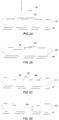
- a semiconductor wafer 30 has a metal test pattern 32 deposited along the scribe line on the surface of the wafer.
- a standard flat surface saw blade 33 is used to cut the wafer.
- a mounting tape 34 is taped to the underside of the semiconductor wafer and attached to a frame (not shown).
- a first scribing cut is made in the semiconductor wafer on one side of the scribe line to remove a first portion of test pattern 32.
- Fig. 2B shows the wafer after the first scribing cut which leaves a groove 36.
- a second scribing cut is made in the semiconductor wafer on the other side of the scribe line to remove a second portion of test pattern 32.
- the second cut leaves a groove 38 and is shown in Fig. 2C.
- Neither the first or second scribing cuts sever the wafer and are only intended to remove portions of the test pattern outside the width of the saw blade.
- the first and second cuts may be superficial.
- a third severing cut is then made along the center of the scribe line to sever the wafer.
- Fig. 2D shows the wafer after the third cut which leaves a groove 39. The cut severs the wafer but does not sever mounting tape 34.
- the description and figures show the third severing cut passing through the wafer, the present invention may also be practiced where the third cut does not sever the wafer.
- the wafer may then be broken along the scribe line in any number of ways known to those skilled in the art.
- cut depth max. feed speed first cut 3 mils 0.5 in./second second cut 3 mils 0.5 in./second third cut 18.5 mils 2.5 in./second These settings are for a standard semiconductor wafer and may be modified for other uses.
- two scribing cuts are made with a beveled or V-shaped saw blade to remove the test pattern.
- a third severing cut is made with a standard flat surface blade to sever the wafer.
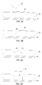
- a semiconductor wafer 60 has a metal test pattern 62 deposited along the scribe line on the surface of the wafer.
- a V-shaped saw blade 63 is used to scribe the wafer along the scribe line.
- a mounting tape 64 is taped to the underside of the semiconductor wafer.
- a first scribing cut is made in the semiconductor wafer along one half of the scribe line to remove a first portion of test pattern 62.
- Fig. 3B shows the wafer after the first scribing cut which leaves a groove 68.
- a second scribing cut is made in the semiconductor wafer along the other half of the scribe line to remove a second portion of test pattern 62.
- the second scribing cut leaves a groove 70 and is shown in Fig. 3C. Neither the first or second scribing cuts sever the wafer and are only intended to remove the test pattern.
- a third severing cut is then made along the scribe line to sever the wafer.
- Fig. 3D shows the wafer after the third severing cut.
- the third cut may be made with a standard flat surface saw blade 72 leaving a groove 74.
- the third cut severs the wafer but does not sever mounting tape 64.
- This embodiment has the advantage of producing beveled top edges along the scribe line. Beveled edges help reduce semiconductor wafer chipping.
- one scribing cut is made with a V-shaped saw blade to remove the test pattern.
- the saw blade has a thickness greater than the width of the test pattern.
- a second severing cut is made with a flat surface saw blade to sever the wafer.
- a semiconductor wafer 80 has a metal test pattern 82 deposited along the scribe line on the surface of the wafer.
- a V-shaped saw blade 83 is used to scribe the wafer along the scribe line.
- the saw blade has a thickness greater than the width of the test pattern so only one cut is needed to scribe the test pattern.
- a mounting tape 84 is taped to the underside of the semiconductor wafer.
- a first scribing cut is made in the semiconductor wafer to remove test pattern 82.
- Fig. 4B shows the wafer after the first scribing cut which leaves a groove 86. Then a second severing cut is made along the scribe line to dice the wafer.
- Fig. 4C shows a flat surface saw blade 88 may be used to make the second severing cut.
- Fig. 4D shows the wafer after the second severing cut which leaves a groove 90.
- the second severing cut severs the wafer but does not sever mounting tape 84.
- This embodiment also has the advantage of producing beveled top edges along the scribe line which may help reduce semiconductor wafer chipping.
- the present invention may also be practiced where a single scribing/severing cut is made with a V-shaped saw blade which has a thickness greater than the width of the test pattern. This method is shown in Figs. 5A and 5B.
- a semiconductor wafer 100 has a metal test pattern 102 deposited along the scribe line on the surface of the wafer.
- a V-shaped saw blade 103 is used to scribe and sever the wafer along the scribe line. As the saw blade has a thickness greater than the width of the test pattern, the severing cut can also scribe the test pattern.
- a mounting tape 104 is taped to the underside of the semiconductor wafer.
- a first scribing/severing cut is made in the semiconductor wafer to remove test pattern 102 and sever the wafer.
- Fig. 4B shows the wafer after the first scribing/severing cut which leaves a groove 106.
- the scribing/severing cut severs the wafer but does not sever mounting tape 104.
- This embodiment also has the advantage of producing beveled top edges along the scribe line which may help reduce semiconductor wafer chipping.
Landscapes
- Dicing (AREA)
- Processing Of Stones Or Stones Resemblance Materials (AREA)
Applications Claiming Priority (4)
| Application Number | Priority Date | Filing Date | Title |
|---|---|---|---|
| US22590494A | 1994-04-12 | 1994-04-12 | |
| US225904 | 1994-04-12 | ||
| US23363094A | 1994-04-26 | 1994-04-26 | |
| US233630 | 1994-04-26 |
Publications (1)
| Publication Number | Publication Date |
|---|---|
| EP0678904A1 true EP0678904A1 (de) | 1995-10-25 |
Family
ID=26920026
Family Applications (1)
| Application Number | Title | Priority Date | Filing Date |
|---|---|---|---|
| EP19950302264 Ceased EP0678904A1 (de) | 1994-04-12 | 1995-04-05 | Wafer-Schneidverfahren durch Mehrfachschnitte |
Country Status (3)
| Country | Link |
|---|---|
| US (1) | US5786266A (de) |
| EP (1) | EP0678904A1 (de) |
| JP (1) | JPH0845879A (de) |
Cited By (2)
| Publication number | Priority date | Publication date | Assignee | Title |
|---|---|---|---|---|
| EP0844648A4 (de) * | 1996-06-07 | 1998-06-17 | ||
| EP0822430A3 (de) * | 1996-07-31 | 1999-04-28 | Nippon Telegraph And Telephone Corporation | Optischer Ablenker in einem Lichtwellenleiter, Verfahren zur dessen Herstellung, und Sägeblatt zur Verwendung bei diesem Verfahren |
Families Citing this family (42)
| Publication number | Priority date | Publication date | Assignee | Title |
|---|---|---|---|---|
| JPH09172223A (ja) * | 1995-12-19 | 1997-06-30 | Sony Corp | 半導体装置と半導体装置の製造方法 |
| JPH1027971A (ja) * | 1996-07-10 | 1998-01-27 | Nec Corp | 有機薄膜多層配線基板の切断方法 |
| NL1004016C2 (nl) * | 1996-09-12 | 1998-03-13 | Oce Tech Bv | Inktstraal-drukkop. |
| US6127245A (en) * | 1997-02-04 | 2000-10-03 | Micron Technology, Inc. | Grinding technique for integrated circuits |
| IL120656A (en) * | 1997-04-13 | 2001-04-30 | Inspectech Ltd | Apparatus for analyzing cuts |
| KR100273704B1 (ko) * | 1997-12-20 | 2000-12-15 | 윤종용 | 반도체기판제조방법 |
| KR100295637B1 (ko) | 1997-12-29 | 2001-10-24 | 김영환 | 반도체웨이퍼의구조및반도체칩의제조방법 |
| JP3497722B2 (ja) * | 1998-02-27 | 2004-02-16 | 富士通株式会社 | 半導体装置及びその製造方法及びその搬送トレイ |
| US6271102B1 (en) | 1998-02-27 | 2001-08-07 | International Business Machines Corporation | Method and system for dicing wafers, and semiconductor structures incorporating the products thereof |
| US6066513A (en) * | 1998-10-02 | 2000-05-23 | International Business Machines Corporation | Process for precise multichip integration and product thereof |
| US6339251B2 (en) | 1998-11-10 | 2002-01-15 | Samsung Electronics Co., Ltd | Wafer grooves for reducing semiconductor wafer warping |
| DE19855803B4 (de) * | 1998-12-03 | 2006-01-26 | Gfm Gmbh | Verfahren und Vorrichtung zum Herstellen einer Fase oder einer Keilnut an einem Werkstück |
| US6357330B1 (en) * | 1999-01-07 | 2002-03-19 | Intel Corporation | Method and apparatus for cutting a wafer |
| JP3128548B2 (ja) * | 1999-03-11 | 2001-01-29 | 沖電気工業株式会社 | 半導体装置および半導体装置の製造方法 |
| DE29911152U1 (de) * | 1999-06-26 | 1999-11-04 | Mate Precision Tooling GmbH, 61440 Oberursel | Werkzeugvorrichtung zur spanenden Bearbeitung tafelförmiger Werkstücke |
| JP4581158B2 (ja) * | 1999-07-30 | 2010-11-17 | 富士ゼロックス株式会社 | 半導体基板の切断方法 |
| JP2001345289A (ja) * | 2000-05-31 | 2001-12-14 | Nec Corp | 半導体装置の製造方法 |
| US6281047B1 (en) * | 2000-11-10 | 2001-08-28 | Siliconware Precision Industries, Co., Ltd. | Method of singulating a batch of integrated circuit package units constructed on a single matrix base |
| JP2002231659A (ja) * | 2001-02-05 | 2002-08-16 | Hitachi Ltd | 半導体装置の製造方法 |
| CN1234515C (zh) * | 2001-05-29 | 2006-01-04 | 皇家菲利浦电子有限公司 | 衬底以及将部件与衬底分离的方法 |
| AU2002219529A1 (en) * | 2001-12-25 | 2003-07-15 | Hitachi, Ltd. | Semiconductor device and method for fabricating the same |
| US6910783B2 (en) * | 2002-10-04 | 2005-06-28 | Lumitex, Inc. | Transparent light emitting members and method of manufacture |
| US20070248307A1 (en) * | 2002-10-04 | 2007-10-25 | Page David J | Transparent light emitting members and method of manufacture |
| WO2004048058A1 (ja) * | 2002-11-22 | 2004-06-10 | Mitsuboshi Diamond Industrial Co.,Ltd. | 基板分断方法およびその方法を用いたパネル製造方法 |
| US7244664B2 (en) * | 2003-10-30 | 2007-07-17 | Texas Instruments Incorporated | Method for dicing and singulating substrates |
| JP4422463B2 (ja) * | 2003-11-07 | 2010-02-24 | 株式会社ディスコ | 半導体ウエーハの分割方法 |
| TWI324829B (en) * | 2004-02-06 | 2010-05-11 | Advanced Semiconductor Eng | Optical semiconductor package and method for manufacturing the same |
| US7265034B2 (en) * | 2005-02-18 | 2007-09-04 | Taiwan Semiconductor Manufacturing Company, Ltd. | Method of cutting integrated circuit chips from wafer by ablating with laser and cutting with saw blade |
| NL1030004C2 (nl) * | 2005-09-21 | 2007-03-22 | Fico Singulation B V | Inrichting en werkwijze voor het separeren van elektronische componenten. |
| TW200714937A (en) * | 2005-10-06 | 2007-04-16 | Asia Optical Co Inc | The cutting method for DWDM optical filter |
| TW200714936A (en) * | 2005-10-06 | 2007-04-16 | Asia Optical Co Inc | The cutting method for DWDM optical filter |
| JP5352624B2 (ja) * | 2005-11-10 | 2013-11-27 | ルネサスエレクトロニクス株式会社 | 半導体装置の製造方法 |
| WO2007055010A1 (ja) | 2005-11-10 | 2007-05-18 | Renesas Technology Corp. | 半導体装置の製造方法および半導体装置 |
| CN101297393B (zh) * | 2005-11-24 | 2010-05-12 | 株式会社瑞萨科技 | 半导体器件的制造方法 |
| JP2007165789A (ja) * | 2005-12-16 | 2007-06-28 | Olympus Corp | 半導体装置の製造方法 |
| JP2007194469A (ja) * | 2006-01-20 | 2007-08-02 | Renesas Technology Corp | 半導体装置の製造方法 |
| JP2007294585A (ja) * | 2006-04-24 | 2007-11-08 | Disco Abrasive Syst Ltd | ウェーハの切削方法及び切削装置 |
| KR20120043933A (ko) * | 2010-10-27 | 2012-05-07 | 삼성전자주식회사 | 반도체 장치의 제조방법 |
| KR101922191B1 (ko) * | 2012-03-02 | 2019-02-20 | 엘지이노텍 주식회사 | 인쇄회로기판 및 그의 제조 방법 |
| DE102014112207A1 (de) * | 2014-08-26 | 2016-03-03 | Epcos Ag | Verfahren zur Herstellung von keramischen Vielschichtbauelementen und keramisches Vielschichtbauelement |
| US10297500B2 (en) | 2016-12-15 | 2019-05-21 | Nexperia B.V. | Semiconductor wafer dicing method |
| JP7828711B2 (ja) * | 2021-06-22 | 2026-03-12 | 株式会社ディスコ | ウェーハの加工方法 |
Citations (6)
| Publication number | Priority date | Publication date | Assignee | Title |
|---|---|---|---|---|
| EP0032801A2 (de) * | 1980-01-22 | 1981-07-29 | Kabushiki Kaisha Toshiba | Verfahren zum Zerteilen von Halbleiterplättchen |
| JPS60154639A (ja) * | 1984-01-25 | 1985-08-14 | Hitachi Ltd | ダイシング方法及び装置 |
| EP0228863A2 (de) * | 1985-12-20 | 1987-07-15 | Seiko Instruments Inc. | Methode zur Teilung eines Substrates in mehrere Teile |
| US4851371A (en) * | 1988-12-05 | 1989-07-25 | Xerox Corporation | Fabricating process for large array semiconductive devices |
| US5000811A (en) * | 1989-11-22 | 1991-03-19 | Xerox Corporation | Precision buttable subunits via dicing |
| EP0438127A2 (de) * | 1990-01-19 | 1991-07-24 | Kabushiki Kaisha Toshiba | Halbleiterscheibe |
Family Cites Families (11)
| Publication number | Priority date | Publication date | Assignee | Title |
|---|---|---|---|---|
| JPS5412563A (en) * | 1977-06-29 | 1979-01-30 | Toshiba Corp | Fabricating method of semiconductor crystals |
| JPS5424572A (en) * | 1977-07-25 | 1979-02-23 | Nec Corp | Manufacture for semiconductor element |
| US4355457A (en) * | 1980-10-29 | 1982-10-26 | Rca Corporation | Method of forming a mesa in a semiconductor device with subsequent separation into individual devices |
| JPS57107039A (en) * | 1980-12-25 | 1982-07-03 | Nec Home Electronics Ltd | Manufacture of semiconductor |
| JPS62298138A (ja) * | 1986-06-18 | 1987-12-25 | Hitachi Tokyo Electron Co Ltd | 半導体装置の製造方法 |
| JPS63276276A (ja) * | 1987-05-08 | 1988-11-14 | Nec Corp | 半導体装置の製造方法 |
| JPH01225131A (ja) * | 1988-03-04 | 1989-09-08 | Hitachi Ltd | 半導体装置 |
| JPH0825136B2 (ja) * | 1990-04-24 | 1996-03-13 | 株式会社ジャパンエナジー | 脆性材料の切断加工方法 |
| JPH0442949A (ja) * | 1990-06-06 | 1992-02-13 | Ricoh Co Ltd | ダイシングスリット付き半導体装置 |
| JP2637852B2 (ja) * | 1991-02-06 | 1997-08-06 | 日本電気株式会社 | 半導体ウェハーのダイシング方法 |
| US5128282A (en) * | 1991-11-04 | 1992-07-07 | Xerox Corporation | Process for separating image sensor dies and the like from a wafer that minimizes silicon waste |
-
1995
- 1995-04-05 EP EP19950302264 patent/EP0678904A1/de not_active Ceased
- 1995-04-11 JP JP8509695A patent/JPH0845879A/ja active Pending
-
1996
- 1996-09-16 US US08/714,624 patent/US5786266A/en not_active Expired - Lifetime
Patent Citations (6)
| Publication number | Priority date | Publication date | Assignee | Title |
|---|---|---|---|---|
| EP0032801A2 (de) * | 1980-01-22 | 1981-07-29 | Kabushiki Kaisha Toshiba | Verfahren zum Zerteilen von Halbleiterplättchen |
| JPS60154639A (ja) * | 1984-01-25 | 1985-08-14 | Hitachi Ltd | ダイシング方法及び装置 |
| EP0228863A2 (de) * | 1985-12-20 | 1987-07-15 | Seiko Instruments Inc. | Methode zur Teilung eines Substrates in mehrere Teile |
| US4851371A (en) * | 1988-12-05 | 1989-07-25 | Xerox Corporation | Fabricating process for large array semiconductive devices |
| US5000811A (en) * | 1989-11-22 | 1991-03-19 | Xerox Corporation | Precision buttable subunits via dicing |
| EP0438127A2 (de) * | 1990-01-19 | 1991-07-24 | Kabushiki Kaisha Toshiba | Halbleiterscheibe |
Non-Patent Citations (2)
| Title |
|---|
| "METHOD OF PREVENTING DAMAGE TO INTEGRATED CIRCUIT CHIPS DURING WAFER DICING", IBM TECHNICAL DISCLOSURE BULLETIN, vol. 34, no. 12, 1 May 1992 (1992-05-01), pages 311 - 312, XP000308530 * |
| PATENT ABSTRACTS OF JAPAN vol. 009, no. 321 (E - 367) 17 December 1985 (1985-12-17) * |
Cited By (2)
| Publication number | Priority date | Publication date | Assignee | Title |
|---|---|---|---|---|
| EP0844648A4 (de) * | 1996-06-07 | 1998-06-17 | ||
| EP0822430A3 (de) * | 1996-07-31 | 1999-04-28 | Nippon Telegraph And Telephone Corporation | Optischer Ablenker in einem Lichtwellenleiter, Verfahren zur dessen Herstellung, und Sägeblatt zur Verwendung bei diesem Verfahren |
Also Published As
| Publication number | Publication date |
|---|---|
| JPH0845879A (ja) | 1996-02-16 |
| US5786266A (en) | 1998-07-28 |
Similar Documents
| Publication | Publication Date | Title |
|---|---|---|
| US5786266A (en) | Multi cut wafer saw process | |
| EP0032801A2 (de) | Verfahren zum Zerteilen von Halbleiterplättchen | |
| JPH04276645A (ja) | 化合物半導体ウエーハのダイシング方法 | |
| US10607861B2 (en) | Die separation using adhesive-layer laser scribing | |
| US7112470B2 (en) | Chip dicing | |
| US3838501A (en) | Method in microcircuit package assembly providing nonabrasive, electrically passive edges on integrated circuit chips | |
| JPH06275713A (ja) | 半導体ウエハおよび半導体チップならびにダイシング方法 | |
| US20020086137A1 (en) | Method of reducing wafer stress by laser ablation of streets | |
| EP0776029B1 (de) | Verbesserungen in oder in Bezug auf Halbleiterchiptrennung | |
| US6215172B1 (en) | Grinding technique for integrated circuits | |
| JP2002319554A (ja) | ウェーハ分割方法およびウェーハ分割装置 | |
| US20020115232A1 (en) | Semiconductor chip production method and semiconductor wafer | |
| JPH0442949A (ja) | ダイシングスリット付き半導体装置 | |
| JPS61251050A (ja) | 半導体ウエハのチツプ分割方法 | |
| JPS5994436A (ja) | 半導体ペレツトの製造方法 | |
| EP0944920B1 (de) | Verfahren zum trennen einer halbleiterscheibe | |
| JP2001203175A (ja) | ダイシング方法 | |
| JPH06268060A (ja) | 半導体装置の製造方法 | |
| EP0603973A2 (de) | Halbleiteranordnung mit durch Gräben separierten p-n Übergängen und Verfahren zu ihrer Herstellung | |
| KR100201912B1 (ko) | 대전된 금속 날을 이용한 웨이퍼 절단 방법 | |
| JP2001217210A (ja) | ダイシング方法 | |
| KR19990075107A (ko) | 반도체웨이퍼 절단용 블레이드의 구조 및 이를이용한 절단 방법 | |
| JPS60253241A (ja) | 半導体ウエハ−のスクライブ方法 | |
| JPS61284926A (ja) | シリコンウエハ−加工用マスキングシ−トの切断除去方法 | |
| JPH03106609A (ja) | 半導体ウエーハ |
Legal Events
| Date | Code | Title | Description |
|---|---|---|---|
| PUAI | Public reference made under article 153(3) epc to a published international application that has entered the european phase |
Free format text: ORIGINAL CODE: 0009012 |
|
| AK | Designated contracting states |
Kind code of ref document: A1 Designated state(s): DE ES FR GB IT |
|
| 17P | Request for examination filed |
Effective date: 19960417 |
|
| 17Q | First examination report despatched |
Effective date: 19960917 |
|
| GRAG | Despatch of communication of intention to grant |
Free format text: ORIGINAL CODE: EPIDOS AGRA |
|
| GRAG | Despatch of communication of intention to grant |
Free format text: ORIGINAL CODE: EPIDOS AGRA |
|
| GRAH | Despatch of communication of intention to grant a patent |
Free format text: ORIGINAL CODE: EPIDOS IGRA |
|
| GRAG | Despatch of communication of intention to grant |
Free format text: ORIGINAL CODE: EPIDOS AGRA |
|
| GRAH | Despatch of communication of intention to grant a patent |
Free format text: ORIGINAL CODE: EPIDOS IGRA |
|
| STAA | Information on the status of an ep patent application or granted ep patent |
Free format text: STATUS: THE APPLICATION HAS BEEN REFUSED |
|
| 18R | Application refused |
Effective date: 19990327 |