EP0679732A1 - Couche en diamant synthétique à flexion permanente réduite et procédé pour sa fabrication - Google Patents
Couche en diamant synthétique à flexion permanente réduite et procédé pour sa fabrication Download PDFInfo
- Publication number
- EP0679732A1 EP0679732A1 EP95200915A EP95200915A EP0679732A1 EP 0679732 A1 EP0679732 A1 EP 0679732A1 EP 95200915 A EP95200915 A EP 95200915A EP 95200915 A EP95200915 A EP 95200915A EP 0679732 A1 EP0679732 A1 EP 0679732A1
- Authority
- EP
- European Patent Office
- Prior art keywords
- diamond
- thickness
- microns
- deposition rate
- layer
- Prior art date
- Legal status (The legal status is an assumption and is not a legal conclusion. Google has not performed a legal analysis and makes no representation as to the accuracy of the status listed.)
- Granted
Links
- 229910003460 diamond Inorganic materials 0.000 title claims abstract description 109
- 239000010432 diamond Substances 0.000 title claims abstract description 109
- 238000004519 manufacturing process Methods 0.000 title claims description 5
- 230000008021 deposition Effects 0.000 claims abstract description 77
- 238000000151 deposition Methods 0.000 claims description 85
- 239000000758 substrate Substances 0.000 claims description 39
- 238000000034 method Methods 0.000 claims description 24
- 238000005229 chemical vapour deposition Methods 0.000 claims description 6
- 230000007547 defect Effects 0.000 abstract description 9
- 238000009826 distribution Methods 0.000 abstract description 2
- 239000010408 film Substances 0.000 description 36
- 239000010410 layer Substances 0.000 description 24
- 230000035882 stress Effects 0.000 description 22
- VNWKTOKETHGBQD-UHFFFAOYSA-N methane Chemical compound C VNWKTOKETHGBQD-UHFFFAOYSA-N 0.000 description 14
- 238000000576 coating method Methods 0.000 description 12
- 238000010899 nucleation Methods 0.000 description 12
- 230000006911 nucleation Effects 0.000 description 12
- 239000011248 coating agent Substances 0.000 description 11
- 210000002381 plasma Anatomy 0.000 description 10
- 239000000463 material Substances 0.000 description 7
- 239000001257 hydrogen Substances 0.000 description 6
- 229910052739 hydrogen Inorganic materials 0.000 description 6
- UFHFLCQGNIYNRP-UHFFFAOYSA-N Hydrogen Chemical compound [H][H] UFHFLCQGNIYNRP-UHFFFAOYSA-N 0.000 description 5
- OKTJSMMVPCPJKN-UHFFFAOYSA-N Carbon Chemical compound [C] OKTJSMMVPCPJKN-UHFFFAOYSA-N 0.000 description 3
- 238000001816 cooling Methods 0.000 description 3
- 238000010586 diagram Methods 0.000 description 3
- 239000011229 interlayer Substances 0.000 description 3
- 238000002258 plasma jet deposition Methods 0.000 description 3
- XKRFYHLGVUSROY-UHFFFAOYSA-N Argon Chemical compound [Ar] XKRFYHLGVUSROY-UHFFFAOYSA-N 0.000 description 2
- ZOKXTWBITQBERF-UHFFFAOYSA-N Molybdenum Chemical compound [Mo] ZOKXTWBITQBERF-UHFFFAOYSA-N 0.000 description 2
- NRTOMJZYCJJWKI-UHFFFAOYSA-N Titanium nitride Chemical compound [Ti]#N NRTOMJZYCJJWKI-UHFFFAOYSA-N 0.000 description 2
- 238000005452 bending Methods 0.000 description 2
- 230000015572 biosynthetic process Effects 0.000 description 2
- 238000005336 cracking Methods 0.000 description 2
- 239000012530 fluid Substances 0.000 description 2
- 239000007789 gas Substances 0.000 description 2
- 229910002804 graphite Inorganic materials 0.000 description 2
- 239000010439 graphite Substances 0.000 description 2
- 239000000203 mixture Substances 0.000 description 2
- 229910052750 molybdenum Inorganic materials 0.000 description 2
- 239000011733 molybdenum Substances 0.000 description 2
- 230000003287 optical effect Effects 0.000 description 2
- 235000019592 roughness Nutrition 0.000 description 2
- 239000000126 substance Substances 0.000 description 2
- 230000007704 transition Effects 0.000 description 2
- 238000012935 Averaging Methods 0.000 description 1
- 239000004215 Carbon black (E152) Substances 0.000 description 1
- RTAQQCXQSZGOHL-UHFFFAOYSA-N Titanium Chemical compound [Ti] RTAQQCXQSZGOHL-UHFFFAOYSA-N 0.000 description 1
- QCWXUUIWCKQGHC-UHFFFAOYSA-N Zirconium Chemical compound [Zr] QCWXUUIWCKQGHC-UHFFFAOYSA-N 0.000 description 1
- 239000000956 alloy Substances 0.000 description 1
- 229910045601 alloy Inorganic materials 0.000 description 1
- 229910052786 argon Inorganic materials 0.000 description 1
- 229910052799 carbon Inorganic materials 0.000 description 1
- 239000002131 composite material Substances 0.000 description 1
- 239000002826 coolant Substances 0.000 description 1
- 239000013078 crystal Substances 0.000 description 1
- 238000005137 deposition process Methods 0.000 description 1
- 238000013467 fragmentation Methods 0.000 description 1
- 238000006062 fragmentation reaction Methods 0.000 description 1
- 230000009643 growth defect Effects 0.000 description 1
- 238000010438 heat treatment Methods 0.000 description 1
- 229930195733 hydrocarbon Natural products 0.000 description 1
- 150000002430 hydrocarbons Chemical class 0.000 description 1
- 150000002431 hydrogen Chemical class 0.000 description 1
- 239000000615 nonconductor Substances 0.000 description 1
- 230000002028 premature Effects 0.000 description 1
- 238000002360 preparation method Methods 0.000 description 1
- 239000011253 protective coating Substances 0.000 description 1
- 230000005855 radiation Effects 0.000 description 1
- 230000002194 synthesizing effect Effects 0.000 description 1
- 230000008646 thermal stress Effects 0.000 description 1
- 239000010409 thin film Substances 0.000 description 1
- 229910052719 titanium Inorganic materials 0.000 description 1
- 239000010936 titanium Substances 0.000 description 1
- WFKWXMTUELFFGS-UHFFFAOYSA-N tungsten Chemical compound [W] WFKWXMTUELFFGS-UHFFFAOYSA-N 0.000 description 1
- 229910052721 tungsten Inorganic materials 0.000 description 1
- 239000010937 tungsten Substances 0.000 description 1
- 229910052726 zirconium Inorganic materials 0.000 description 1
Images
Classifications
-
- C—CHEMISTRY; METALLURGY
- C23—COATING METALLIC MATERIAL; COATING MATERIAL WITH METALLIC MATERIAL; CHEMICAL SURFACE TREATMENT; DIFFUSION TREATMENT OF METALLIC MATERIAL; COATING BY VACUUM EVAPORATION, BY SPUTTERING, BY ION IMPLANTATION OR BY CHEMICAL VAPOUR DEPOSITION, IN GENERAL; INHIBITING CORROSION OF METALLIC MATERIAL OR INCRUSTATION IN GENERAL
- C23C—COATING METALLIC MATERIAL; COATING MATERIAL WITH METALLIC MATERIAL; SURFACE TREATMENT OF METALLIC MATERIAL BY DIFFUSION INTO THE SURFACE, BY CHEMICAL CONVERSION OR SUBSTITUTION; COATING BY VACUUM EVAPORATION, BY SPUTTERING, BY ION IMPLANTATION OR BY CHEMICAL VAPOUR DEPOSITION, IN GENERAL
- C23C16/00—Chemical coating by decomposition of gaseous compounds, without leaving reaction products of surface material in the coating, i.e. chemical vapour deposition [CVD] processes
- C23C16/02—Pretreatment of the material to be coated
- C23C16/0272—Deposition of sub-layers, e.g. to promote the adhesion of the main coating
-
- C—CHEMISTRY; METALLURGY
- C23—COATING METALLIC MATERIAL; COATING MATERIAL WITH METALLIC MATERIAL; CHEMICAL SURFACE TREATMENT; DIFFUSION TREATMENT OF METALLIC MATERIAL; COATING BY VACUUM EVAPORATION, BY SPUTTERING, BY ION IMPLANTATION OR BY CHEMICAL VAPOUR DEPOSITION, IN GENERAL; INHIBITING CORROSION OF METALLIC MATERIAL OR INCRUSTATION IN GENERAL
- C23C—COATING METALLIC MATERIAL; COATING MATERIAL WITH METALLIC MATERIAL; SURFACE TREATMENT OF METALLIC MATERIAL BY DIFFUSION INTO THE SURFACE, BY CHEMICAL CONVERSION OR SUBSTITUTION; COATING BY VACUUM EVAPORATION, BY SPUTTERING, BY ION IMPLANTATION OR BY CHEMICAL VAPOUR DEPOSITION, IN GENERAL
- C23C16/00—Chemical coating by decomposition of gaseous compounds, without leaving reaction products of surface material in the coating, i.e. chemical vapour deposition [CVD] processes
- C23C16/01—Chemical coating by decomposition of gaseous compounds, without leaving reaction products of surface material in the coating, i.e. chemical vapour deposition [CVD] processes on temporary substrates, e.g. substrates subsequently removed by etching
-
- C—CHEMISTRY; METALLURGY
- C23—COATING METALLIC MATERIAL; COATING MATERIAL WITH METALLIC MATERIAL; CHEMICAL SURFACE TREATMENT; DIFFUSION TREATMENT OF METALLIC MATERIAL; COATING BY VACUUM EVAPORATION, BY SPUTTERING, BY ION IMPLANTATION OR BY CHEMICAL VAPOUR DEPOSITION, IN GENERAL; INHIBITING CORROSION OF METALLIC MATERIAL OR INCRUSTATION IN GENERAL
- C23C—COATING METALLIC MATERIAL; COATING MATERIAL WITH METALLIC MATERIAL; SURFACE TREATMENT OF METALLIC MATERIAL BY DIFFUSION INTO THE SURFACE, BY CHEMICAL CONVERSION OR SUBSTITUTION; COATING BY VACUUM EVAPORATION, BY SPUTTERING, BY ION IMPLANTATION OR BY CHEMICAL VAPOUR DEPOSITION, IN GENERAL
- C23C16/00—Chemical coating by decomposition of gaseous compounds, without leaving reaction products of surface material in the coating, i.e. chemical vapour deposition [CVD] processes
- C23C16/22—Chemical coating by decomposition of gaseous compounds, without leaving reaction products of surface material in the coating, i.e. chemical vapour deposition [CVD] processes characterised by the deposition of inorganic material, other than metallic material
- C23C16/26—Deposition of carbon only
- C23C16/27—Diamond only
-
- Y—GENERAL TAGGING OF NEW TECHNOLOGICAL DEVELOPMENTS; GENERAL TAGGING OF CROSS-SECTIONAL TECHNOLOGIES SPANNING OVER SEVERAL SECTIONS OF THE IPC; TECHNICAL SUBJECTS COVERED BY FORMER USPC CROSS-REFERENCE ART COLLECTIONS [XRACs] AND DIGESTS
- Y10—TECHNICAL SUBJECTS COVERED BY FORMER USPC
- Y10T—TECHNICAL SUBJECTS COVERED BY FORMER US CLASSIFICATION
- Y10T428/00—Stock material or miscellaneous articles
- Y10T428/24—Structurally defined web or sheet [e.g., overall dimension, etc.]
- Y10T428/24942—Structurally defined web or sheet [e.g., overall dimension, etc.] including components having same physical characteristic in differing degree
-
- Y—GENERAL TAGGING OF NEW TECHNOLOGICAL DEVELOPMENTS; GENERAL TAGGING OF CROSS-SECTIONAL TECHNOLOGIES SPANNING OVER SEVERAL SECTIONS OF THE IPC; TECHNICAL SUBJECTS COVERED BY FORMER USPC CROSS-REFERENCE ART COLLECTIONS [XRACs] AND DIGESTS
- Y10—TECHNICAL SUBJECTS COVERED BY FORMER USPC
- Y10T—TECHNICAL SUBJECTS COVERED BY FORMER US CLASSIFICATION
- Y10T428/00—Stock material or miscellaneous articles
- Y10T428/24—Structurally defined web or sheet [e.g., overall dimension, etc.]
- Y10T428/24942—Structurally defined web or sheet [e.g., overall dimension, etc.] including components having same physical characteristic in differing degree
- Y10T428/2495—Thickness [relative or absolute]
- Y10T428/24967—Absolute thicknesses specified
- Y10T428/24975—No layer or component greater than 5 mils thick
-
- Y—GENERAL TAGGING OF NEW TECHNOLOGICAL DEVELOPMENTS; GENERAL TAGGING OF CROSS-SECTIONAL TECHNOLOGIES SPANNING OVER SEVERAL SECTIONS OF THE IPC; TECHNICAL SUBJECTS COVERED BY FORMER USPC CROSS-REFERENCE ART COLLECTIONS [XRACs] AND DIGESTS
- Y10—TECHNICAL SUBJECTS COVERED BY FORMER USPC
- Y10T—TECHNICAL SUBJECTS COVERED BY FORMER US CLASSIFICATION
- Y10T428/00—Stock material or miscellaneous articles
- Y10T428/30—Self-sustaining carbon mass or layer with impregnant or other layer
Definitions
- This invention relates to synthetic diamond and, more particularly, to synthetic diamond film with reduced bowing, and to a method of making same.
- Diamond has a number of properties which make it attractive for use in various applications. Diamond has the highest thermal conductivity of any known material, and is an electrical insulator, so it is an ideal heat sink material. Other useful properties are extreme hardness, thermal stability, and excellent transmissivity of certain radiation. However, natural diamond is prohibitively expensive for applications which require any substantial size.
- Synthetic diamond film can be deposited, for example, as a permanent coating on a substrate, such as on the wear surface of a tool or as an environmentally protective coating. Such films are generally considered to be relatively thin films.
- a synthetic diamond film that is generally considered a thick film can be deposited on a substrate and then removed, preferably intact as a single "free standing" piece, for use in applications such as heat sinks, optical windows, and in tools.
- the obtainment of such thick films especially of relatively large area, has proven troublesome.
- the substrate material will generally have a different coefficient of expansion than the diamond, as well as a different molecular and chemical structure.
- the adherence and growth of the diamond film, as well as its release, will depend, inter alia, on the materials used, surface preparation, and deposition parameters.
- the substrate can include an interlayer (such as titanium nitride) which further facilitates the technique.
- a further problem in CVD synthetic diamond deposition that needs to be addressed is the distortion (called bowing or curling) of the diamond film, particularly after its release from the substrate on which it has been deposited.
- substrate is intended to broadly mean any surface on which the diamond is deposited.
- bowing can somehow result from intrinsic stress in the deposited diamond.
- Prior art e.g. U.S. Patent No. 5,270,077 indicates that diamond coatings grow in tension due to growth defects and the "intrinsic strain" therein is proportional to the coating thickness and also to the rate of deposition.
- the '077 Patent states that this intrinsic strain manifests itself by a bowing and/or cracking in the diamond film that has been released from a rigid substrate.
- the diamond film relieves the tensile stress which was within the diamond coating by bowing into a curved configuration or by cracking.
- the '077 Patent indicates that the bowing that results upon release of the tensile stress in the diamond coating can be compensated for by growing the diamond coating on a convex growth surface such that, when the diamond coating is released from the substrate, the diamond coating will relieve the inherent tensile stress therein by bowing into a flat configuration without the formation of cracks or fragmentation.
- the '007 Patent further indicates that the diamond coating can be grown in a curved configuration on the substrate which is opposite to the direction of the stress-relieving deformation that results when the coating is released from the substrate. By matching the curvature of the substrate to the tensile stress created in a CVD diamond film as it grows, the '007 Patent indicates that stress-relieving deformation flattens the film when released from the substrate.
- Applicant has discovered that the undesirable bowing of relatively large area diamond films (greater than 1000 square millimeters - which is the approximate area of a disc of 1.4 inch diameter) can be reduced by reducing the severe non-uniform intrinsic stress distribution across the diamond thickness that causes the diamond to bow after it is released from the substrate.
- a diamond film deposited on a substrate is in a state of stress.
- the nature of the stress is two-fold.
- the first type is thermal stress arising from the mismatch in thermal coefficient of expansion between film and substrate. It is well understood that this type of stress can be reduced by matching the thermophysical properties and reducing the deposition temperature.
- the second type of stress is intrinsic or growth stress arising from the chemical and structural imperfections incorporated and locked in the film during deposition. This type of stress is first referred to in the background hereinabove, but Applicant has recognized that it is the intrinsic stress gradient that governs distortion, and can be controlled in an advantageous manner to reduce or eliminate distortions.
- the intrinsic stresses are characteristic of and inherent to the deposition processes and governed by the microstructural heterogeneity.
- the intrinsic stress generation mechanism is related to the microstructure, and Applicant postulates that the stratified microstructural gradient establishes a stress gradient that leads to film distortion (bowing) of free-standing films, as well as to bending of the substrate/film composite in the case of attached film-substrate structures. Consequently, by controlling the microstructure/defect density gradient through the film thickness, the stress which produces the distortion can be reduced.
- a method for producing free-standing diamond film having a surface area of at least 1000 square millimeters, comprising the following steps: providing a substrate; depositing, on the substrate, by chemical vapor deposition, a first layer of diamond over a surface area of at least 1000 square millimeters, and to a first thickness, the first layer being deposited at a first relatively low deposition rate; depositing, on the first layer, a second layer of diamond, over a surface area of at least 1000 square millimeters, and to a second thickness, the second layer being deposited at a relatively high deposition rate; and releasing the diamond from the substrate; the first thickness being sufficiently thick to prevent the released diamond from bowing by more than a given distance.
- the first thickness is sufficiently thick to prevent the released diamond from bowing by more than .01(L/t)2 microns, where L is the longest dimension (in millimeters) of the surface area of the diamond, and t is the thickness of the diamond (in millimeters).
- L is the longest dimension (in millimeters) of the surface area of the diamond
- t is the thickness of the diamond (in millimeters).
- the first thickness is at least 150 microns, and the total of said first and second thicknesses is at least 1000 microns.
- the second deposition rate is at least twice as high as the first deposition rate. The first and second deposition rates can be variable, and the transition therebetween can be discrete or continuous.
- Examples hereof demonstrate, inter alia, that an initial layer of diamond that has a relatively low intrinsic stress (i.e., relatively low defect density, which can be obtained using a relatively low deposition rate), and at least a certain minimum thickness, is effective in minimizing bowing in free-standing diamond of at least a particular size and total thickness, even when most of the diamond thickness is deposited less expensively at a relatively high deposition rate.
- a relatively low intrinsic stress i.e., relatively low defect density, which can be obtained using a relatively low deposition rate
- at least a certain minimum thickness is effective in minimizing bowing in free-standing diamond of at least a particular size and total thickness, even when most of the diamond thickness is deposited less expensively at a relatively high deposition rate.
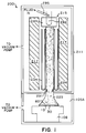
- Figure 1 is a cross-sectional schematic representation, partially in block form, of an apparatus that can be used in practicing the invention.
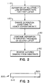
- Figure 2 is an operational flow diagram of a technique in accordance with an embodiment of the invention.
- Figure 3 is a cross-sectional representation of a diamond film made in accordance with an embodiment of the invention.
- FIG. 1 there is shown a diagram of a plasma jet deposition system 200 of a type which can be utilized in practicing an embodiment of the invention.
- the system 200 is contained within a housing 211 and includes an arc-forming section 215 which comprises a cylindrical cathode holder 294, a rod-like cathode 292, and an injector 295 mounted adjacent the cathode so as to permit injected fluid to pass over the cathode 292.
- a cylindrical anode is represented at 291.
- the input fluid may be a mixture of hydrogen and methane.
- the anode 291 and cathode 292 are energized by a source of electric potential (not shown), for example a DC potential.
- Cylindrical magnets are utilized to control the plasma generated at the arc forming section.
- the magnets maintain the plasma within a narrow column until the plasma reaches the deposition region 60.
- Optional cooling coils 234, in which a coolant can be circulated, can be located within the magnets.
- a mixture of hydrogen and methane is fed to the injector 295, and a plasma is obtained in front of the arc forming section and accelerated and focused toward the deposition region.
- the temperature and pressure at the plasma formation region are typically in the approximate ranges 1500-15,000 degrees C and 100-700 torr, respectively, and in the deposition region are in the approximate ranges 800-1100 degrees C and 0.1-200 torr, respectively.
- synthetic polycrystalline diamond can be formed from the described plasma, as the carbon in the methane is selectively deposited as diamond, and the graphite which forms is dissipated by combination with the hydrogen facilitating gas.
- U.S. Patent No.s 4,471,003, 4,487,162, and 5,204,144 For further description of plasma jet deposition systems, reference can be made to U.S. Patent No.s 4,471,003, 4,487,162, and 5,204,144. It will be understood that other suitable types of deposition equipment, including other types of CVD deposition equipment, can be used in conjunction with the features
- the bottom portion 105A of the chamber has a base 106 on which can be mounted a substrate 10 on which the synthetic diamond is to be deposited.
- the base can include a temperature controller.
- the substrate may be, for example, molybdenum, tungsten, or graphite, with molybdenum (and its alloys such as TZM, which contains relatively small percentages of titanium and zirconium) being presently-preferred.
- Molybdenum and its alloys such as TZM, which contains relatively small percentages of titanium and zirconium
- FIG 2 illustrates a titanium nitride interlayer, for coating the substrate on which the synthetic diamond is to be deposited and ultimately released.
- the substrate can be tilted and rotated during deposition as described, for example, in U.S. Patent No. 5,204,144.
- the block 110 represents the deposition, at a relatively low deposition rate, of a specified thickness of diamond film.
- the surface area deposited is at least 1000 square millimeters, but may be much larger.
- deposition covers the surface of a 4 inch diameter disc which is tilted and rotated during deposition.
- the thickness of the initial layer is at least 150 microns.
- the block 120 represents changing the deposition conditions to deposit diamond at higher deposition rate (permitting a higher level of defects in the diamond).
- this layer will be of lower quality than the initial layer, it is still fairly good quality synthetic diamond that has a relatively high thermal conductivity and may be employed, for example, in heat sinking applications.
- the second deposition rate for this example is at a deposition rate of about 11 ⁇ m/hr.
- the deposition conditions may be, for example, the same as listed above, but with the methane concentration at about .12 percent. Deposition under these conditions is continued (block 130), in this example, for about 78 hours, until the second layer thickness is at least about 850 microns. In the present example, the total film thickness is just over 1000 microns (1 mm). The thermal conductivity of even the higher growth rate material is still quite good, being approximately 10 W/cm °K.
- the layered diamond structure can then be released from the substrate, such as by cooling (see above-referenced copending U.S. Patent Application Serial No. 973,994), and removed from the deposition chamber, as represented by the block 150.
- Figure 3 illustrates the diamond film structure 300 of the above example, with the substrate side layer being represented at 310, and the deposition side layer at 320.
- nucleation density was controlled by varying the time at which the carbonaceous feedstock gas (in this case, methane) is introduced into the plasma, which is initially argon and hydrogen, during the substrate heating phase. In general, the earlier the methane is introduced, the higher the nucleation rate. After deposition, nucleation density was measured as the number of crystal grains per square millimeter of surface area, as determined using a scanning electron microscope on the nucleation side of the sample disc. The samples produced had so-called "flashing" which is the periphery of the sample that overlaps the edges of the circular mandrel and forms a rough annular rim.
- Bow was measured with an optical profilometer, and measured from the low point of the cupped surface to the plane defined by the highest points on the diamond sample periphery.
- Bow as measured, and as referred to herein, is measured after release and cooling to room temperature, and includes any component of bow resulting from mandrel distortion which is caused such as by the thermal gradient across the mandrel thickness.
- Mandrel distortion in the examples hereof was estimated to be about 40 microns.
- two synthetic diamond discs of thicknesses greater than 1000 microns were made at a deposition rate of about 11.7 microns per hour.
- One such disc was about 1,054 microns thick, had a measured nucleation density of about 1.6x10⁵ per mm2, and a measured bow of about 150 microns.
- the other disc was about 1070 microns thick, had a measured nucleation density of greater than 107 per mm2, and a measured bow of about 130 microns.
- bowing of the released diamond is with the deposition side curving to a convex shape.
- a synthetic diamond disc was made at a much lower deposition rate of about 4.8 microns per hour.
- the disc was about 1330 microns thick, had a measured nucleation density of about 1.6x10⁵ per mm2, and a measured bow of about 50 microns.
- it was determined that diamond deposited at a relatively low deposition rate (4.8 microns per hour being an example of a relatively low deposition rate for the equipment, parameters, and geometries hereof) did not exhibit problematic bowing.
- diamond disc samples were made in layers, with the initial (first) deposition rate being relatively low and the second deposition rate being relatively high.
- the thickness of the first layer for these samples was about 120 microns.
- the resultant diamond disc was about 1040 microns thick, had a measured nucleation density of about 1.4x10⁶, and a measured bow of about 149 microns.
- the resultant diamond disc was about 1040 microns thick, had a measured nucleation density of about 4x10⁴, and a measured bow of about 120 microns. It was seen from this and similar examples that, for the sample size and thickness involved, the 120 microns of initial relatively low defect (from relatively low deposition rate) layer is insufficient to prevent unacceptable bowing of the ultimate sample.
- samples were again made in layers, with an initial low deposition rate.
- the thickness of the first layer for these samples was about 380 microns.
- Several samples were made, with thicknesses varying between about 1230 microns and 1490 microns.
- the lower deposition rate for these samples was about 4.8 microns per hour, and the higher deposition rate was about 11.6 microns per hour.
- Nucleation density was about 4.9x10⁵ per mm2 for one sample, and greater than 107 per mm2 for most of the other samples.
- the measured bow was less than 100 microns, with the measured bow ranging from about 50 microns to about 99 microns, and averaging about 64 microns. It was seen from this and similar examples that, for the sample size and thickness involved, the 380 microns of initial relatively low defect layer is sufficient (and probably more than sufficient) to prevent unacceptable bowing of the ultimate sample.
- samples were again made in layers, with an initial low deposition rate.
- the thickness of the first layer for these samples was about 180 microns.
- Two samples were made, with thicknesses of about 1180 microns and 1270 microns.
- the lower deposition rate for these samples was about 4.8 microns per hour, and the higher deposition rate was about 11.6 microns per hour.
- Nucleation density for both was greater than 107 per mm2.
- the measured bow was less than 100 microns, with the measured bow for the 1180 micron thick sample being about 48 microns, and the measured bow for the 1270 micron thick sample being about 89 microns.
- the 180 microns of initial relatively low defect layer is sufficient to prevent unacceptable bowing of the ultimate sample.
- 120 microns is insufficient.
- a thickness of 150 microns is considered just sufficient.
Landscapes
- Chemical & Material Sciences (AREA)
- General Chemical & Material Sciences (AREA)
- Chemical Kinetics & Catalysis (AREA)
- Engineering & Computer Science (AREA)
- Materials Engineering (AREA)
- Mechanical Engineering (AREA)
- Metallurgy (AREA)
- Organic Chemistry (AREA)
- Inorganic Chemistry (AREA)
- Chemical Vapour Deposition (AREA)
- Crystals, And After-Treatments Of Crystals (AREA)
Applications Claiming Priority (2)
| Application Number | Priority Date | Filing Date | Title |
|---|---|---|---|
| US08/234,818 US5507987A (en) | 1994-04-28 | 1994-04-28 | Method of making a free-standing diamond film with reduced bowing |
| US234818 | 2002-09-04 |
Publications (2)
| Publication Number | Publication Date |
|---|---|
| EP0679732A1 true EP0679732A1 (fr) | 1995-11-02 |
| EP0679732B1 EP0679732B1 (fr) | 1998-09-23 |
Family
ID=22882955
Family Applications (1)
| Application Number | Title | Priority Date | Filing Date |
|---|---|---|---|
| EP95200915A Expired - Lifetime EP0679732B1 (fr) | 1994-04-28 | 1995-04-11 | Couche en diamant synthétique à flexion permanente réduite et procédé pour sa fabrication |
Country Status (5)
| Country | Link |
|---|---|
| US (2) | US5507987A (fr) |
| EP (1) | EP0679732B1 (fr) |
| JP (1) | JP3554074B2 (fr) |
| CA (1) | CA2144924A1 (fr) |
| DE (1) | DE69504896T2 (fr) |
Cited By (1)
| Publication number | Priority date | Publication date | Assignee | Title |
|---|---|---|---|---|
| EP0935012A3 (fr) * | 1998-02-05 | 2001-01-31 | Cvd Incorporated | Procédé de préparation de sulfure de zinc |
Families Citing this family (22)
| Publication number | Priority date | Publication date | Assignee | Title |
|---|---|---|---|---|
| US5474816A (en) * | 1993-04-16 | 1995-12-12 | The Regents Of The University Of California | Fabrication of amorphous diamond films |
| US6063149A (en) * | 1995-02-24 | 2000-05-16 | Zimmer; Jerry W. | Graded grain size diamond layer |
| US5663854A (en) * | 1995-06-07 | 1997-09-02 | International Business Machines Corporation | Prebent ceramic suspension |
| US5859105A (en) * | 1997-02-11 | 1999-01-12 | Johnson Matthey, Inc. | Organosilicon-containing compositions capable of rapid curing at low temperature |
| ATE353270T1 (de) * | 1998-07-31 | 2007-02-15 | Saint Gobain Abrasives Inc | Drehende abrichtrolle enthaltende abschleifende einsätze |
| KR100352985B1 (ko) | 1999-04-30 | 2002-09-18 | 한국과학기술연구원 | 균열이 없고 평탄한 다이아몬드막 합성 방법 |
| US6447891B1 (en) | 1999-05-03 | 2002-09-10 | Guardian Industries Corp. | Low-E coating system including protective DLC |
| US6475573B1 (en) | 1999-05-03 | 2002-11-05 | Guardian Industries Corp. | Method of depositing DLC inclusive coating on substrate |
| US6261693B1 (en) | 1999-05-03 | 2001-07-17 | Guardian Industries Corporation | Highly tetrahedral amorphous carbon coating on glass |
| US6280834B1 (en) | 1999-05-03 | 2001-08-28 | Guardian Industries Corporation | Hydrophobic coating including DLC and/or FAS on substrate |
| US6312808B1 (en) | 1999-05-03 | 2001-11-06 | Guardian Industries Corporation | Hydrophobic coating with DLC & FAS on substrate |
| US6277480B1 (en) | 1999-05-03 | 2001-08-21 | Guardian Industries Corporation | Coated article including a DLC inclusive layer(s) and a layer(s) deposited using siloxane gas, and corresponding method |
| US6368664B1 (en) | 1999-05-03 | 2002-04-09 | Guardian Industries Corp. | Method of ion beam milling substrate prior to depositing diamond like carbon layer thereon |
| US6335086B1 (en) | 1999-05-03 | 2002-01-01 | Guardian Industries Corporation | Hydrophobic coating including DLC on substrate |
| US6461731B1 (en) | 1999-05-03 | 2002-10-08 | Guardian Industries Corp. | Solar management coating system including protective DLC |
| GB2366804B (en) * | 2000-09-19 | 2003-04-09 | Kinik Co | Cast diamond tools and their formation by chemical vapor deposition |
| WO2007084501A2 (fr) * | 2006-01-13 | 2007-07-26 | Group4 Labs, Llc | Procede destine a la fabrication de dissipateurs thermiques a base de diamant lisse |
| US10258959B2 (en) | 2010-08-11 | 2019-04-16 | Unit Cell Diamond Llc | Methods of producing heterodiamond and apparatus therefor |
| US9783885B2 (en) | 2010-08-11 | 2017-10-10 | Unit Cell Diamond Llc | Methods for producing diamond mass and apparatus therefor |
| US9469918B2 (en) | 2014-01-24 | 2016-10-18 | Ii-Vi Incorporated | Substrate including a diamond layer and a composite layer of diamond and silicon carbide, and, optionally, silicon |
| JP6450919B2 (ja) * | 2014-02-05 | 2019-01-16 | アダマンド並木精密宝石株式会社 | ダイヤモンド基板及びダイヤモンド基板の製造方法 |
| DE102022205081A1 (de) | 2022-05-20 | 2023-11-23 | Universität Augsburg, Körperschaft des öffentlichen Rechts | Verfahren, Substrat, Vorrichtung und deren Verwendung zur Synthese von ebenen einkristallinen Diamanten |
Citations (4)
| Publication number | Priority date | Publication date | Assignee | Title |
|---|---|---|---|---|
| EP0467043A2 (fr) * | 1990-06-13 | 1992-01-22 | General Electric Company | Feuille de diamant autoportante, méthode et appareillage pour sa fabrication |
| US5110579A (en) * | 1989-09-14 | 1992-05-05 | General Electric Company | Transparent diamond films and method for making |
| US5124179A (en) * | 1990-09-13 | 1992-06-23 | Diamonex, Incorporated | Interrupted method for producing multilayered polycrystalline diamond films |
| US5270077A (en) * | 1991-12-13 | 1993-12-14 | General Electric Company | Method for producing flat CVD diamond film |
Family Cites Families (21)
| Publication number | Priority date | Publication date | Assignee | Title |
|---|---|---|---|---|
| US4471003A (en) * | 1980-11-25 | 1984-09-11 | Cann Gordon L | Magnetoplasmadynamic apparatus and process for the separation and deposition of materials |
| US4487162A (en) * | 1980-11-25 | 1984-12-11 | Cann Gordon L | Magnetoplasmadynamic apparatus for the separation and deposition of materials |
| SE442305B (sv) * | 1984-06-27 | 1985-12-16 | Santrade Ltd | Forfarande for kemisk gasutfellning (cvd) for framstellning av en diamantbelagd sammansatt kropp samt anvendning av kroppen |
| US4900628A (en) * | 1986-07-23 | 1990-02-13 | Sumitomo Electric Industries, Ltd. | Gaseous phase synthesized diamond and method for synthesizing same |
| JP2603257B2 (ja) * | 1987-06-05 | 1997-04-23 | 株式会社神戸製鋼所 | ダイヤモンド多層薄膜 |
| US5131963A (en) * | 1987-11-16 | 1992-07-21 | Crystallume | Silicon on insulator semiconductor composition containing thin synthetic diamone films |
| US5006703A (en) * | 1988-02-22 | 1991-04-09 | Victor Company Of Japan, Ltd. | Reflective optical rotary encoder disc |
| JPH0757039B2 (ja) * | 1988-05-09 | 1995-06-14 | 株式会社ケンウッド | 音響用振動板及びその製造法 |
| US5006203A (en) * | 1988-08-12 | 1991-04-09 | Texas Instruments Incorporated | Diamond growth method |
| US4988421A (en) * | 1989-01-12 | 1991-01-29 | Ford Motor Company | Method of toughening diamond coated tools |
| GB8912498D0 (en) * | 1989-05-31 | 1989-07-19 | De Beers Ind Diamond | Diamond growth |
| CA2034440A1 (fr) * | 1990-02-13 | 1991-08-14 | Thomas R. Anthony | Pieces diamantees par dcpv et methode de fabrication |
| DE69112465T2 (de) * | 1990-03-30 | 1996-03-28 | Sumitomo Electric Industries | Polykristallines Diamantwerkzeug und Verfahren für seine Herstellung. |
| US5126207A (en) * | 1990-07-20 | 1992-06-30 | Norton Company | Diamond having multiple coatings and methods for their manufacture |
| US5260106A (en) * | 1990-08-03 | 1993-11-09 | Fujitsu Limited | Method for forming diamond films by plasma jet CVD |
| US5310512A (en) * | 1990-11-15 | 1994-05-10 | Norton Company | Method for producing synthetic diamond structures |
| JP3028660B2 (ja) * | 1991-10-21 | 2000-04-04 | 住友電気工業株式会社 | ダイヤモンドヒートシンクの製造方法 |
| US5204144A (en) * | 1991-05-10 | 1993-04-20 | Celestech, Inc. | Method for plasma deposition on apertured substrates |
| US5183689A (en) * | 1991-07-15 | 1993-02-02 | Cvd, Inc. | Process for an improved laminated of znse and zns |
| US5314652A (en) * | 1992-11-10 | 1994-05-24 | Norton Company | Method for making free-standing diamond film |
| US5272104A (en) * | 1993-03-11 | 1993-12-21 | Harris Corporation | Bonded wafer process incorporating diamond insulator |
-
1994
- 1994-04-28 US US08/234,818 patent/US5507987A/en not_active Expired - Fee Related
-
1995
- 1995-03-17 CA CA002144924A patent/CA2144924A1/fr not_active Abandoned
- 1995-04-11 EP EP95200915A patent/EP0679732B1/fr not_active Expired - Lifetime
- 1995-04-11 DE DE69504896T patent/DE69504896T2/de not_active Expired - Fee Related
- 1995-04-28 JP JP10644795A patent/JP3554074B2/ja not_active Expired - Fee Related
- 1995-05-31 US US08/456,169 patent/US5679446A/en not_active Expired - Fee Related
Patent Citations (4)
| Publication number | Priority date | Publication date | Assignee | Title |
|---|---|---|---|---|
| US5110579A (en) * | 1989-09-14 | 1992-05-05 | General Electric Company | Transparent diamond films and method for making |
| EP0467043A2 (fr) * | 1990-06-13 | 1992-01-22 | General Electric Company | Feuille de diamant autoportante, méthode et appareillage pour sa fabrication |
| US5124179A (en) * | 1990-09-13 | 1992-06-23 | Diamonex, Incorporated | Interrupted method for producing multilayered polycrystalline diamond films |
| US5270077A (en) * | 1991-12-13 | 1993-12-14 | General Electric Company | Method for producing flat CVD diamond film |
Cited By (1)
| Publication number | Priority date | Publication date | Assignee | Title |
|---|---|---|---|---|
| EP0935012A3 (fr) * | 1998-02-05 | 2001-01-31 | Cvd Incorporated | Procédé de préparation de sulfure de zinc |
Also Published As
| Publication number | Publication date |
|---|---|
| EP0679732B1 (fr) | 1998-09-23 |
| DE69504896D1 (de) | 1998-10-29 |
| DE69504896T2 (de) | 1999-06-10 |
| CA2144924A1 (fr) | 1995-10-29 |
| US5507987A (en) | 1996-04-16 |
| JPH0881299A (ja) | 1996-03-26 |
| JP3554074B2 (ja) | 2004-08-11 |
| US5679446A (en) | 1997-10-21 |
Similar Documents
| Publication | Publication Date | Title |
|---|---|---|
| EP0679732B1 (fr) | Couche en diamant synthétique à flexion permanente réduite et procédé pour sa fabrication | |
| US5314652A (en) | Method for making free-standing diamond film | |
| EP0693573B1 (fr) | Production d'un film diamant | |
| EP0752293B1 (fr) | Article revêtu de diamant et son procédé de préparation | |
| US5518766A (en) | Multi-layer superhard film structure | |
| AU736551B2 (en) | A method of coating edges with diamond-like carbon | |
| EP0695816B1 (fr) | Procédé pour la fabrication d'une couche de diamant à flexion réduite | |
| CA2204086C (fr) | Production de film en diamant | |
| EP1640482A1 (fr) | Procede de production d'un film mince de diamant microcristallin extremement plat au moyen d'un procede d'ablation laser | |
| EP0556615B1 (fr) | Méthode pour la fabrication de diamants synthétiques | |
| EP0807693B1 (fr) | Elément d'usure en diamant synthétique et procédé de fabrication | |
| JPH075304A (ja) | ダイヤモンドをコーティングした構造体の製造方法 | |
| Lee et al. | Enhanced nucleation density of chemical vapor deposition diamonds by using interlayer | |
| KR100484263B1 (ko) | 절삭공구에서 미세결정다이아몬드 특성을 가진 코팅막의형성방법 | |
| JPH0623431B2 (ja) | 硬質被膜被覆切削工具部材 | |
| JPH06262406A (ja) | 切削工具およびその製造法 | |
| JPH04108690A (ja) | ダイヤモンドの合成方法 | |
| JPH069292A (ja) | ダイヤモンド厚膜の製造法およびダイヤモンド厚膜をろう付けして得られたダイヤモンド切削工具 |
Legal Events
| Date | Code | Title | Description |
|---|---|---|---|
| PUAI | Public reference made under article 153(3) epc to a published international application that has entered the european phase |
Free format text: ORIGINAL CODE: 0009012 |
|
| AK | Designated contracting states |
Kind code of ref document: A1 Designated state(s): DE FR GB |
|
| 17P | Request for examination filed |
Effective date: 19960502 |
|
| 17Q | First examination report despatched |
Effective date: 19970425 |
|
| GRAG | Despatch of communication of intention to grant |
Free format text: ORIGINAL CODE: EPIDOS AGRA |
|
| GRAG | Despatch of communication of intention to grant |
Free format text: ORIGINAL CODE: EPIDOS AGRA |
|
| GRAH | Despatch of communication of intention to grant a patent |
Free format text: ORIGINAL CODE: EPIDOS IGRA |
|
| RAP1 | Party data changed (applicant data changed or rights of an application transferred) |
Owner name: SAINT-GOBAIN INDUSTRIAL CERAMICS, INC. |
|
| GRAH | Despatch of communication of intention to grant a patent |
Free format text: ORIGINAL CODE: EPIDOS IGRA |
|
| GRAA | (expected) grant |
Free format text: ORIGINAL CODE: 0009210 |
|
| AK | Designated contracting states |
Kind code of ref document: B1 Designated state(s): DE FR GB |
|
| REF | Corresponds to: |
Ref document number: 69504896 Country of ref document: DE Date of ref document: 19981029 |
|
| ET | Fr: translation filed | ||
| PLBE | No opposition filed within time limit |
Free format text: ORIGINAL CODE: 0009261 |
|
| STAA | Information on the status of an ep patent application or granted ep patent |
Free format text: STATUS: NO OPPOSITION FILED WITHIN TIME LIMIT |
|
| 26N | No opposition filed | ||
| REG | Reference to a national code |
Ref country code: GB Ref legal event code: IF02 |
|
| PGFP | Annual fee paid to national office [announced via postgrant information from national office to epo] |
Ref country code: GB Payment date: 20040407 Year of fee payment: 10 |
|
| PGFP | Annual fee paid to national office [announced via postgrant information from national office to epo] |
Ref country code: FR Payment date: 20040420 Year of fee payment: 10 |
|
| PGFP | Annual fee paid to national office [announced via postgrant information from national office to epo] |
Ref country code: DE Payment date: 20040601 Year of fee payment: 10 |
|
| PG25 | Lapsed in a contracting state [announced via postgrant information from national office to epo] |
Ref country code: GB Free format text: LAPSE BECAUSE OF NON-PAYMENT OF DUE FEES Effective date: 20050411 |
|
| PG25 | Lapsed in a contracting state [announced via postgrant information from national office to epo] |
Ref country code: DE Free format text: LAPSE BECAUSE OF NON-PAYMENT OF DUE FEES Effective date: 20051101 |
|
| GBPC | Gb: european patent ceased through non-payment of renewal fee |
Effective date: 20050411 |
|
| PG25 | Lapsed in a contracting state [announced via postgrant information from national office to epo] |
Ref country code: FR Free format text: LAPSE BECAUSE OF NON-PAYMENT OF DUE FEES Effective date: 20051230 |
|
| REG | Reference to a national code |
Ref country code: FR Ref legal event code: ST Effective date: 20051230 |