EP0680070A1 - Appareil et méthode de traitement de substrats - Google Patents
Appareil et méthode de traitement de substrats Download PDFInfo
- Publication number
- EP0680070A1 EP0680070A1 EP95110162A EP95110162A EP0680070A1 EP 0680070 A1 EP0680070 A1 EP 0680070A1 EP 95110162 A EP95110162 A EP 95110162A EP 95110162 A EP95110162 A EP 95110162A EP 0680070 A1 EP0680070 A1 EP 0680070A1
- Authority
- EP
- European Patent Office
- Prior art keywords
- section
- substrate
- plasma
- treating
- substrates
- Prior art date
- Legal status (The legal status is an assumption and is not a legal conclusion. Google has not performed a legal analysis and makes no representation as to the accuracy of the status listed.)
- Withdrawn
Links
Images


Classifications
-
- H—ELECTRICITY
- H01—ELECTRIC ELEMENTS
- H01J—ELECTRIC DISCHARGE TUBES OR DISCHARGE LAMPS
- H01J37/00—Discharge tubes with provision for introducing objects or material to be exposed to the discharge, e.g. for the purpose of examination or processing thereof
- H01J37/32—Gas-filled discharge tubes
- H01J37/32009—Arrangements for generation of plasma specially adapted for examination or treatment of objects, e.g. plasma sources
- H01J37/32082—Radio frequency generated discharge
- H01J37/32091—Radio frequency generated discharge the radio frequency energy being capacitively coupled to the plasma
-
- H—ELECTRICITY
- H10—SEMICONDUCTOR DEVICES; ELECTRIC SOLID-STATE DEVICES NOT OTHERWISE PROVIDED FOR
- H10P—GENERIC PROCESSES OR APPARATUS FOR THE MANUFACTURE OR TREATMENT OF DEVICES COVERED BY CLASS H10
- H10P50/00—Etching of wafers, substrates or parts of devices
-
- H—ELECTRICITY
- H01—ELECTRIC ELEMENTS
- H01J—ELECTRIC DISCHARGE TUBES OR DISCHARGE LAMPS
- H01J37/00—Discharge tubes with provision for introducing objects or material to be exposed to the discharge, e.g. for the purpose of examination or processing thereof
- H01J37/32—Gas-filled discharge tubes
- H01J37/32009—Arrangements for generation of plasma specially adapted for examination or treatment of objects, e.g. plasma sources
- H01J37/32357—Generation remote from the workpiece, e.g. down-stream
-
- H—ELECTRICITY
- H01—ELECTRIC ELEMENTS
- H01J—ELECTRIC DISCHARGE TUBES OR DISCHARGE LAMPS
- H01J37/00—Discharge tubes with provision for introducing objects or material to be exposed to the discharge, e.g. for the purpose of examination or processing thereof
- H01J37/32—Gas-filled discharge tubes
- H01J37/32431—Constructional details of the reactor
- H01J37/32623—Mechanical discharge control means
-
- H—ELECTRICITY
- H10—SEMICONDUCTOR DEVICES; ELECTRIC SOLID-STATE DEVICES NOT OTHERWISE PROVIDED FOR
- H10P—GENERIC PROCESSES OR APPARATUS FOR THE MANUFACTURE OR TREATMENT OF DEVICES COVERED BY CLASS H10
- H10P50/00—Etching of wafers, substrates or parts of devices
- H10P50/20—Dry etching; Plasma etching; Reactive-ion etching
- H10P50/28—Dry etching; Plasma etching; Reactive-ion etching of insulating materials
- H10P50/282—Dry etching; Plasma etching; Reactive-ion etching of insulating materials of inorganic materials
- H10P50/283—Dry etching; Plasma etching; Reactive-ion etching of insulating materials of inorganic materials by chemical means
-
- H—ELECTRICITY
- H01—ELECTRIC ELEMENTS
- H01J—ELECTRIC DISCHARGE TUBES OR DISCHARGE LAMPS
- H01J2237/00—Discharge tubes exposing object to beam, e.g. for analysis treatment, etching, imaging
- H01J2237/32—Processing objects by plasma generation
- H01J2237/33—Processing objects by plasma generation characterised by the type of processing
- H01J2237/334—Etching
- H01J2237/3343—Problems associated with etching
- H01J2237/3345—Problems associated with etching anisotropy
-
- H—ELECTRICITY
- H01—ELECTRIC ELEMENTS
- H01J—ELECTRIC DISCHARGE TUBES OR DISCHARGE LAMPS
- H01J2237/00—Discharge tubes exposing object to beam, e.g. for analysis treatment, etching, imaging
- H01J2237/32—Processing objects by plasma generation
- H01J2237/33—Processing objects by plasma generation characterised by the type of processing
- H01J2237/334—Etching
- H01J2237/3343—Problems associated with etching
- H01J2237/3348—Problems associated with etching control of ion bombardment energy
Definitions
- the present invention relates to an apparatus for etching and ashing substrates such as semiconductor wafers. It also relates to a method of doing the same.
- a micro-pattern of an integrated circuit on a semiconductor is formed by etching an undercoat film on the semiconductor wafer while using an organic high polymer photo-resist film as its mask.
- the photo-resist film is removed from the surface of the semiconductor wafer after this etching process.
- a plasma etching apparatus having an independent unit chamber to the etching process has been used as one of the substrate treating apparatuses.
- An ashing apparatus having an independent unit chamber to the ashing process has also been used as one of the substrate treating apparatuses.
- a sequence treating apparatus which is a combination of plural treatment units to achieve various functions is now in use.
- the anisotropic etching is carried out in a main chamber, the isotropic etching (or light etching for removing damage portion of the silicon film) is then carried out in an after-treatment chamber and the ashing is finally carried out in an ashing chamber.
- the wafers are usually treated one by one.
- the anisotropic etching step, isotropic etching step and the ashing step must be carried out by their corresponding apparatuses and the wafers to be treated must be carried between these apparatuses by hands or by automatic carriage means. This makes it necessary to carry the wafers between these apparatuses and carry them into and out of these apparatuses, thereby making low the throughput to put together the all processes.
- the wafers are contacted with atmosphere while being carried between these apparatuses. This allows dust, impurities and water in atmosphere to adhere to the wafers, thereby creating fault patterns and making the revival of treatment worse. Further, the floor space occupied by the system is increased.
- An object of the present invention is therefore to provide an apparatus for treating substrates and also to provide a method for doing the same, said apparatus and method being capable of making the treatment speed higher, increasing the throughput, reducing the floor space occupied by the system, and preventing the substrates such as semiconductor wafers from being contaminated by atmosphere.
- a substrates treating apparatus comprising a chamber provided with a section at which the substrates are treated and with another section at which plasma is generated, means for supplying gas into the plasma generating section, electrode means for changing the gas into plasma in the plasma generating section, an ion trap means arranged between the plasma generating section and the substrates treating section to trap ions in the plasma so as to allow neutral radicals to be introduced into the substrates treating section, and means for exhausting the substrates treating section.
- a substrates treating method comprising preparing the substrate at a substrates treating section in a chamber, introducing gas into a plasma generating section in the chamber, changing the gas into plasma in the plasma generating section, taking out neutral radicals from the plasma, and acting the neutral radicals on the substrate in the substrates treating section.
- the inner diameter of the plasma generating section is made smaller than that of the substrates processing section.
- the interval between the electrodes is thus made small to generate plasma of high density.
- the inner diameter of the plasma generating section is in a range of 20 - 60mm.
- a substrate mount is provided with a lifter means to change the interval between the substrate and the ion trap. In this manner it is possible to control the ratio of fluorine radicals allowed to reach the substrate, which are long in life, to oxyger radicals allowed to reach the substrate, which are short in life.
- a substrates treating apparatus of the present invention plasma of high density can be generated and introduced into the substrates treating section through the ion trap to act on the substrate to be treated. Therefore, only radicals are allowed to act on the substrate to be treated, so that the isotropic etching can be carried out at a higher rate without damaging the substrate by ions. Even when the substrates are treated one by one, for example, a throughput in the anisotropic etching can be achieved substantially same in the isotropic etching.
- the substrates treating section can be connected to a section in which the anisotropic etching apparatus is housed, to thereby treat the substrates one by one while keeping them not contacted with atmosphere.
- process gas can be a mixture of ashing and etching gases
- the ashing and isotropic etching processes can be carried out at the same time, and the rate of the ashing speed relative to the' etching speed can be controlled to a desired value by adjusting at least one of alternative current, the pressure and flow rate of gas and the rate of gases mixed.
- the ashing and isotropic etching processes can be therefore carried out in a same chamber to thereby make the throughput higher.
- the floor space occupied by the system can be reduced because the number of apparatuses used is reduced.
- a system 10 for etching and ashing semiconductor wafers comprises plural chamber units 11 - 15.
- a main chamber (MC) 12 is located between load lock chambers (LLC) 11 and 13 and an after-treatment chamber (ATC) 14 between load lock chambers 13 and 15.
- LLC load lock chambers
- ATC after-treatment chamber
- Each of the load lock chambers 11, 13 and 15 is provided with a handling device (not shown), by which semiconductor wafers can be carried one by one into and out of the chamber through a gate section (not shown).
- a cassette conveying passage (not shown) is arranged adjacent to a front gate of the first load lock chamber 11.
- a carriage robot (not shown) runs on the cassette conveying passage to convey wafer cassettes from a developing section (not shown) to a cassette station (not shown).
- the cassette station is located in front of the front gate of the first load lock chamber 11.
- a cassette station (not shown) is located adjacent to a rear gate of the third load lock chamber 15.
- Exhaust and nitrogen gas supply pipes (not shown) are passed through a wall of the load lock chambers 11, 13 and 15, respectively.
- a pair of plate electrodes (not shown) parallel to each other are arranged in the main chamber 12 and a Si film on the wafer is anisotropy-etched by plasma generated between the electrodes.
- Exhaust pipe (not shown) and process gas supply pipe (not shown) are passed through a wall of the main chamber 12.
- the after-treatment chamber (ATC) 14 will be described referring to Fig. 2.
- a wafer mount 23 which can hold a semiconductor wafer 2 thereon by an electrostatic chuck device, for example, is arranged in the ATC 14.
- This wafer mount 23 is housed in a treating section 24 which is shaped like a hollow cylinder having a diameter of 200 mm, for example.
- the wafer mount 23 is moved up and down by a lifter means 22 and it is also provided with a heater (not shown).
- a plasma generating section 25 is located above the treating section 24, which is shaped like a hollow cylinder having a diameter smaller than that of the treating section 24.
- a cylindrical tube 26 made of quartz and having a diameter of 40 mm, for example, smaller than that of the treating section 24 is connected to upper portion of the treating section 24.
- a pair of electrodes 28a and 28b are wound round the quartz-made cylindrical tube 26 with an insulating spacer 27 interposed between them.
- One 28a of these electrodes is connected to a high frequency power source 30 via a matching circuit 29 while the other 28b is grounded.
- a gas supply pipe 31 is connected to the upper end of the cylindrical tube 26 and it is also connected to process gas supply sources (GSS) 32a and 32b through mass flow controllers (MFC) 33a and 33b.
- Oxygen gas is contained in the first GSS 32a and CF4 gas in the second GSS 32b.
- An exhaust pipe 35 of an exhaust device 34 is connected to the lower portion of the treating section 24.
- Gate devices 36 and 37 are arranged on both sides of the treating section 24 to allow the semiconductor wafer 2 to be carried into and out of the treating section 24.
- the ATC 14 is partitioned from the second and third load lock chambers 13 and 15 by these gate devices 36 and 37.
- an ion trap 38 is provided between the treating section 24 and the plasma generating section 25.
- This ion trap 38 is made by forming a plurality of holes 38b (each having a diameter of 0.2 - 0.5 mm, for example) in a conductive aluminium plate 38a, for example, and it is earthed. Ions in plasma generated at the plasma generating section 25 are caught by the ion trap 38 so as to allow only those radicals which are electrically neutral to act on the semiconductor wafer 2.
- the ion trap 38 may be a mesh-like electrode.
- a controller 21 backed up by a computer 20 is connected to power source switches for the means of the ATC 14. Namely, it is arranged that command signal is sent from the controller 21 to the high frequency power source 30, GSS 32a, 32b, MFC 33a, 33b, lifter device 22, exhaust device 34, gate device 36, 37, electrostatic chuck device, heating device for heating the wafer mount 23 and a wafer handling device (not shown).
- the silicon wafer 2 which has been coated with a photo-resist and then developed is taken out from the cassette and carried into the first load lock chamber 11 by the handling device (step 51).
- the first load lock chamber 11 is closed by its front gate and then exhausted.
- the rear gate of the first load lock chamber 11 is opened to communicate the first load lock chamber 11 with the main chamber 12.
- the wafer 2 is carried from the first load lock chamber 11 into the main chamber 12 (step 52).
- Anisotropic etching is applied to the wafer 2 in the main chamber 12 (step 53).
- a layer 2b of SiO2 on the wafer 2 is thus partially removed.
- Reference numeral 2a represents the layer of silicon and 2c the layer of photo-resist. That area 3 on the surface of the silicon layer 2a from which the SiO2 layer has been removed by the anisotropic etching is damaged as shown in Fig. 4B.
- the rear gate of the main chamber 12 is then opened and the wafer 2 is carried from the main chamber 12 into the second load lock chamber 13 by the handling device (step 54).
- the rear gate is closed and the load lock chamber 13 is exhausted until the internal pressure of the second load lock chamber 13 becomes substantially same as that of the ATC 14.
- the front gate 36 of the ATC 14 is opened and the wafer 2 is carried from the load lock chamber 13 into the ATC 14 by the handling device (step 55).
- the wafer 2 is fixed on the wafer mount 23 by the electrostatic chuck device.
- the wafer mount 23 is previously heated to a predetermined temperature or about 50°C, for example.
- the wafer mount 23 is lifted by the lifter device 22 and the interval L between the ion trap 38 and the semiconductor wafer 2 is set a predetermined value of 10 - 50 mm, for example, where most ion radicals are present.
- predetermined process gas such as (O2 + CF4) mixed gas is introduced from the gas supply sources 32a and 32b into the plasma generating section 25.
- current having a predetermined high frequency of 1356MHz, for example, is supplied from the high frequency power source 30 to the electrodes 28a and 28b through the matching circuit 29.
- Plasma of high density is thus generated in the plasma generating section 25 smaller in diameter than the treating section 24 and this plasma gas is diffused as shown by arrows in Fig. 2. Ions in the plasma gas are removed while it is passing through the ion trap 38, and radicals thus left are supplied to the semiconductor wafer 2 on the wafer mount 23 to conduct the anisotropic etching to the damaged area 3 of the silicon layer 2 and the ashing to the photo-resist layer 2c at the same time (step 56). In order to apply the anisotropic etching and the ashing to the semiconductor wafer 2 to desired extents in this case, it is necessary to control the rate of the etching and the ashing.
- the ratio of etching rate/ashing rate (which will be hereinafter referred to as VS. Poly) can be controlled by adjusting at least one of current added to the electrodes 28a and 28b, the gas flow rate, gas pressure and components of process gas and the interval L.
- the plasma When the plasma is passed through the holes 38b of the ion trap 38, ions are removed from it, thereby allowing oxygen radicals and fluorine radicals to reach the wafer 2 in the treating section 24.
- the oxygen radicals of them react with the photo-resist layer 2c on the wafer 2 to remove the photo-resist layer 2c from the wafer 2 (ashing).
- the fluorine radicals react with the silicon layer 2a on the wafer 2 to remove the damaged area 3 to a depth of 50 - 100 ⁇ (anisotropic etching).
- the oxygen radicals are usually shorter in life than the fluorine radicals.
- the interval L between the wafer 2 and the ion trap 38 is made too large, therefore, the oxygen radicals become to oxygen gas molecules, so that the photo-resist layer 2c cannot be removed from the wafer 2 because of oxidation reaction.
- the speed of anisotropic etching is increased not to set an appropriate light etching rate.
- the wafer 2 is then carried from the ATC 14 into the third load lock chamber 15 (step 57) and further carried out of the load lock chamber 15 (step 58).
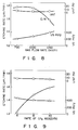
- etching rate (ER), an uniformity (Unif) and a ratio of etching rate/ashing rate (VS. Poly) are plotted on vertical axes of graphs shown in Figs. 6 through 9.
- alternative current is plotted on a horizontal axis of the graph shown in Fig. 6, the pressure of treating gas on a horizontal axis of the graph in Fig. 7, the flow rate of process gas on a horizontal axis of the graph in Fig. 8, and the rate of CF4 added to the process gas on a horizontal axis of the graph in Fig. 9.
- the total flow volume of CF4 and O2 mixed gas is 1250SCCM and except the case shown in Fig. 9, the ratio of process gas comprises O2 of 90% and CF4 of 10%.
- VS. Poly is selected to be 200 - 500.
- plasma is generated in the plasma generating section 25 which has a diameter smaller than that of the treating section 24 and it is introduced into the treating section 24 through the ion trap 38 to act on the semiconductor wafer 2 in the section 24. Therefore, it can be generated to have a higher density and it can also be generated at a higher efficiency.
- the ashing rate at the ashing process can be greater than that of the conventional case (about thirty times of the conventional case), and a throughput (one wafer per minute, for example) same as that at the anisotropic etching can be attained.
- ions in the plasma can be removed by the ion trap 38 to allow only radicals to be reacted with the semiconductor wafer 2. This enables the isotropic etching to be carried without damaging the semiconductor wafer 2.
- the isotropic etching relative to the silicon layer on the wafer 2 and the ashing relative to the photo-resist layer thereon can be carried out at the same time to thereby increase the throughput.
- the ashing device and the carriage means for carrying the wafer between the section at which the isotropic etching treatment is carried out and the section at which the ashing treatment is carried out are made unnecessary to thereby reduce the floor space occupied by the system. The space particularly in a clean room whose constructing cost is high can be more efficiently used.
- AC has been used as the plasma power source in the case of the above-described embodiment
- DC may be used.
- the treating speed can be made higher at the isotropic etching and ashing processes to thereby increase the throughput.
- the floor space occupied by the system can be reduced and treatments can be carried out while keeping the wafer not contacted with atmosphere.
Landscapes
- Physics & Mathematics (AREA)
- Engineering & Computer Science (AREA)
- Plasma & Fusion (AREA)
- Chemical & Material Sciences (AREA)
- Analytical Chemistry (AREA)
- Drying Of Semiconductors (AREA)
Applications Claiming Priority (3)
| Application Number | Priority Date | Filing Date | Title |
|---|---|---|---|
| JP335671/90 | 1990-11-30 | ||
| JP2335671A JP2888258B2 (ja) | 1990-11-30 | 1990-11-30 | 基板処理装置および基板処理方法 |
| EP91120577A EP0488393B1 (fr) | 1990-11-30 | 1991-11-29 | Méthode de traitement de substrats |
Related Parent Applications (1)
| Application Number | Title | Priority Date | Filing Date |
|---|---|---|---|
| EP91120577.1 Division | 1991-11-29 |
Publications (1)
| Publication Number | Publication Date |
|---|---|
| EP0680070A1 true EP0680070A1 (fr) | 1995-11-02 |
Family
ID=18291212
Family Applications (2)
| Application Number | Title | Priority Date | Filing Date |
|---|---|---|---|
| EP91120577A Expired - Lifetime EP0488393B1 (fr) | 1990-11-30 | 1991-11-29 | Méthode de traitement de substrats |
| EP95110162A Withdrawn EP0680070A1 (fr) | 1990-11-30 | 1991-11-29 | Appareil et méthode de traitement de substrats |
Family Applications Before (1)
| Application Number | Title | Priority Date | Filing Date |
|---|---|---|---|
| EP91120577A Expired - Lifetime EP0488393B1 (fr) | 1990-11-30 | 1991-11-29 | Méthode de traitement de substrats |
Country Status (6)
| Country | Link |
|---|---|
| US (1) | US5385624A (fr) |
| EP (2) | EP0488393B1 (fr) |
| JP (1) | JP2888258B2 (fr) |
| KR (1) | KR100238623B1 (fr) |
| DE (1) | DE69124672T2 (fr) |
| TW (1) | TW285745B (fr) |
Cited By (3)
| Publication number | Priority date | Publication date | Assignee | Title |
|---|---|---|---|---|
| WO1999034424A1 (fr) * | 1997-12-30 | 1999-07-08 | Applied Materials, Inc. | Etape de nettoyage preliminaire effectuee avant la metallisation destinee a une application d'une precision inferieure au quart de micron |
| WO2004074932A3 (fr) * | 2003-02-14 | 2004-10-21 | Applied Materials Inc | Nettoyage d'oxyde naturel au moyen de radicaux contenant de l'hydrogene |
| EP1355342A3 (fr) * | 2002-04-19 | 2006-05-17 | Nordson Corporation | Dispositif de traitement par plasma |
Families Citing this family (70)
| Publication number | Priority date | Publication date | Assignee | Title |
|---|---|---|---|---|
| JPH04253328A (ja) * | 1991-01-29 | 1992-09-09 | Hitachi Ltd | 表面処理装置 |
| DE4132558C1 (fr) * | 1991-09-30 | 1992-12-03 | Secon Halbleiterproduktionsgeraete Ges.M.B.H., Wien, At | |
| US5423936A (en) * | 1992-10-19 | 1995-06-13 | Hitachi, Ltd. | Plasma etching system |
| JPH06188229A (ja) * | 1992-12-16 | 1994-07-08 | Tokyo Electron Yamanashi Kk | エッチングの後処理方法 |
| US5578129A (en) * | 1993-03-17 | 1996-11-26 | Tokyo Electron Limited | Gas supplying head and load lock chamber of semiconductor processing system |
| JP3223661B2 (ja) * | 1993-08-31 | 2001-10-29 | ソニー株式会社 | プラズマ堆積方法 |
| US5783100A (en) * | 1994-03-16 | 1998-07-21 | Micron Display Technology, Inc. | Method of high density plasma etching for semiconductor manufacture |
| US5811022A (en) | 1994-11-15 | 1998-09-22 | Mattson Technology, Inc. | Inductive plasma reactor |
| US5571577A (en) * | 1995-04-07 | 1996-11-05 | Board Of Trustees Operating Michigan State University | Method and apparatus for plasma treatment of a surface |
| KR100275597B1 (ko) * | 1996-02-23 | 2000-12-15 | 나카네 히사시 | 플리즈마처리장치 |
| US6248206B1 (en) * | 1996-10-01 | 2001-06-19 | Applied Materials Inc. | Apparatus for sidewall profile control during an etch process |
| DE19734278C1 (de) * | 1997-08-07 | 1999-02-25 | Bosch Gmbh Robert | Vorrichtung zum anisotropen Ätzen von Substraten |
| JP3317209B2 (ja) * | 1997-08-12 | 2002-08-26 | 東京エレクトロンエイ・ティー株式会社 | プラズマ処理装置及びプラズマ処理方法 |
| US6049736A (en) * | 1997-09-03 | 2000-04-11 | Medtronic, Inc. | Implantable medical device with electrode lead having improved surface characteristics |
| US6399445B1 (en) * | 1997-12-18 | 2002-06-04 | Texas Instruments Incorporated | Fabrication technique for controlled incorporation of nitrogen in gate dielectric |
| US6013316A (en) | 1998-02-07 | 2000-01-11 | Odme | Disc master drying cover assembly |
| US6635578B1 (en) | 1998-02-09 | 2003-10-21 | Applied Materials, Inc | Method of operating a dual chamber reactor with neutral density decoupled from ion density |
| US6074514A (en) * | 1998-02-09 | 2000-06-13 | Applied Materials, Inc. | High selectivity etch using an external plasma discharge |
| US6352049B1 (en) | 1998-02-09 | 2002-03-05 | Applied Materials, Inc. | Plasma assisted processing chamber with separate control of species density |
| JP2002503031A (ja) * | 1998-02-09 | 2002-01-29 | アプライド マテリアルズ インコーポレイテッド | 種密度を個別制御するプラズマアシスト処理チャンバ |
| US6611249B1 (en) | 1998-07-22 | 2003-08-26 | Silicon Graphics, Inc. | System and method for providing a wide aspect ratio flat panel display monitor independent white-balance adjustment and gamma correction capabilities |
| US6742701B2 (en) * | 1998-09-17 | 2004-06-01 | Kabushiki Kaisha Tamura Seisakusho | Bump forming method, presoldering treatment method, soldering method, bump forming apparatus, presoldering treatment device and soldering apparatus |
| US6291361B1 (en) * | 1999-03-24 | 2001-09-18 | Conexant Systems, Inc. | Method and apparatus for high-resolution in-situ plasma etching of inorganic and metal films |
| JP4382265B2 (ja) * | 2000-07-12 | 2009-12-09 | 日本電気株式会社 | 酸化シリコン膜の形成方法及びその形成装置 |
| WO2002061179A1 (fr) * | 2001-01-19 | 2002-08-08 | Tokyo Electron Limited | Procede et appareil pour systeme a injection de gaz engendrant un minimum de pollution particulaire |
| US6886491B2 (en) * | 2001-03-19 | 2005-05-03 | Apex Co. Ltd. | Plasma chemical vapor deposition apparatus |
| US6991739B2 (en) * | 2001-10-15 | 2006-01-31 | Applied Materials, Inc. | Method of photoresist removal in the presence of a dielectric layer having a low k-value |
| WO2003046970A1 (fr) * | 2001-11-21 | 2003-06-05 | The Regents Of The University Of California | Dispositif a flux de plasma a large plage de pressions utilisable a basse temperature |
| KR100439948B1 (ko) * | 2002-04-19 | 2004-07-12 | 주식회사 아이피에스 | 리모트 플라즈마 ald 장치 및 이를 이용한 ald 박막증착방법 |
| KR100496903B1 (ko) * | 2002-10-12 | 2005-06-28 | 주식회사 아이피에스 | Ald 박막증착장치 및 그를 이용한 박막증착방법 |
| KR100496906B1 (ko) * | 2002-10-21 | 2005-06-28 | 주식회사 아이피에스 | Ald 박막증착장치 |
| US7232767B2 (en) * | 2003-04-01 | 2007-06-19 | Mattson Technology, Inc. | Slotted electrostatic shield modification for improved etch and CVD process uniformity |
| FR2858333B1 (fr) | 2003-07-31 | 2006-12-08 | Cit Alcatel | Procede et dispositif pour le depot peu agressif de films dielectriques en phase vapeur assiste par plasma |
| US7521000B2 (en) | 2003-08-28 | 2009-04-21 | Applied Materials, Inc. | Process for etching photomasks |
| KR100561848B1 (ko) * | 2003-11-04 | 2006-03-16 | 삼성전자주식회사 | 헬리컬 공진기형 플라즈마 처리 장치 |
| JP4246654B2 (ja) * | 2004-03-08 | 2009-04-02 | 株式会社日立ハイテクノロジーズ | 真空処理装置 |
| US8349128B2 (en) | 2004-06-30 | 2013-01-08 | Applied Materials, Inc. | Method and apparatus for stable plasma processing |
| US20060000802A1 (en) * | 2004-06-30 | 2006-01-05 | Ajay Kumar | Method and apparatus for photomask plasma etching |
| JP4570659B2 (ja) * | 2004-08-04 | 2010-10-27 | インダストリー−ユニヴァーシティ コオペレーション ファウンデーション ハニャン ユニヴァーシティ | Dcバイアスを利用したリモートプラズマ原子層蒸着装置及び方法 |
| US7597816B2 (en) * | 2004-09-03 | 2009-10-06 | Lam Research Corporation | Wafer bevel polymer removal |
| US7879510B2 (en) | 2005-01-08 | 2011-02-01 | Applied Materials, Inc. | Method for quartz photomask plasma etching |
| US7829243B2 (en) * | 2005-01-27 | 2010-11-09 | Applied Materials, Inc. | Method for plasma etching a chromium layer suitable for photomask fabrication |
| KR100823949B1 (ko) * | 2005-06-30 | 2008-04-22 | 어플라이드 머티어리얼스, 인코포레이티드 | 포토마스크 플라즈마 에칭 방법 및 장치 |
| US7358484B2 (en) * | 2005-09-29 | 2008-04-15 | Tokyo Electron Limited | Hyperthermal neutral beam source and method of operating |
| JP2008052911A (ja) * | 2006-08-22 | 2008-03-06 | Shinku Device:Kk | プラズマ照射装置 |
| US7943005B2 (en) | 2006-10-30 | 2011-05-17 | Applied Materials, Inc. | Method and apparatus for photomask plasma etching |
| US7909961B2 (en) | 2006-10-30 | 2011-03-22 | Applied Materials, Inc. | Method and apparatus for photomask plasma etching |
| US20080156772A1 (en) * | 2006-12-29 | 2008-07-03 | Yunsang Kim | Method and apparatus for wafer edge processing |
| US7967996B2 (en) * | 2007-01-30 | 2011-06-28 | Applied Materials, Inc. | Process for wafer backside polymer removal and wafer front side photoresist removal |
| US20080179290A1 (en) | 2007-01-30 | 2008-07-31 | Collins Kenneth S | Temperature-switched process for wafer backside polymer removal and front side photoresist strip |
| US8334506B2 (en) | 2007-12-10 | 2012-12-18 | 1St Detect Corporation | End cap voltage control of ion traps |
| US7973277B2 (en) * | 2008-05-27 | 2011-07-05 | 1St Detect Corporation | Driving a mass spectrometer ion trap or mass filter |
| CN101640997B (zh) * | 2008-07-31 | 2011-10-05 | 英业达股份有限公司 | 主板模块阵列 |
| US20100270262A1 (en) * | 2009-04-22 | 2010-10-28 | Applied Materials, Inc. | Etching low-k dielectric or removing resist with a filtered ionized gas |
| JP5486383B2 (ja) * | 2010-04-13 | 2014-05-07 | 富士フイルム株式会社 | ドライエッチング方法及び装置 |
| US8802545B2 (en) * | 2011-03-14 | 2014-08-12 | Plasma-Therm Llc | Method and apparatus for plasma dicing a semi-conductor wafer |
| KR101568944B1 (ko) * | 2011-09-09 | 2015-11-12 | 도시바 미쓰비시덴키 산교시스템 가부시키가이샤 | 플라즈마 발생 장치 및 cvd 장치 |
| KR101495288B1 (ko) * | 2012-06-04 | 2015-02-24 | 피에스케이 주식회사 | 기판 처리 장치 및 방법 |
| JP2014049529A (ja) * | 2012-08-30 | 2014-03-17 | Tokyo Electron Ltd | プラズマ処理装置及び金属の酸化膜を洗浄する方法 |
| US20160010207A1 (en) * | 2013-04-03 | 2016-01-14 | Dongjun Wang | Plasma-Enhanced Atomic-Layer Deposition System and Method |
| GB201318249D0 (en) * | 2013-10-15 | 2013-11-27 | Spts Technologies Ltd | Plasma etching apparatus |
| FR3022070B1 (fr) * | 2014-06-04 | 2016-06-24 | Univ Aix Marseille | Procede de texturation aleatoire d'un substrat semiconducteur |
| JP2017152531A (ja) * | 2016-02-24 | 2017-08-31 | 東京エレクトロン株式会社 | 基板処理方法 |
| JP2017162931A (ja) * | 2016-03-08 | 2017-09-14 | 株式会社ディスコ | デバイスチップの製造方法 |
| KR102096700B1 (ko) * | 2017-03-29 | 2020-04-02 | 도쿄엘렉트론가부시키가이샤 | 기판 처리 장치 및 기판 처리 방법 |
| SG11202005088WA (en) * | 2017-12-27 | 2020-07-29 | Mattson Tech Inc | Plasma processing apparatus and methods |
| KR20210079649A (ko) * | 2019-12-20 | 2021-06-30 | 주식회사 원익아이피에스 | 원자층 식각 방법 |
| WO2022070835A1 (fr) * | 2020-09-30 | 2022-04-07 | ボンドテック株式会社 | Procédé de liaison de substrats et dispositif de liaison de substrats |
| JP7712045B2 (ja) * | 2021-04-14 | 2025-07-23 | 東京エレクトロン株式会社 | プラズマ発生装置及びこれを用いた成膜装置並びに成膜方法 |
| KR102863828B1 (ko) * | 2021-12-28 | 2025-09-24 | 세메스 주식회사 | 기판 처리 장치 및 기판 처리 방법 |
Citations (6)
| Publication number | Priority date | Publication date | Assignee | Title |
|---|---|---|---|---|
| JPS58168230A (ja) * | 1982-03-30 | 1983-10-04 | Fujitsu Ltd | マイクロ波プラズマ処理方法 |
| JPS63116428A (ja) * | 1986-11-05 | 1988-05-20 | Hitachi Ltd | ドライエツチング方法 |
| JPH01183121A (ja) * | 1988-01-18 | 1989-07-20 | Hitachi Ltd | アッシング装置 |
| US4919783A (en) * | 1986-12-05 | 1990-04-24 | Anelva Corporation | Apparatus for processing an object by gas plasma with a reduced damage |
| EP0367568A1 (fr) * | 1988-10-31 | 1990-05-09 | Fujitsu Limited | Utilisation de plasma pour enlever des photoresists |
| EP0451943A2 (fr) * | 1990-04-10 | 1991-10-16 | International Business Machines Corporation | Méthode et appareil de traitement par plasma |
Family Cites Families (8)
| Publication number | Priority date | Publication date | Assignee | Title |
|---|---|---|---|---|
| JPS543343A (en) * | 1977-06-08 | 1979-01-11 | Rainfuaruto Kougiyou Kk | Method of thin layer paving |
| US4431898A (en) * | 1981-09-01 | 1984-02-14 | The Perkin-Elmer Corporation | Inductively coupled discharge for plasma etching and resist stripping |
| JPS627271A (ja) * | 1985-07-04 | 1987-01-14 | Toshiba Corp | 電子スチルカメラ |
| JPS6210687A (ja) * | 1985-07-09 | 1987-01-19 | 三双電機株式会社 | 集団教育装置 |
| US4828369A (en) * | 1986-05-28 | 1989-05-09 | Minolta Camera Kabushiki Kaisha | Electrochromic device |
| JPH0642462B2 (ja) * | 1988-09-07 | 1994-06-01 | 日電アネルバ株式会社 | プラズマ処理装置 |
| DE69033452T2 (de) * | 1989-09-08 | 2000-06-29 | Tokyo Electron Ltd., Tokio/Tokyo | Vorrichtung und Verfahren zum Behandeln von Substraten |
| KR910016054A (ko) * | 1990-02-23 | 1991-09-30 | 미다 가쓰시게 | 마이크로 전자 장치용 표면 처리 장치 및 그 방법 |
-
1990
- 1990-11-30 JP JP2335671A patent/JP2888258B2/ja not_active Expired - Lifetime
-
1991
- 1991-11-27 KR KR1019910021425A patent/KR100238623B1/ko not_active Expired - Fee Related
- 1991-11-28 TW TW080109383A patent/TW285745B/zh not_active IP Right Cessation
- 1991-11-29 EP EP91120577A patent/EP0488393B1/fr not_active Expired - Lifetime
- 1991-11-29 EP EP95110162A patent/EP0680070A1/fr not_active Withdrawn
- 1991-11-29 US US07/800,026 patent/US5385624A/en not_active Expired - Lifetime
- 1991-11-29 DE DE69124672T patent/DE69124672T2/de not_active Expired - Lifetime
Patent Citations (6)
| Publication number | Priority date | Publication date | Assignee | Title |
|---|---|---|---|---|
| JPS58168230A (ja) * | 1982-03-30 | 1983-10-04 | Fujitsu Ltd | マイクロ波プラズマ処理方法 |
| JPS63116428A (ja) * | 1986-11-05 | 1988-05-20 | Hitachi Ltd | ドライエツチング方法 |
| US4919783A (en) * | 1986-12-05 | 1990-04-24 | Anelva Corporation | Apparatus for processing an object by gas plasma with a reduced damage |
| JPH01183121A (ja) * | 1988-01-18 | 1989-07-20 | Hitachi Ltd | アッシング装置 |
| EP0367568A1 (fr) * | 1988-10-31 | 1990-05-09 | Fujitsu Limited | Utilisation de plasma pour enlever des photoresists |
| EP0451943A2 (fr) * | 1990-04-10 | 1991-10-16 | International Business Machines Corporation | Méthode et appareil de traitement par plasma |
Non-Patent Citations (3)
| Title |
|---|
| PATENT ABSTRACTS OF JAPAN vol. 12, no. 362 (E - 663) 28 September 1988 (1988-09-28) * |
| PATENT ABSTRACTS OF JAPAN vol. 13, no. 468 (E - 834) 23 October 1989 (1989-10-23) * |
| PATENT ABSTRACTS OF JAPAN vol. 7, no. 292 (E - 219) 27 December 1983 (1983-12-27) * |
Cited By (8)
| Publication number | Priority date | Publication date | Assignee | Title |
|---|---|---|---|---|
| WO1999034424A1 (fr) * | 1997-12-30 | 1999-07-08 | Applied Materials, Inc. | Etape de nettoyage preliminaire effectuee avant la metallisation destinee a une application d'une precision inferieure au quart de micron |
| US6107192A (en) * | 1997-12-30 | 2000-08-22 | Applied Materials, Inc. | Reactive preclean prior to metallization for sub-quarter micron application |
| US6693030B1 (en) | 1997-12-30 | 2004-02-17 | Applied Materials, Inc. | Reactive preclean prior to metallization for sub-quarter micron application |
| EP1355342A3 (fr) * | 2002-04-19 | 2006-05-17 | Nordson Corporation | Dispositif de traitement par plasma |
| EP2287886A1 (fr) * | 2002-04-19 | 2011-02-23 | Nordson Corporation | Dispositif de traitement par plasma |
| US8613827B2 (en) | 2002-04-19 | 2013-12-24 | Nordson Corporation | Plasma treatment system |
| WO2004074932A3 (fr) * | 2003-02-14 | 2004-10-21 | Applied Materials Inc | Nettoyage d'oxyde naturel au moyen de radicaux contenant de l'hydrogene |
| US7604708B2 (en) | 2003-02-14 | 2009-10-20 | Applied Materials, Inc. | Cleaning of native oxide with hydrogen-containing radicals |
Also Published As
| Publication number | Publication date |
|---|---|
| EP0488393A3 (en) | 1992-07-15 |
| KR920010777A (ko) | 1992-06-27 |
| TW285745B (fr) | 1996-09-11 |
| US5385624A (en) | 1995-01-31 |
| DE69124672D1 (de) | 1997-03-27 |
| DE69124672T2 (de) | 1997-06-19 |
| JPH04206719A (ja) | 1992-07-28 |
| KR100238623B1 (ko) | 2000-01-15 |
| EP0488393B1 (fr) | 1997-02-12 |
| JP2888258B2 (ja) | 1999-05-10 |
| EP0488393A2 (fr) | 1992-06-03 |
Similar Documents
| Publication | Publication Date | Title |
|---|---|---|
| EP0488393B1 (fr) | Méthode de traitement de substrats | |
| US5928963A (en) | Plasma etching method | |
| US12609287B2 (en) | Method for etching film and plasma processing apparatus | |
| JP4871444B2 (ja) | 酸化膜除去法及び酸化膜除去のための半導体製造装置 | |
| KR101578939B1 (ko) | 처리 시스템 및 가스 분배 시스템 | |
| KR0145645B1 (ko) | 드라이에칭 장치의 에칭실을 클리닝하는 방법 | |
| US20020036066A1 (en) | Method and apparatus for processing substrates | |
| KR100267698B1 (ko) | 에칭처리방법 및 에칭의 후처리방법 및 에칭설비 | |
| US20030213561A1 (en) | Atmospheric pressure plasma processing reactor | |
| JPH05121386A (ja) | 基板表面のプラズマ洗浄方法とウエハのフオトレジスト・プラズマ洗浄方法と基板表面の洗浄装置 | |
| US20020064944A1 (en) | Method of manufacturing a contact of a semiconductor device using cluster apparatus having at least one plasma pretreatment module | |
| CN101448580A (zh) | 具有室去氟化和晶片去氟化中间步骤的等离子体蚀刻和光刻胶剥离工艺 | |
| KR102839620B1 (ko) | 실리콘 산화막을 에칭하는 방법 및 플라즈마 처리 장치 | |
| US20250314971A1 (en) | Substrate processing method and substrate processing apparatus | |
| EP0416646B1 (fr) | Appareil et méthode pour le traitement de substrats | |
| JPH07147273A (ja) | エッチング処理方法 | |
| TW202123334A (zh) | 電漿處理方法及電漿處理設備 | |
| KR100516855B1 (ko) | 에칭방법 | |
| US12347694B2 (en) | Method and apparatus for treating substrate | |
| JP3237743B2 (ja) | プラズマ処理装置及びプラズマ処理方法 | |
| KR102945934B1 (ko) | 기판 처리 방법 및 플라즈마 처리 장치 | |
| US20020124962A1 (en) | Atmospheric pressure plasma etching reactor | |
| KR20230103852A (ko) | 기판 처리 방법 및 기판 처리 장치 | |
| JPH08241886A (ja) | プラズマ処理方法 | |
| JPH031530A (ja) | ドライエッチング装置 |
Legal Events
| Date | Code | Title | Description |
|---|---|---|---|
| PUAI | Public reference made under article 153(3) epc to a published international application that has entered the european phase |
Free format text: ORIGINAL CODE: 0009012 |
|
| 17P | Request for examination filed |
Effective date: 19950629 |
|
| AC | Divisional application: reference to earlier application |
Ref document number: 488393 Country of ref document: EP |
|
| AK | Designated contracting states |
Kind code of ref document: A1 Designated state(s): DE FR GB IT NL |
|
| STAA | Information on the status of an ep patent application or granted ep patent |
Free format text: STATUS: THE APPLICATION HAS BEEN WITHDRAWN |
|
| 17Q | First examination report despatched |
Effective date: 19981022 |
|
| 18W | Application withdrawn |
Withdrawal date: 19981020 |