EP0680080A2 - Verfahren zum Schutz der Flanken eines gestapelten Gates während des Ätzens des selbstjustierenden Sourcegebietes in einem Halbleiter-Bauelement - Google Patents
Verfahren zum Schutz der Flanken eines gestapelten Gates während des Ätzens des selbstjustierenden Sourcegebietes in einem Halbleiter-Bauelement Download PDFInfo
- Publication number
- EP0680080A2 EP0680080A2 EP95301952A EP95301952A EP0680080A2 EP 0680080 A2 EP0680080 A2 EP 0680080A2 EP 95301952 A EP95301952 A EP 95301952A EP 95301952 A EP95301952 A EP 95301952A EP 0680080 A2 EP0680080 A2 EP 0680080A2
- Authority
- EP
- European Patent Office
- Prior art keywords
- providing
- sas
- stacked gate
- semiconductor device
- gate edge
- Prior art date
- Legal status (The legal status is an assumption and is not a legal conclusion. Google has not performed a legal analysis and makes no representation as to the accuracy of the status listed.)
- Withdrawn
Links
Images


Classifications
-
- H—ELECTRICITY
- H10—SEMICONDUCTOR DEVICES; ELECTRIC SOLID-STATE DEVICES NOT OTHERWISE PROVIDED FOR
- H10B—ELECTRONIC MEMORY DEVICES
- H10B41/00—Electrically erasable-and-programmable ROM [EEPROM] devices comprising floating gates
- H10B41/40—Electrically erasable-and-programmable ROM [EEPROM] devices comprising floating gates characterised by the peripheral circuit region
- H10B41/42—Simultaneous manufacture of periphery and memory cells
- H10B41/43—Simultaneous manufacture of periphery and memory cells comprising only one type of peripheral transistor
- H10B41/44—Simultaneous manufacture of periphery and memory cells comprising only one type of peripheral transistor with a control gate layer also being used as part of the peripheral transistor
-
- H—ELECTRICITY
- H10—SEMICONDUCTOR DEVICES; ELECTRIC SOLID-STATE DEVICES NOT OTHERWISE PROVIDED FOR
- H10P—GENERIC PROCESSES OR APPARATUS FOR THE MANUFACTURE OR TREATMENT OF DEVICES COVERED BY CLASS H10
- H10P50/00—Etching of wafers, substrates or parts of devices
- H10P50/71—Etching of wafers, substrates or parts of devices using masks for conductive or resistive materials
Definitions
- the present invention relates to semiconductor processing techniques and more particularly to self-aligned source (SAS) processing techniques.
- SAS self-aligned source
- the density of the device significantly enhances performance as well as cost effectiveness of the device.
- the typical way this increased density has been accomplished is through the use of a so-called self aligned source (SAS) etching technique which provides for the proper formation of the FLASH cell.
- SAS self aligned source
- An example of this type of technique is disclosed in U.S. Patent No. 5,120,671 entitled "PROCESS FOR SELF ALIGNING A SOURCE REGION WITH A FIELD OXIDE REGION AND A POLYSILICON GATE".
- the above-identified patent discloses a method for forming a source region which is self-aligned with the poly word line as well as an apparatus formed thereby.
- the end edges of the field oxide regions are vertically aligned with the poly word line with no bird's beak encroachment and corner rounding effect remaining in what will become the source region.
- the source region, formed between the ends of the field oxide regions of neighboring cells, is thus self-aligned with both the field oxide regions and the poly gate word lines. This self-alignment of the source region allows closer placement of poly word lines without any decrease in source width which thus requires less physical separation between (allows closer placement of) one memory cell to the next memory cell. Reduced cell size and greater overall device density is thus achieved.
- the SAS etch is used after a stacked gate etch as a way to reduce overall cell size in a FLASH EPROM process.
- the stacked gate edge is exposed to the SAS etch, which has a significant negative impact on the tunnel oxide integrity.
- the building implants are done after the SAS etch. Since the SAS etch has a tendency to etch away or gouge away silicon under the source region, the implant profiles might not be uniform at the source and may change the profile of the surface source that overlaps below the stacked gate. In that case, the erase integrity distribution of the FLASH cell may be significantly degraded. As is well known, if the overlap area is too great source coupling may be higher than and interfere with the erase operation, and if it's too small, there may not be enough area for erasure.
- the system should be one which the implant profiles are uniform at the source overlap region, thereby insuring cell integrity.
- the present invention addresses such a need.
- the present application discloses a method and system for protecting a stacked gate edge of a semiconductor device.
- the method comprises the step of providing the stacked gate edge on the semiconductor device, providing a spacer formation on the stacked gate edge and providing a self aligned source etch of the semiconductor device. In so doing, the stacked gate edge is protected thereby providing for tunnel oxide integrity and also providing for a more uniform source junction profile than those provided by previously known processes.
- the method and system have particular application in a FLASH EPROM cell technology.
- the increased cell density associated with the FLASH cell is maintained, while the above-mentioned problems with tunnel oxide integrity and source junction profile are eliminated.
- the present invention is related to an improvement in the processing of a semiconductor circuit, particularly a FLASH EPROM cell.
- a semiconductor circuit particularly a FLASH EPROM cell.
- the following description is presented to enable one of ordinary skill in the art to make and use the invention and is provided in the context of a patent application and its requirements.
- Various modifications to the preferred embodiment will be readily apparent to those skilled in the art and the generic principles herein may be applied to other embodiments.
- the present invention is not intended to be limited to the embodiment shown but is to be accorded the widest scope consistent with the principles and features described herein.
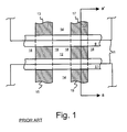
- Figure 1 illustrates a top view of a portion of a memory device formed in accordance with a conventional process.
- field oxide regions 31 and 33 are formed by growing oxide between parallel rows of nitride regions 18 to form the field oxide regions 31 and 33 as continuous lines across the source line 12 formed in the openings of a latticework of nitride regions 18.
- a layer of polysilicon is then deposited over the field oxide regions 31 and 33. After placing a photoresist mask over the polysilicon, the portions of the polysilicon left exposed are etched away. The remaining portions of polysilicon are poly word lines 9 and 11, which run parallel to source line 12.
- Etching the polysilicon to form poly word lines 9 and 11 exposes the underlying field oxide regions 31 and 33 in the region of source line 12.
- Source mask 41 is then placed over the memory device and the oxide regions 31 and 33 are then etched away where they were exposed by the etching of poly word lines 9 and 11.
- This field oxide etch which uses a high selectivity etch, as is discussed in more detail below, reduces field oxide regions 31 and 33 into separate field oxide regions 13, 15, 17 and 19. More importantly, this field oxide etch aligns field oxide regions 13 and 15, as well as 17 and 19, with the edges of poly word lines 9 and 11. Thus, when source implantation occurs it is self-aligned to the coincident edges of the field oxide and the polysilicon regions.
- the source mask 41 is not used to align the source region implantation with the edges of the poly word lines.
- the source mask 41 is placed on the memory device to protect (during implantation) the portions of the field oxide regions 31 and 33 which reside on the other side of the poly word lines 9 and 11 from the source region 12 and between which the drain regions 14 will later be formed.
- field oxide 33 is formed on the silicon substrate 29.
- Polysilicon 35 is then deposited on the field oxide 33.
- a photoresist mask 39 is then placed on top of the polysilicon 35 leaving select portions of the polysilicon exposed. Note that a direct write technique, using for example an electron beam or a laser beam, could also be used to create the mask pattern in the photoresist.
- Etching the exposed polysilicon 35 through the photoresist mask 39 of Figure 2 yields the formation, as shown in Figure 3, where the only remaining polysilicon is that which was protected by the opaque portions of photoresist mask 39.
- the remaining polysilicon portions are poly word lines 9 and 11.
- Figure 2 represents a cross- sectional view of Figure 1 along line a-a and shows the continuous field oxide layer 33 underlying poly word lines 9 and 11.
- FIG. 5 what is shown is an enlarged cutaway diagram of a FLASH EPROM cell 100 which has been processed in accordance with the prior art.
- This cell 100 comprises first and second polysilicon layers 102 and 103 and oxide region 104 therebetween, and a tunnel oxide region 106 between the first poly silicon layer 102 and the silicon area 108.
- the SAS etch 110 could effect the tunnel oxide region 106 and also could cause gouging of the implant regions 112 and 114.
- Figures 6 through 10 show the various stages of the operation of the prior art process.
- a stacked gate etch is applied to the polysilicon region 102.
- an SAS mask 202 is placed on top of the device to allow for certain portions of the oxide to be masked.
- an SAS etch 204 which essentially removes a portion of the silicon area shown in Figure 8.
- a first implant is provided, and a resist strip is applied, as is seen this implant could be brought to a position well inside the gate area of the device.
- the second implant is provided to provide the drain region shown in Figure 10.
- the resultant cell could have significant tunnel oxide erosion as well as degraded silicon doping due to silicon gouge from the SAS etch process.
- the present invention addresses these problems by using a spacer formation to protect the stacked gate edge from exposure to the SAS process. Since this spacer formation is already inherent in nearly all CMOS processes as described above with reference to Figures 1-4, existing process techniques do not have to be made significantly more complicated to provide the spacing. Through the use of this spacer formation, the SAS does not affect the doped areas nor does it affect the tunnel oxide region.
- Figure 11 is a simple flow chart showing the process in accordance with the present invention. Accordingly this process comprises providing a stacked gate edge, via step 302. The spacer formation is then provided, via step 304. Thereafter, the source aligned gate etch is provided, via step 306.
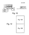
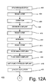
- Figure 12 shows a detailed flow chart of the process shown in Figure 11.
- Figure 12 what is shown is a flow chart of the method for protecting the tunnel oxide, stacked gate edge and source junction function profile of a device.
- the stacked gate etch takes place, via step 402.
- the resist strip takes place, via step 404.
- a thin oxide or oxidation for implant screen is provided to protect the tunnel oxide region, via step 406.
- the double diffused implant (DDI) mask and DDI implant takes place, via step 408 and another resist strip takes place, via step 410.
- the modified drain diffusion (MDD) mask and implant takes place via step 412 and another resist strip takes place, via step 413.
- a N-lightly doped drain (LDD) mask and implant and a P-LDD implant mask and implant is provided, via steps 415 and 416 and a antipunch through (AT) implant is provided, via step 418.
- LDD N-lightly doped drain
- AT antipunch through
- the spacer deposition is provided via step 420.
- the spacer is etched, via step 422.
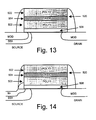
- the cross section of the core cell 500 looks like that shown in Figure 12. Accordingly, the stacked gate edge 502 is protected by the spacer formation 504. Thereafter the process for providing SAS process etch can then occur.
- an SAS mask is provided, via step 424.
- the SAS etch can be provided, via step 426.
- the spacer formation oxidation takes place, via step 428.
- the N + S/D mask and DDI mask (a critical mask) are provided, via step 430.
- the N + source/drain (S/D) implant and a source implant are provided via step 432.
- the implant step 432 is used to connect the source line from the actual source region and field region that is SAS etched.
- the cross section of the resulting cell 500 will look like that shown in Figure 14. In this cell the tunnel oxide integrity is improved and there is a uniform source region due to the spacer formation 504. Therefore, the source implant is not provided to a gouged portion of the silicon. Accordingly, a uniform source region is provided under the gate.
- tunnel oxide region integrity is much improved in addition through the use of the process of the present invention stacked gate edge is immune to gouging and as well as allowing for an improved source junction profile.
Landscapes
- Engineering & Computer Science (AREA)
- Manufacturing & Machinery (AREA)
- Non-Volatile Memory (AREA)
- Semiconductor Memories (AREA)
- Drying Of Semiconductors (AREA)
- Metal-Oxide And Bipolar Metal-Oxide Semiconductor Integrated Circuits (AREA)
Applications Claiming Priority (2)
| Application Number | Priority Date | Filing Date | Title |
|---|---|---|---|
| US08/233,174 US5470773A (en) | 1994-04-25 | 1994-04-25 | Method protecting a stacked gate edge in a semiconductor device from self aligned source (SAS) etch |
| US233174 | 1994-04-25 |
Publications (2)
| Publication Number | Publication Date |
|---|---|
| EP0680080A2 true EP0680080A2 (de) | 1995-11-02 |
| EP0680080A3 EP0680080A3 (de) | 1998-01-14 |
Family
ID=22876196
Family Applications (1)
| Application Number | Title | Priority Date | Filing Date |
|---|---|---|---|
| EP95301952A Withdrawn EP0680080A3 (de) | 1994-04-25 | 1995-03-23 | Verfahren zum Schutz der Flanken eines gestapelten Gates während des Ätzens des selbstjustierenden Sourcegebietes in einem Halbleiter-Bauelement |
Country Status (4)
| Country | Link |
|---|---|
| US (4) | US5470773A (de) |
| EP (1) | EP0680080A3 (de) |
| JP (1) | JPH07312395A (de) |
| KR (1) | KR950034806A (de) |
Cited By (1)
| Publication number | Priority date | Publication date | Assignee | Title |
|---|---|---|---|---|
| FR2850205A1 (fr) * | 2003-01-22 | 2004-07-23 | St Microelectronics Sa | Procede de fabrication d'une memoire flash et memoire flash ainsi fabriquee |
Families Citing this family (49)
| Publication number | Priority date | Publication date | Assignee | Title |
|---|---|---|---|---|
| JP3065164B2 (ja) * | 1992-03-18 | 2000-07-12 | 富士通株式会社 | 半導体装置及びその製造方法 |
| US5656509A (en) * | 1995-05-10 | 1997-08-12 | Advanced Micro Devices, Inc. | Method and test structure for determining gouging in a flash EPROM cell during SAS etch |
| JPH0982924A (ja) * | 1995-09-14 | 1997-03-28 | Toshiba Corp | 半導体記憶装置の製造方法 |
| US5854108A (en) * | 1996-06-04 | 1998-12-29 | Advanced Micro Devices, Inc. | Method and system for providing a double diffuse implant junction in a flash device |
| KR100224701B1 (ko) * | 1996-07-16 | 1999-10-15 | 윤종용 | 불휘발성 메모리장치 및 그 제조방법 |
| US5869866A (en) | 1996-12-06 | 1999-02-09 | Advanced Micro Devices, Inc. | Integrated circuit having sacrificial spacers for producing graded NMOS source/drain junctions possibly dissimilar from PMOS source/drain junctions |
| US5869879A (en) * | 1996-12-06 | 1999-02-09 | Advanced Micro Devices, Inc. | CMOS integrated circuit having a sacrificial metal spacer for producing graded NMOS source/drain junctions dissimilar from PMOS source/drain junctions |
| JP3191861B2 (ja) * | 1997-01-30 | 2001-07-23 | 日本電気株式会社 | 不揮発性半導体メモリ装置及びその消去方法 |
| US5933730A (en) * | 1997-03-07 | 1999-08-03 | Advanced Micro Devices, Inc. | Method of spacer formation and source protection after self-aligned source is formed and a device provided by such a method |
| US5930627A (en) * | 1997-05-05 | 1999-07-27 | Chartered Semiconductor Manufacturing Company, Ltd. | Process improvements in self-aligned polysilicon MOSFET technology using silicon oxynitride |
| US5895240A (en) * | 1997-06-30 | 1999-04-20 | Taiwan Semiconductor Manufacturing Company, Ltd. | Method of making stepped edge structure of an EEPROM tunneling window |
| US6004829A (en) * | 1997-09-12 | 1999-12-21 | Taiwan Semiconductor Manufacturing Company | Method of increasing end point detection capability of reactive ion etching by adding pad area |
| KR100464904B1 (ko) * | 1997-10-10 | 2005-04-19 | 삼성전자주식회사 | 자기정렬소스식각에의한터널산화막손상방지방법 |
| TW425660B (en) | 1997-12-12 | 2001-03-11 | Mosel Vitelic Inc | Method of forming uniform dielectric layer between two conductive layers in integrated circuit |
| US6025240A (en) * | 1997-12-18 | 2000-02-15 | Advanced Micro Devices, Inc. | Method and system for using a spacer to offset implant damage and reduce lateral diffusion in flash memory devices |
| US5976927A (en) * | 1998-04-10 | 1999-11-02 | Taiwan Semiconductor Manufacturing Company, Ltd. | Two mask method for reducing field oxide encroachment in memory arrays |
| US6277692B1 (en) * | 1998-05-15 | 2001-08-21 | Turbo Ic | Process for fabricating an EEPROM |
| US6124610A (en) * | 1998-06-26 | 2000-09-26 | Advanced Micro Devices, Inc. | Isotropically etching sidewall spacers to be used for both an NMOS source/drain implant and a PMOS LDD implant |
| JP2000022114A (ja) | 1998-07-02 | 2000-01-21 | Rohm Co Ltd | 半導体記憶装置およびその製造方法 |
| US6207503B1 (en) | 1998-08-14 | 2001-03-27 | Taiwan Semiconductor Manufacturing Company | Method for shrinking array dimensions of split gate flash memory device using multilayer etching to define cell and source line |
| US6103612A (en) * | 1998-09-02 | 2000-08-15 | Micron Technology, Inc. | Isolated interconnect studs and method for forming the same |
| TW406424B (en) * | 1998-09-28 | 2000-09-21 | United Microelectronics Corp | Manufacture of the flash memory |
| US6211020B1 (en) * | 1998-10-22 | 2001-04-03 | Advanced Micro Devices, Inc. | Process for fabricating a common source region in memory devices |
| KR100275746B1 (ko) | 1998-10-26 | 2000-12-15 | 윤종용 | 적층 게이트 측벽 및 활성 영역의 손상을 방지할 수 있는 비휘발성 메모리 장치의 제조 방법 |
| EP1011137A1 (de) * | 1998-12-16 | 2000-06-21 | STMicroelectronics S.r.l. | Verfahren zum Integrieren von Widerständen und ESD-Selbstschutz-Transistoren mit Speichermatrix |
| US6417041B1 (en) | 1999-03-26 | 2002-07-09 | Advanced Micro Devices, Inc. | Method for fabricating high permitivity dielectric stacks having low buffer oxide |
| US6461951B1 (en) | 1999-03-29 | 2002-10-08 | Advanced Micro Devices, Inc. | Method of forming a sidewall spacer to prevent gouging of device junctions during interlayer dielectric etching including silicide growth over gate spacers |
| US6001687A (en) * | 1999-04-01 | 1999-12-14 | Taiwan Semiconductor Manufacturing Company, Ltd. | Process for forming self-aligned source in flash cell using SiN spacer as hard mask |
| KR100295685B1 (ko) | 1999-05-10 | 2001-07-12 | 김영환 | 반도체 메모리 소자 및 그 제조방법 |
| US6579778B1 (en) | 1999-08-10 | 2003-06-17 | Advanced Micro Devices, Inc. | Source bus formation for a flash memory using silicide |
| US6236608B1 (en) | 1999-08-16 | 2001-05-22 | Alliance Semiconductor | Technique to improve the source leakage of flash EPROM cells during source erase |
| US6303959B1 (en) | 1999-08-25 | 2001-10-16 | Alliance Semiconductor Corporation | Semiconductor device having reduced source leakage during source erase |
| KR100304710B1 (ko) | 1999-08-30 | 2001-11-01 | 윤종용 | 셀 어레이 영역내에 벌크 바이어스 콘택 구조를 구비하는 비휘발성 메모리소자 |
| US6429108B1 (en) | 1999-09-02 | 2002-08-06 | Advanced Micro Devices, Inc. | Non-volatile memory device with encapsulated tungsten gate and method of making same |
| US6346467B1 (en) | 1999-09-02 | 2002-02-12 | Advanced Micro Devices, Inc. | Method of making tungsten gate MOS transistor and memory cell by encapsulating |
| US6465835B1 (en) | 1999-09-27 | 2002-10-15 | Advanced Micro Devices, Inc. | Charge gain/charge loss junction leakage prevention for flash technology by using double isolation/capping layer between lightly doped drain and gate |
| US6448608B1 (en) | 1999-09-27 | 2002-09-10 | Advanced Micro Devices, Inc. | Capping layer |
| KR20010065020A (ko) * | 1999-12-20 | 2001-07-11 | 박종섭 | 플래시 메모리장치의 제조방법 |
| KR100357185B1 (ko) | 2000-02-03 | 2002-10-19 | 주식회사 하이닉스반도체 | 비휘발성 메모리소자 및 그의 제조방법 |
| US6660585B1 (en) * | 2000-03-21 | 2003-12-09 | Aplus Flash Technology, Inc. | Stacked gate flash memory cell with reduced disturb conditions |
| US6579781B1 (en) * | 2000-07-19 | 2003-06-17 | Advanced Micro Devices, Inc. | Elimination of n+ contact implant from flash technologies by replacement with standard double-diffused and n+ implants |
| US6750157B1 (en) | 2000-10-12 | 2004-06-15 | Advanced Micro Devices, Inc. | Nonvolatile memory cell with a nitridated oxide layer |
| JP2003023114A (ja) * | 2001-07-05 | 2003-01-24 | Fujitsu Ltd | 半導体集積回路装置およびその製造方法 |
| US6680257B2 (en) * | 2001-07-30 | 2004-01-20 | Eon Silicon Devices, Inc. | Alternative related to SAS in flash EEPROM |
| US6583009B1 (en) | 2002-06-24 | 2003-06-24 | Advanced Micro Devices, Inc. | Innovative narrow gate formation for floating gate flash technology |
| US6784061B1 (en) | 2002-06-25 | 2004-08-31 | Advanced Micro Devices, Inc. | Process to improve the Vss line formation for high density flash memory and related structure associated therewith |
| JP4481557B2 (ja) | 2002-07-17 | 2010-06-16 | Okiセミコンダクタ株式会社 | 不揮発性半導体記憶装置の製造方法 |
| US7074682B2 (en) * | 2003-10-01 | 2006-07-11 | Dongbuanam Semiconductor Inc. | Method for fabricating a semiconductor device having self aligned source (SAS) crossing trench |
| US20100213140A1 (en) * | 2006-05-25 | 2010-08-26 | Haion Won | Disposable strainers for pop-up and basin drains |
Family Cites Families (12)
| Publication number | Priority date | Publication date | Assignee | Title |
|---|---|---|---|---|
| JPS6116571A (ja) * | 1984-07-03 | 1986-01-24 | Ricoh Co Ltd | 半導体装置の製造方法 |
| US5336628A (en) * | 1988-10-25 | 1994-08-09 | Commissariat A L'energie Atomique | Method for fabricating semiconductor memory device |
| US5053848A (en) * | 1988-12-16 | 1991-10-01 | Texas Instruments Incorporated | Apparatus for providing single event upset resistance for semiconductor devices |
| JPH0783066B2 (ja) * | 1989-08-11 | 1995-09-06 | 株式会社東芝 | 半導体装置の製造方法 |
| US5087584A (en) * | 1990-04-30 | 1992-02-11 | Intel Corporation | Process for fabricating a contactless floating gate memory array utilizing wordline trench vias |
| US5120671A (en) * | 1990-11-29 | 1992-06-09 | Intel Corporation | Process for self aligning a source region with a field oxide region and a polysilicon gate |
| US5149665A (en) * | 1991-07-10 | 1992-09-22 | Micron Technology, Inc. | Conductive source line for high density programmable read-only memory applications |
| US5175120A (en) * | 1991-10-11 | 1992-12-29 | Micron Technology, Inc. | Method of processing a semiconductor wafer to form an array of nonvolatile memory devices employing floating gate transistors and peripheral area having CMOS transistors |
| JP3065164B2 (ja) * | 1992-03-18 | 2000-07-12 | 富士通株式会社 | 半導体装置及びその製造方法 |
| JP3100759B2 (ja) * | 1992-06-05 | 2000-10-23 | 株式会社東芝 | 不揮発性半導体記憶装置の製造方法 |
| JP2918751B2 (ja) * | 1992-10-12 | 1999-07-12 | 株式会社東芝 | 半導体記憶装置の製造方法 |
| US5297082A (en) * | 1992-11-12 | 1994-03-22 | Micron Semiconductor, Inc. | Shallow trench source eprom cell |
-
1994
- 1994-04-25 US US08/233,174 patent/US5470773A/en not_active Expired - Lifetime
-
1995
- 1995-03-23 EP EP95301952A patent/EP0680080A3/de not_active Withdrawn
- 1995-04-18 KR KR1019950009056A patent/KR950034806A/ko not_active Ceased
- 1995-04-24 JP JP7098394A patent/JPH07312395A/ja active Pending
- 1995-05-02 US US08/433,267 patent/US5534455A/en not_active Expired - Lifetime
- 1995-06-01 US US08/460,603 patent/US5517443A/en not_active Expired - Lifetime
-
1996
- 1996-12-18 US US08/769,178 patent/US5693972A/en not_active Expired - Lifetime
Cited By (2)
| Publication number | Priority date | Publication date | Assignee | Title |
|---|---|---|---|---|
| FR2850205A1 (fr) * | 2003-01-22 | 2004-07-23 | St Microelectronics Sa | Procede de fabrication d'une memoire flash et memoire flash ainsi fabriquee |
| US7183160B2 (en) | 2003-01-22 | 2007-02-27 | Stmicroelectronics (Rousset) Sas | Manufacturing process for a flash memory and flash memory thus produced |
Also Published As
| Publication number | Publication date |
|---|---|
| US5534455A (en) | 1996-07-09 |
| US5693972A (en) | 1997-12-02 |
| JPH07312395A (ja) | 1995-11-28 |
| US5470773A (en) | 1995-11-28 |
| KR950034806A (ko) | 1995-12-28 |
| US5517443A (en) | 1996-05-14 |
| EP0680080A3 (de) | 1998-01-14 |
Similar Documents
| Publication | Publication Date | Title |
|---|---|---|
| EP0680080A2 (de) | Verfahren zum Schutz der Flanken eines gestapelten Gates während des Ätzens des selbstjustierenden Sourcegebietes in einem Halbleiter-Bauelement | |
| US5397725A (en) | Method of controlling oxide thinning in an EPROM or flash memory array | |
| US5599727A (en) | Method for producing a floating gate memory device including implanting ions through an oxidized portion of the silicon film from which the floating gate is formed | |
| KR100247862B1 (ko) | 반도체 장치 및 그 제조방법 | |
| EP0780023B1 (de) | Verfahren für selbstausgerichtete source in einem speicher hoher dichte | |
| US5612237A (en) | Method of making flash EEPROM cell | |
| KR100239459B1 (ko) | 반도체 메모리 소자 및 그 제조방법 | |
| US5464784A (en) | Method of fabricating integrated devices | |
| US6590253B2 (en) | Memory cell with self-aligned floating gate and separate select gate, and fabrication process | |
| US5798279A (en) | Method of fabricating non-volatile memories with overlapping layers | |
| US5568418A (en) | Non-volatile memory in an integrated circuit | |
| EP0934602B1 (de) | Kurzkanal-flaheeprom-speicheranordnung mit doppel-diffundierter source und verfahren zur herstellung | |
| KR100452313B1 (ko) | 비휘발성메모리소자및그제조방법 | |
| US6365449B1 (en) | Process for making a non-volatile memory cell with a polysilicon spacer defined select gate | |
| US7074682B2 (en) | Method for fabricating a semiconductor device having self aligned source (SAS) crossing trench | |
| KR100262002B1 (ko) | 플래쉬 메모리 제조방법 | |
| KR100226771B1 (ko) | 플래쉬 메모리 제조방법 | |
| KR100734075B1 (ko) | 플래쉬 메모리 셀의 구조 및 그의 제조 방법 | |
| KR0137428B1 (ko) | 플래쉬 이이피롬 제조방법 | |
| KR19990018041A (ko) | 반도체 메모리 소자 및 그의 제조방법 | |
| US6376306B1 (en) | Method for forming non volatile memory structures on a semiconductor substrate | |
| KR940009580B1 (ko) | 반도체장치의 소자분리방법 | |
| JP3783240B2 (ja) | フラッシュメモリの製造方法 | |
| KR20000042292A (ko) | 플래쉬 메모리 셀 제조방법 | |
| KR20000066702A (ko) | 플래쉬 이이피롬 셀 제조 방법 |
Legal Events
| Date | Code | Title | Description |
|---|---|---|---|
| PUAI | Public reference made under article 153(3) epc to a published international application that has entered the european phase |
Free format text: ORIGINAL CODE: 0009012 |
|
| AK | Designated contracting states |
Kind code of ref document: A2 Designated state(s): AT BE DE DK ES FR GB GR IE IT LU NL PT SE |
|
| PUAL | Search report despatched |
Free format text: ORIGINAL CODE: 0009013 |
|
| RHK1 | Main classification (correction) |
Ipc: H01L 21/8247 |
|
| AK | Designated contracting states |
Kind code of ref document: A3 Designated state(s): AT BE DE DK ES FR GB GR IE IT LU NL PT SE |
|
| 17P | Request for examination filed |
Effective date: 19980527 |
|
| 17Q | First examination report despatched |
Effective date: 20031110 |
|
| STAA | Information on the status of an ep patent application or granted ep patent |
Free format text: STATUS: THE APPLICATION IS DEEMED TO BE WITHDRAWN |
|
| 18D | Application deemed to be withdrawn |
Effective date: 20070331 |