EP0780023B1 - Verfahren für selbstausgerichtete source in einem speicher hoher dichte - Google Patents
Verfahren für selbstausgerichtete source in einem speicher hoher dichte Download PDFInfo
- Publication number
- EP0780023B1 EP0780023B1 EP96922531A EP96922531A EP0780023B1 EP 0780023 B1 EP0780023 B1 EP 0780023B1 EP 96922531 A EP96922531 A EP 96922531A EP 96922531 A EP96922531 A EP 96922531A EP 0780023 B1 EP0780023 B1 EP 0780023B1
- Authority
- EP
- European Patent Office
- Prior art keywords
- gate
- semiconductor body
- adjacent
- transistor
- spacers
- Prior art date
- Legal status (The legal status is an assumption and is not a legal conclusion. Google has not performed a legal analysis and makes no representation as to the accuracy of the status listed.)
- Expired - Lifetime
Links
Images


Classifications
-
- H—ELECTRICITY
- H10—SEMICONDUCTOR DEVICES; ELECTRIC SOLID-STATE DEVICES NOT OTHERWISE PROVIDED FOR
- H10D—INORGANIC ELECTRIC SEMICONDUCTOR DEVICES
- H10D84/00—Integrated devices formed in or on semiconductor substrates that comprise only semiconducting layers, e.g. on Si wafers or on GaAs-on-Si wafers
- H10D84/01—Manufacture or treatment
-
- H—ELECTRICITY
- H10—SEMICONDUCTOR DEVICES; ELECTRIC SOLID-STATE DEVICES NOT OTHERWISE PROVIDED FOR
- H10B—ELECTRONIC MEMORY DEVICES
- H10B41/00—Electrically erasable-and-programmable ROM [EEPROM] devices comprising floating gates
- H10B41/40—Electrically erasable-and-programmable ROM [EEPROM] devices comprising floating gates characterised by the peripheral circuit region
- H10B41/42—Simultaneous manufacture of periphery and memory cells
- H10B41/43—Simultaneous manufacture of periphery and memory cells comprising only one type of peripheral transistor
-
- H—ELECTRICITY
- H10—SEMICONDUCTOR DEVICES; ELECTRIC SOLID-STATE DEVICES NOT OTHERWISE PROVIDED FOR
- H10B—ELECTRONIC MEMORY DEVICES
- H10B69/00—Erasable-and-programmable ROM [EPROM] devices not provided for in groups H10B41/00 - H10B63/00, e.g. ultraviolet erasable-and-programmable ROM [UVEPROM] devices
-
- H—ELECTRICITY
- H10—SEMICONDUCTOR DEVICES; ELECTRIC SOLID-STATE DEVICES NOT OTHERWISE PROVIDED FOR
- H10B—ELECTRONIC MEMORY DEVICES
- H10B99/00—Subject matter not provided for in other groups of this subclass
-
- H—ELECTRICITY
- H10—SEMICONDUCTOR DEVICES; ELECTRIC SOLID-STATE DEVICES NOT OTHERWISE PROVIDED FOR
- H10D—INORGANIC ELECTRIC SEMICONDUCTOR DEVICES
- H10D84/00—Integrated devices formed in or on semiconductor substrates that comprise only semiconducting layers, e.g. on Si wafers or on GaAs-on-Si wafers
- H10D84/80—Integrated devices formed in or on semiconductor substrates that comprise only semiconducting layers, e.g. on Si wafers or on GaAs-on-Si wafers characterised by the integration of at least one component covered by groups H10D12/00 or H10D30/00, e.g. integration of IGFETs
Definitions
- This invention relates to semiconductor devices, and more particularly, to a semiconductor structure which combines memory cells with remote periphery transistors.
- Figs. 1-3 related to U.S. Patent No. 5,120,671 to Tang et al., issued June 9, 1992, show high density self-aligned-source flash memory cells fabricated by using a conventional process.
- Fig. 1 is a plan view of a portion of a memory device formed in that manner.
- Field oxide regions 10, 12 are formed as continuous lines across the source line 14 in the substrate 15.
- a gate oxide layer is formed on the substrate areas between field oxide lines, followed by deposition and patterning of a first polysilicon layer, and formation of an intergate dielectric layer.
- a second layer of polysilicon 16 is deposited and, after appropriate masking, exposed portions of the polysilicon are etched away forming control gate regions 18, 20 (word lines).
- etching steps are used to remove intergate dielectric and first polysilicon exposed between word lines.
- a photoresist mask exposing the source regions is then applied over the device.
- Exposed field oxide regions 10, 12 are etched away using an oxide etch process selective to silicon, forming a source line connecting source regions 14. This continuous source line is parallel to and self-aligned to the edges of the previously defined word lines.
- Figs. 2 and 3 are sectional views taken along the lines 2-2 and 3-3 of Fig. 1 respectively, prior to the etching of the field oxide regions 10, 12.
- Fig. 2 shows a first stack 22 made up of gate oxide 24-floating gate 26-intergate dielectric 28-control gate 30, and a second stack 32 made up of gate oxide 34-floating gate 36-intergate dielectric 38-control gate 40 with source 42 and drains 44, 46 in the substrate 48 self-aligned to the edges of the control gates 30, 40.
- the word lines 18, 20 define the control gates 30, 40 respectively and extend over the field oxide regions such as regions 10, 12 (Fig. 3).
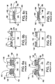
- FIG. 4 includes sectional views 4a, 4b, and 4c, Figs. 4a and 4b corresponding to the sectional views of Figs. 2 and 3, while Fig. 4c is a sectional view of a periphery transistor in the same intergated circuit.
- Figs. 5-9 follow the same convention, as do Figs. 10-14).
- a silicon substrate 130 is provided with a gate oxide 132 formed thereover.
- a first floating gate 134-intergate dielectric 136-control gate 138 stack 140 is provided on the oxide layer 132, and a second floating gate 142-intergate dielectric 144-control gate 146 stack 148 is also provided on the oxide layer 132, spaced from the stack 140.
- a source region 150 is provided in the substrate 130, self-aligned to the adjacent edges of the stacks 140, 148. Drain regions 152, 154 are also included in the substrate 130, self-aligned to the respective opposite edges of the stacks 140, 148.
- the control gates 138, 146 extend over field oxide 156 (Fig. 4b), which in turn lies over substrate 130.
- a high voltage periphery transistor 158 Remote from the structure of Figs. 4a and 4b is a high voltage periphery transistor 158 (Fig. 4c) including a gate oxide 160 on the substrate 130, and a gate 162, with lightly-doped source and drain regions 164, 166 being self-aligned to the edges of the gate 162.
- oxide 168 Over this structure is deposited a thick (for example 3000 ⁇ ) layer of oxide 168. This deposited oxide 168 is then anisotropically etched to form relatively wide spacers 170, 172, 174, 176 on the sides of each stack 140, 148, relatively wide spacers 178, 180 on the adjacent sides of the control gates 138, 146 over the field oxide 156, and relatively wide spacers 182, 184 on the sides of the gate 162 of the high voltage periphery transistor 158.
- This deposited oxide 168 is then anisotropically etched to form relatively wide spacers 170, 172, 174, 176 on the sides of each stack 140, 148, relatively wide spacers 178, 180 on the adjacent sides of the control gates 138, 146 over the field oxide 156, and relatively wide spacers 182, 184 on the sides of the gate 162 of the high voltage periphery transistor 158.
- the relatively wide spacers 182, 184 on the sides of the gate 162 of the high voltage periphery transistor 158 are properly configured so that subsequently-formed heavily doped source and drain regions will be self-aligned to the spacers 182, 184 and properly positioned in relation to the lightly doped source and drain regions 164, 166.
- Such wide spacers 182, 184 are necessary to meet high transistor junction breakdown requirements.
- provision of such relatively wide spacers 178, 180 on the inner sides of the control gates 138, 140 over the field oxide 156 causes certain problems, as will now be described.
- masking 186 is provided over appropriate areas of the structure, and further anisotropic etching is undertaken. Such etching is undertaken through the thin oxide layer 132 (Fig. 6a), and also through the field oxide 156 (Fig. 6b), it being noted that the exposed width (dimension X) of the silicon 130 due to etching through of the field oxide 156 is relatively small, because of the initial large width of the spacers 178, 180. In the meantime, etchant cannot reach the high-voltage periphery transistor 158 due to masking 186 thereover.
- a thin layer of oxide 188 is grown over the exposed portion of the silicon 130 between the stacks 140, 148, and a thin layer of oxide 190 is grown over the exposed portion of the silicon 130 provided by the opening in the field oxide 156 (Fig. 7b) simultaneously forming thin oxide layers 188, 190 and 191.
- ion implantation 194 is undertaken through the grown thin layers of oxide 188, 190, and a diffusion step is undertaken so that the source region 50 takes the shape shown in Fig. 9a, and the diffused area 196 adjacent the field oxide (Fig. 9b) provides connection between the source region 150 and other source regions. Further processing steps are then provided to form heavily doped source and drain regions 198, 200 of the periphery transistor 158, self aligned to the spacers 182, 184.
- the present invention overcomes the above-cited problems by initially forming flash memory transistor source and drain junctions and then providing a relatively thin layer of deposited oxide over floating gate-intergate dielectric-control gate stacks of flash memory transistors, over the control gate extensions on field oxide, and over the gate oxide and gate of a high voltage periphery transistor. After appropriate masking, this deposited thin oxide is etched to provide relatively narrow spacers on the adjacent sides of the stack, and on the adjacent sides of the control gate over the field oxide. The field oxide is subsequently etched through while source junctions are protected by the spacers on adjacent sides of the stacks. The deposited thin oxide over the periphery transistor is blocked by masking at this point.
- the deposited thin oxide is used as an implant blocking mask, thus saving one photoresist masking step in the process. Because the spacers are relatively narrow, the portion of silicon exposed by etching through the field oxide is relatively wide so that a relatively large width of silicon is exposed to implant, so that low series resistance between the sources of devices is provided.
- the preferred relatively wide spacers are provided on the opposite sides of the gate of the periphery transistor, so that the heavily doped source and drain regions of the periphery transistor are self-aligned to the edges of those wide spacers to render high junction breakdown for the periphery transistor.
- Fig. 10 illustrates sectional views of several areas of a partially processed flash EPROM memory device.
- Fig. 10a shows a pair of transistors as thus far formed, including a semiconductor substrate 220 of for example p-type silicon on which is provided a gate oxide 222, a first stack 224 (including a floating gate 226 on the gate oxide 222, an intergate dielectric layer 228, and a control gate 230), and a second stack 232 (including a floating gate 234 on the gate oxide 222, an intergate dielectric layer 236 and a control gate 238).
- An n-type source region 239 is provided in the substrate 220, self-aligned to the adjacent edges of the respective stacks 224, 232.
- Fig. 10b shows the structure adjacent to the structure of Fig. 10a, with extensions of the control gates 230, 238 over the field oxide 240, which in turn lies over the substrate 220
- Fig. 10c shows a high voltage remote periphery transistor 242 in an area removed from the structures of Fig. 10a and 10b, and which includes a gate oxide 244 over the substrate 220, a gate 246, and lightly doped source and drain regions 248, 250 aligned to the edges of the gate 246.
- a thin film layer 252 is deposited over the structure as shown in Fig. 10a, 10b and 10c.
- This thin film layer 252 may take the form of an oxide, nitride, polysilicon or a combination thereof, or any dielectric.
- the resulting structure is appropriately masked (254) as shown in Fig. 11, and is anisotropically etched to provide relatively narrow spacers 256, 258 on the adjacent sides of the respect stacks 224, 232, and relatively narrow spacers 260, 262 on the adjacent sides of the control gates 230, 238 over the field oxide 240.
- the etching is continued through the layer of oxide 222 and into the substrate 220, and also through the field oxide 240 down to the substrate 220. Meanwhile, the periphery transistor 242 remains covered by a photoresist mask.
- the width Y (Fig. 11b) of exposed silicon caused by etching through the field oxide 240 is relatively large.
- a thin layer of oxide is grown over the exposed silicon areas, at 264 and 266.
- Ion implantation 268 is then undertaken, self aligned to the spacers 256, 258 and spacers 260, 262, it being noted that because of the relatively thin spacers 256, 258, 260, 262, the implant covers a substantially wider area between the stacks 224, 232 and between the portions of field oxide 240 than in the prior art. It will then be seen that after diffusion of this implant (Fig. 13), the connection 269 between memory transistor sources is much wider than in the prior art, resulting in a much lower series resistance from source to source in the ultimately formed structure.
- thin film layer 252 blocks implant 268 from reaching the source and drain regions of periphery transistor 242 (Fig. 12c). Note that a resist masking step is not required to protect periphery transistors during this implant.
- Another anisotropic etch is undertaken, resulting in relatively wide spacers 280, 282 on the opposite sides of the gate 246 of the transistor 242 so that the heavily doped regions 284, 286 subsequently formed can be properly self-aligned to the sides of those spacers 280, 282 and provide proper dimensioning in regard to the lightly doped regions 248, 250.
- Flash EPROM memory Flash EPROM memory
Landscapes
- Engineering & Computer Science (AREA)
- Manufacturing & Machinery (AREA)
- Non-Volatile Memory (AREA)
- Semiconductor Memories (AREA)
Claims (18)
- Verfahren zum Herstellen einer Halbleitervorrichtung mit einer Struktur, die aufweist:mit den folgenden Schritten:(i) einen ersten Transistor mit einem Gate-Oxid (22) auf einem Halbleitersubstrat (220) und mit einer Gate-Struktur (224,232), die ein Steuer-Gate (230,238) aufweist,(ii) einen Feldoxidbereich (240), der auf dem Halbleitersubstrat (220) nahe dem ersten Transistor angeordnet ist und an dem ein erweiterter Teil des Steuer-Gates (230,238) angeordnet ist, und(iii) einen zweiten Transistor (242) mit einem Gate-Oxid (244) an dem Halbleitersubstrat (220) und einem Gate (246) an dem Gate-Oxid,Bilden einer ersten Dünnfilm-Isolierschicht (252) auf der Struktur;anisotropes Ätzen von Teilen der ersten Dünnfilm-Isolierschicht (252) über dem ersten Transistor und dem Feldoxidbereich (240) zwecks Bildung eines ersten Abstandselements (256,258) an einer Seite der Gate-Struktur (224,232), und zwecks Bildung eines zweiten Abstandselements (260,262) an einer Seite des erweiterten Teils des Steuer-Gates (230, 238), wobei das Ätzen einen nahe dem ersten Abstandselement (256, 258) gelegenen Teil des Halbleitersubstrats (220) freilegt und durch den Feldoxidbereich (240) einen nahe dem erweiterten Teil des Steuer-Gates (230,238) gelegenen Teil des Halbleitersubstrats freilegt;Implantieren von Ionen (268) in den Halbleitersubstrat;Ausbilden einer zweiten Dünnfilm-Isolierschicht (270) auf der resultierenden Struktur; undanisotropes Ätzen der resultierenden Struktur zwecks Bildung eines dritten Abstandselements (280,282) nahe einer Seite des Gates (246) des zweiten Transistors (242), wobei das dritte Abstandselement (280,282) breiter ist als das erste (256,258) und das zweite (260,262) Abstandselement.
- Verfahren nach Anspruch 1, bei dem die Implantation von Ionen mit den Seiten des ersten (256,258) und des zweiten (260,262) Abstandselements selbstausrichtend erfolgt.
- Verfahren nach Anspruch 1 oder Anspruch 2, bei dem die ersten (252) und zweiten (270) Dünnfilm-Isolierschichten jeweils ein Oxid aufweisen.
- Verfahren nach einem der Ansprüche 1 bis 3, bei dem der zweite Transistor (242) ein Hochspannungstransistor ist.
- Verfahren nach einem der vorhergehenden Ansprüche, bei dem der Source-Bereich (239) des ersten Transistors in dem Halbleitersubstrat (220) vor dem Ausbilden des ersten (256,258) und des zweiten (260,262) Abstandselements gebildet wird.
- Verfahren nach einem der vorhergehenden Ansprüche, bei dem der Drain-Bereich des ersten Transistors in dem Halbleitersubstrat (220) vor dem Ausbilden des ersten (256,258) und des zweiten (260, 262) Abstandselements gebildet wird.
- Verfahren nach einem der vorhergehenden Ansprüche, ferner mit dem Schritt des Ausbildens einer gemusterten Maske (254) im Anschluss an das Ausbilden des ersten (256,258) und des zweiten (260,262) Abstandselements, wobei die Maske (254) derart gemustert wird, dass nahe dem ersten (256,258) und dem zweiten (260,262) Abstandselement gelegene gewählte Bereiche der Struktur freigelegt werden, wenn der Feldoxidbereich (240) geätzt wird.
- Verfahren nach einem der vorhergehenden Ansprüche, bei dem die Source- und Drain-Bereiche (248,250) des zweiten Transistors (242) in dem Halbleitersubstrat (220) vor dem Ausbilden des dritten Abstandselements (280,282) gebildet werden.
- Verfahren nach einem der vorhergehenden Ansprüche, ferner mit dem Schritt des Ausbildens der Gate-Struktur (224,232) des ersten Transistors als Gate-Stapel mit Floating-Gates für dielektrische Steuerung.
- Verfahren nach einem der vorhergehenden Ansprüche, bei dem vor dem Ausbilden der zweiten Dünnfilm-Isolierschicht (270) auf der resultierenden Struktur eine Oxid-Schicht (264,266) auf dem nahe dem ersten Abstandselement (256,258) gelegenen freiliegenden Teil des Halbleitersubstrats (220) und auf dem nahe dem zweiten Abstandselement (260, 262) gelegenen freiliegenden Teil des Halbleitersubstrats (220) gezüchtet wird, und bei dem die Ionen (262) durch die gezüchtete Oxid-Schicht (264,266) und in das Halbleitersubstrat (220) implantiert werden.
- Verfahren zum Herstellen einer Halbleitervorrichtung mit einer Struktur, die aufweist:mit den folgenden Schritten:(i) ein Paar benachbarter Transistoren, jeweils mit einem Gate-Oxid (222) auf dem Halbleitersubstrat (220) und mit einer Gate-Struktur (224,232), die ein Steuer-Gate (230,238) an dem Gate-Oxid (222) aufweist, wobei das Halbleitersubstrat einen mit dem Transistoren-Paar verbundenen Source-Bereich (239) aufweist,(ii) einen Feldoxidbereich (240), der auf dem Halbleitersubstrat (220) nahe dem Transistoren-Paar angeordnet ist und an dem erweiterte Teile der Steuer-Gates (230,238) des Transistoren-Paars angeordnet sind, und(iii) einen zusätzlichen Transistor (242) mit einem Gate-Oxid (244) an dem Halbleitersubstrat (220) und einem Gate (246) an dem Gate-Oxid,Bilden einer ersten Dünnfilm-Isolierschicht (252) auf der oben beschriebenen Struktur;Ausbilden einer gemusterten Maske (254) auf der resultierenden Struktur derart, dass durch die Maske verlaufende Öffnungen definiert werden, die einen zwischen den jeweiligen Gate-Strukturen (224,232) des Transistoren-Paars gelegenen Teil der ersten Dünnfilm-Isolierschicht (252) und einen zwischen den erweiterten Teilen der Steuer-Gates (230,238) gelegenen Teil der Dünnfilm-Isolierschicht (252) freilegt;anisotropes Ätzen der freiliegenden Teile der ersten Dünnfilm-Isolierschicht (252) zwecks Bildung eines ersten Paars von Abstandselementen (256,258) an angrenzenden Seiten der jeweiligen Gate-Strukturen, und zwecks Bildung eines zweiten Paars von Abstandselementen (260, 262) an angrenzenden Seiten der jeweiligen erweiterten Teile der Steuer-Gates (230,238), wobei das Ätzen einen nahe dem Source-Bereich (239) und dem ersten Abstandselement-Paar (256,258) gelegenen Teil des Halbleitersubstrats (220) freilegt und durch das Feldoxid (240) einen nahe den erweiterten Teilen der Steuer-Gates (230,238) gelegenen Teil des Halbleitersubstrats freilegt;Entfernen der gemusterten Maske (254);Implantieren von Ionen (268) in den Halbleitersubstrat, wobei die Implantation mit den Seiten der jeweiligen Abstandselemente selbstausrichtend ist;Bilden einer zweiten Dünnfilm-Isolierschicht (270) auf der resultierenden Struktur; undanisotropes Ätzen der resultierenden Struktur zwecks Bildung eines dritten Abstandselements (280,282) nahe einer Seite des Gates (246) des zusätzlichen Transistors (242), wobei das dritte Abstandselement (280, 282) breiter ist als die ersten und zweiten Abstandselement-Paare.
- Verfahren nach Anspruch 11, bei dem die ersten (252) und zweiten (270) Dünnfilm-Isolierschichten jeweils ein Oxid aufweisen.
- Verfahren nach Anspruch 11 oder 12, bei dem der dritte Transistor ein Hochspannungstransistor ist.
- Verfahren nach einem der Ansprüche 11 bis 13, bei dem der Drain-Bereich jedes der Transistoren-Paare in dem Halbleitersubstrat (220) nahe der jeweiligen Gate-Struktur vor dem Schritt des Ausbildens des ersten (256,258) und des zweiten (260,262) Abstandselements gebildet wird.
- Verfahren nach einem der Ansprüche 11 bis 14, bei dem die Source-und Drain-Bereiche des zusätzlichen Transistors in dem Halbleitersubstrat nahe dem Gate des zusätzlichen Transistors (242) vor dem Schritt des Ausbildens der dritten Abstandselements gebildet wird.
- Verfahren nach einem der Ansprüche 11 bis 15, bei dem jede der Gate-Strukturen des Paars angrenzender Transistoren ein Gate-Stapel mit Floating-Gates für dielektrische Steuerung ist.
- Verfahren nach einem der Ansprüche 11 bis 16, bei dem vor dem Ausbilden der zweiten Dünnfilm-Isolierschicht (270) auf der resultierenden Struktur eine Oxid-Schicht (264,266) auf dem nahe dem ersten Abstandselement-Paar (256,258) gelegenen freiliegenden Teil des Siliciumsubstrats (220) und an dem nahe dem zweiten Abstandselement-Paar (260,262) gelegenen freiliegenden Teil des Siliciumsubstrats gezüchtet wird, und bei dem die Ionen durch die gezüchtete Oxid-Schicht (264,266) und in das Halbleitersubstrat implantiert werden.
- Verfahren nach einem der Ansprüche 11 bis 17, bei dem während der Implantation von Ionen in das Halbleitersubstrat die erste Dünnfilm-Isolierschicht (252) als Implantat-Blockiermaske auf dem zusätzlichen Transistor (242) verbleibt.
Applications Claiming Priority (3)
| Application Number | Priority Date | Filing Date | Title |
|---|---|---|---|
| US500648 | 1995-07-11 | ||
| US08/500,648 US5552331A (en) | 1995-07-11 | 1995-07-11 | Process for self-aligned source for high density memory |
| PCT/US1996/010698 WO1997003470A1 (en) | 1995-07-11 | 1996-06-21 | Process for self-aligned source for high density memory |
Publications (2)
| Publication Number | Publication Date |
|---|---|
| EP0780023A1 EP0780023A1 (de) | 1997-06-25 |
| EP0780023B1 true EP0780023B1 (de) | 2002-04-10 |
Family
ID=23990342
Family Applications (1)
| Application Number | Title | Priority Date | Filing Date |
|---|---|---|---|
| EP96922531A Expired - Lifetime EP0780023B1 (de) | 1995-07-11 | 1996-06-21 | Verfahren für selbstausgerichtete source in einem speicher hoher dichte |
Country Status (6)
| Country | Link |
|---|---|
| US (1) | US5552331A (de) |
| EP (1) | EP0780023B1 (de) |
| JP (1) | JP3941882B2 (de) |
| KR (1) | KR100418430B1 (de) |
| DE (1) | DE69620559T2 (de) |
| WO (1) | WO1997003470A1 (de) |
Families Citing this family (25)
| Publication number | Priority date | Publication date | Assignee | Title |
|---|---|---|---|---|
| JPH0982924A (ja) * | 1995-09-14 | 1997-03-28 | Toshiba Corp | 半導体記憶装置の製造方法 |
| JP3253552B2 (ja) * | 1996-05-31 | 2002-02-04 | 三洋電機株式会社 | 半導体装置の製造方法 |
| US5854108A (en) * | 1996-06-04 | 1998-12-29 | Advanced Micro Devices, Inc. | Method and system for providing a double diffuse implant junction in a flash device |
| KR100224701B1 (ko) * | 1996-07-16 | 1999-10-15 | 윤종용 | 불휘발성 메모리장치 및 그 제조방법 |
| JP3548834B2 (ja) * | 1996-09-04 | 2004-07-28 | 沖電気工業株式会社 | 不揮発性半導体メモリの製造方法 |
| US5933730A (en) * | 1997-03-07 | 1999-08-03 | Advanced Micro Devices, Inc. | Method of spacer formation and source protection after self-aligned source is formed and a device provided by such a method |
| GB2323706B (en) * | 1997-03-13 | 2002-02-13 | United Microelectronics Corp | Method to inhibit the formation of ion implantation induced edge defects |
| US6392267B1 (en) | 1997-04-25 | 2002-05-21 | Alliance Semiconductor Corporation | Flash EPROM array with self-aligned source contacts and programmable sector erase architecture |
| US6025240A (en) * | 1997-12-18 | 2000-02-15 | Advanced Micro Devices, Inc. | Method and system for using a spacer to offset implant damage and reduce lateral diffusion in flash memory devices |
| KR100277888B1 (ko) * | 1997-12-31 | 2001-02-01 | 김영환 | 플래쉬메모리및그의제조방법 |
| KR100269510B1 (ko) * | 1998-05-20 | 2000-10-16 | 윤종용 | 반도체 장치의 제조 방법 |
| TW461052B (en) * | 1998-06-18 | 2001-10-21 | United Microelectronics Corp | Manufacturing method of flash memory cell |
| US6140191A (en) * | 1998-09-21 | 2000-10-31 | Advanced Micro Devices, Inc. | Method of making high performance MOSFET with integrated simultaneous formation of source/drain and gate regions |
| US6713346B2 (en) | 1999-03-01 | 2004-03-30 | Micron Technology, Inc. | Methods of forming a line of flash memory cells |
| US6001687A (en) * | 1999-04-01 | 1999-12-14 | Taiwan Semiconductor Manufacturing Company, Ltd. | Process for forming self-aligned source in flash cell using SiN spacer as hard mask |
| US7012008B1 (en) | 2000-03-17 | 2006-03-14 | Advanced Micro Devices, Inc. | Dual spacer process for non-volatile memory devices |
| JP2002026156A (ja) * | 2000-07-12 | 2002-01-25 | Mitsubishi Electric Corp | 半導体装置およびその製造方法 |
| US6624022B1 (en) | 2000-08-29 | 2003-09-23 | Micron Technology, Inc. | Method of forming FLASH memory |
| US6344398B1 (en) * | 2000-10-17 | 2002-02-05 | United Microelectronics Corp. | Method for forming transistor devices with different spacer width |
| US6706601B1 (en) * | 2003-03-19 | 2004-03-16 | Taiwan Semiconductor Manufacturing Company | Method of forming tiny silicon nitride spacer for flash EPROM by using dry+wet etching technology |
| KR100561970B1 (ko) * | 2003-09-25 | 2006-03-22 | 동부아남반도체 주식회사 | 반도체 소자의 제조방법 |
| JP2006114843A (ja) * | 2004-10-18 | 2006-04-27 | Toshiba Corp | 半導体装置 |
| US7341906B2 (en) * | 2005-05-19 | 2008-03-11 | Micron Technology, Inc. | Method of manufacturing sidewall spacers on a memory device, and device comprising same |
| KR100827490B1 (ko) * | 2007-05-18 | 2008-05-06 | 주식회사 동부하이텍 | 반도체 소자의 제조 방법 |
| US10216523B2 (en) | 2015-07-17 | 2019-02-26 | General Electric Company | Systems and methods for implementing control logic |
Family Cites Families (5)
| Publication number | Priority date | Publication date | Assignee | Title |
|---|---|---|---|---|
| US5200350A (en) * | 1988-11-10 | 1993-04-06 | Texas Instruments Incorporated | Floating-gate memory array with silicided buried bitlines |
| FR2642900B1 (fr) * | 1989-01-17 | 1991-05-10 | Sgs Thomson Microelectronics | Procede de fabrication de circuits integres a transistors de memoire eprom et a transistors logiques |
| US5087584A (en) * | 1990-04-30 | 1992-02-11 | Intel Corporation | Process for fabricating a contactless floating gate memory array utilizing wordline trench vias |
| US5147813A (en) * | 1990-08-15 | 1992-09-15 | Intel Corporation | Erase performance improvement via dual floating gate processing |
| US5439835A (en) * | 1993-11-12 | 1995-08-08 | Micron Semiconductor, Inc. | Process for DRAM incorporating a high-energy, oblique P-type implant for both field isolation and punchthrough |
-
1995
- 1995-07-11 US US08/500,648 patent/US5552331A/en not_active Expired - Lifetime
-
1996
- 1996-06-21 WO PCT/US1996/010698 patent/WO1997003470A1/en not_active Ceased
- 1996-06-21 DE DE69620559T patent/DE69620559T2/de not_active Expired - Lifetime
- 1996-06-21 JP JP50582297A patent/JP3941882B2/ja not_active Expired - Fee Related
- 1996-06-21 EP EP96922531A patent/EP0780023B1/de not_active Expired - Lifetime
- 1996-06-21 KR KR1019970701600A patent/KR100418430B1/ko not_active Expired - Fee Related
Also Published As
| Publication number | Publication date |
|---|---|
| KR100418430B1 (ko) | 2004-05-20 |
| US5552331A (en) | 1996-09-03 |
| JPH10505961A (ja) | 1998-06-09 |
| DE69620559T2 (de) | 2002-11-21 |
| KR970705837A (ko) | 1997-10-09 |
| JP3941882B2 (ja) | 2007-07-04 |
| DE69620559D1 (de) | 2002-05-16 |
| EP0780023A1 (de) | 1997-06-25 |
| WO1997003470A1 (en) | 1997-01-30 |
Similar Documents
| Publication | Publication Date | Title |
|---|---|---|
| EP0780023B1 (de) | Verfahren für selbstausgerichtete source in einem speicher hoher dichte | |
| US5019527A (en) | Method of manufacturing non-volatile semiconductor memories, in which selective removal of field oxidation film for forming source region and self-adjusted treatment for forming contact portion are simultaneously performed | |
| US5397725A (en) | Method of controlling oxide thinning in an EPROM or flash memory array | |
| EP0680080A2 (de) | Verfahren zum Schutz der Flanken eines gestapelten Gates während des Ätzens des selbstjustierenden Sourcegebietes in einem Halbleiter-Bauelement | |
| US5017515A (en) | Process for minimizing lateral distance between elements in an integrated circuit by using sidewall spacers | |
| KR19990048973A (ko) | 반도체 장치 및 그 제조방법 | |
| KR980012623A (ko) | 전계 효과 트랜지스터 및 그 제조방법 | |
| US5070029A (en) | Semiconductor process using selective deposition | |
| KR100199381B1 (ko) | 플래쉬 이이피롬 셀 제조 방법 | |
| GB2078443A (en) | Fabricating memory cells in semiconductor integrated circuits | |
| KR100470990B1 (ko) | 메모리셀영역과주변로직영역트랜지스터의게이트적층형태가상이한반도체장치의제조방법 | |
| JPH04349670A (ja) | 不揮発性半導体記憶装置の製造方法 | |
| KR100313543B1 (ko) | 플랫 롬 제조방법 | |
| KR0172271B1 (ko) | 플래쉬 이이피롬 셀의 제조방법 | |
| KR0155827B1 (ko) | 불휘발성 반도체 장치의 소자분리방법 | |
| KR0123745B1 (ko) | 반도체 장치의 콘택 형성방법 | |
| KR100537273B1 (ko) | 반도체 소자 제조방법 | |
| KR930008080B1 (ko) | 불휘발성 메모리장치의 제조방법 | |
| KR970011758B1 (ko) | 반도체 집적회로의 전도막 형성방법 | |
| JP3783240B2 (ja) | フラッシュメモリの製造方法 | |
| KR100314731B1 (ko) | 멀티비트플래쉬메모리장치의제조방법 | |
| KR960012262B1 (ko) | 모스(mos) 트랜지스터 제조방법 | |
| KR0137428B1 (ko) | 플래쉬 이이피롬 제조방법 | |
| KR100280490B1 (ko) | 반도체 소자의 분리구조 형성방법 | |
| KR19980035608A (ko) | 반도체소자 제조방법 |
Legal Events
| Date | Code | Title | Description |
|---|---|---|---|
| PUAI | Public reference made under article 153(3) epc to a published international application that has entered the european phase |
Free format text: ORIGINAL CODE: 0009012 |
|
| 17P | Request for examination filed |
Effective date: 19970313 |
|
| AK | Designated contracting states |
Kind code of ref document: A1 Designated state(s): DE FR GB IT |
|
| 17Q | First examination report despatched |
Effective date: 19991214 |
|
| GRAG | Despatch of communication of intention to grant |
Free format text: ORIGINAL CODE: EPIDOS AGRA |
|
| GRAG | Despatch of communication of intention to grant |
Free format text: ORIGINAL CODE: EPIDOS AGRA |
|
| GRAH | Despatch of communication of intention to grant a patent |
Free format text: ORIGINAL CODE: EPIDOS IGRA |
|
| REG | Reference to a national code |
Ref country code: GB Ref legal event code: IF02 |
|
| GRAH | Despatch of communication of intention to grant a patent |
Free format text: ORIGINAL CODE: EPIDOS IGRA |
|
| GRAA | (expected) grant |
Free format text: ORIGINAL CODE: 0009210 |
|
| AK | Designated contracting states |
Kind code of ref document: B1 Designated state(s): DE FR GB IT |
|
| PG25 | Lapsed in a contracting state [announced via postgrant information from national office to epo] |
Ref country code: IT Free format text: LAPSE BECAUSE OF FAILURE TO SUBMIT A TRANSLATION OF THE DESCRIPTION OR TO PAY THE FEE WITHIN THE PRESCRIBED TIME-LIMIT;WARNING: LAPSES OF ITALIAN PATENTS WITH EFFECTIVE DATE BEFORE 2007 MAY HAVE OCCURRED AT ANY TIME BEFORE 2007. THE CORRECT EFFECTIVE DATE MAY BE DIFFERENT FROM THE ONE RECORDED. Effective date: 20020410 |
|
| REF | Corresponds to: |
Ref document number: 69620559 Country of ref document: DE Date of ref document: 20020516 |
|
| ET | Fr: translation filed | ||
| PLBE | No opposition filed within time limit |
Free format text: ORIGINAL CODE: 0009261 |
|
| STAA | Information on the status of an ep patent application or granted ep patent |
Free format text: STATUS: NO OPPOSITION FILED WITHIN TIME LIMIT |
|
| 26N | No opposition filed |
Effective date: 20030113 |
|
| REG | Reference to a national code |
Ref country code: GB Ref legal event code: 732E |
|
| PGFP | Annual fee paid to national office [announced via postgrant information from national office to epo] |
Ref country code: GB Payment date: 20140627 Year of fee payment: 19 |
|
| PGFP | Annual fee paid to national office [announced via postgrant information from national office to epo] |
Ref country code: DE Payment date: 20140627 Year of fee payment: 19 |
|
| PGFP | Annual fee paid to national office [announced via postgrant information from national office to epo] |
Ref country code: FR Payment date: 20140617 Year of fee payment: 19 |
|
| REG | Reference to a national code |
Ref country code: GB Ref legal event code: 732E Free format text: REGISTERED BETWEEN 20150618 AND 20150624 |
|
| REG | Reference to a national code |
Ref country code: DE Ref legal event code: R082 Ref document number: 69620559 Country of ref document: DE Representative=s name: MURGITROYD & COMPANY, DE Ref country code: DE Ref legal event code: R081 Ref document number: 69620559 Country of ref document: DE Owner name: CYPRESS SEMICONDUCTOR CORP. (N.D.GES.D.STAATES, US Free format text: FORMER OWNER: SPANSION LLC (N.D.GES.D. STAATES DELAWARE), SUNNYVALE, CALIF., US |
|
| REG | Reference to a national code |
Ref country code: FR Ref legal event code: TP Owner name: CYPRESS SEMICONDUCTOR CORPORATION, US Effective date: 20151124 |
|
| REG | Reference to a national code |
Ref country code: DE Ref legal event code: R119 Ref document number: 69620559 Country of ref document: DE |
|
| GBPC | Gb: european patent ceased through non-payment of renewal fee |
Effective date: 20150621 |
|
| REG | Reference to a national code |
Ref country code: FR Ref legal event code: ST Effective date: 20160229 |
|
| PG25 | Lapsed in a contracting state [announced via postgrant information from national office to epo] |
Ref country code: GB Free format text: LAPSE BECAUSE OF NON-PAYMENT OF DUE FEES Effective date: 20150621 Ref country code: DE Free format text: LAPSE BECAUSE OF NON-PAYMENT OF DUE FEES Effective date: 20160101 |
|
| PG25 | Lapsed in a contracting state [announced via postgrant information from national office to epo] |
Ref country code: FR Free format text: LAPSE BECAUSE OF NON-PAYMENT OF DUE FEES Effective date: 20150630 |