EP0680143A2 - Circuit de résistance terminale CMOS - Google Patents
Circuit de résistance terminale CMOS Download PDFInfo
- Publication number
- EP0680143A2 EP0680143A2 EP95104588A EP95104588A EP0680143A2 EP 0680143 A2 EP0680143 A2 EP 0680143A2 EP 95104588 A EP95104588 A EP 95104588A EP 95104588 A EP95104588 A EP 95104588A EP 0680143 A2 EP0680143 A2 EP 0680143A2
- Authority
- EP
- European Patent Office
- Prior art keywords
- resistor
- current mirror
- circuit
- differential amplifier
- cmos
- Prior art date
- Legal status (The legal status is an assumption and is not a legal conclusion. Google has not performed a legal analysis and makes no representation as to the accuracy of the status listed.)
- Withdrawn
Links
- 230000005540 biological transmission Effects 0.000 claims abstract description 34
- 238000005516 engineering process Methods 0.000 description 9
- 230000000694 effects Effects 0.000 description 3
- 238000013459 approach Methods 0.000 description 2
- 239000003990 capacitor Substances 0.000 description 2
- 238000011161 development Methods 0.000 description 2
- 238000007667 floating Methods 0.000 description 2
- 230000001105 regulatory effect Effects 0.000 description 2
- JBRZTFJDHDCESZ-UHFFFAOYSA-N AsGa Chemical compound [As]#[Ga] JBRZTFJDHDCESZ-UHFFFAOYSA-N 0.000 description 1
- 229910001218 Gallium arsenide Inorganic materials 0.000 description 1
- 230000006399 behavior Effects 0.000 description 1
- 230000033228 biological regulation Effects 0.000 description 1
- 230000008878 coupling Effects 0.000 description 1
- 238000010168 coupling process Methods 0.000 description 1
- 238000005859 coupling reaction Methods 0.000 description 1
- 230000007423 decrease Effects 0.000 description 1
- 238000013461 design Methods 0.000 description 1
- 230000006870 function Effects 0.000 description 1
- 230000010354 integration Effects 0.000 description 1
- 238000004519 manufacturing process Methods 0.000 description 1
- 239000011159 matrix material Substances 0.000 description 1
- 230000015654 memory Effects 0.000 description 1
- 229910052751 metal Inorganic materials 0.000 description 1
- 239000002184 metal Substances 0.000 description 1
- 238000012856 packing Methods 0.000 description 1
- 230000003071 parasitic effect Effects 0.000 description 1
- 229910021420 polycrystalline silicon Inorganic materials 0.000 description 1
- 229920005591 polysilicon Polymers 0.000 description 1
- 230000001681 protective effect Effects 0.000 description 1
- 239000004065 semiconductor Substances 0.000 description 1
- 230000008054 signal transmission Effects 0.000 description 1
- 238000004088 simulation Methods 0.000 description 1
Images


Classifications
-
- H—ELECTRICITY
- H03—ELECTRONIC CIRCUITRY
- H03H—IMPEDANCE NETWORKS, e.g. RESONANT CIRCUITS; RESONATORS
- H03H11/00—Networks using active elements
- H03H11/02—Multiple-port networks
- H03H11/28—Impedance matching networks
- H03H11/30—Automatic matching of source impedance to load impedance
Definitions
- lines with a defined characteristic impedance must be used to transmit very high data rates between integrated components and terminated at the end of the line with a resistance that corresponds to the characteristic impedance of the line. Otherwise, reflections and thus interference occur, which are superimposed on the useful signal and can lead to bit errors at the receiver.
- CMOS devices Data rates in the range from approx. 100 Mbit / s to 1 Gbit / s were previously reserved for bipolar or gallium arsenide components in integrated circuits; Due to advances in semiconductor technology, CMOS devices have now also reached this speed range. When transmitting such high data rates, termination resistors are therefore also required at the inputs of CMOS devices.
- the termination resistors of CMOS devices have been arranged outside the device on the circuit board close to the corresponding input pins.
- Modules of switching systems such as switching matrix modules, or of computers, such as memories with address and data lines, can have a large number of inputs, so that the associated terminating resistors require a significant amount of space, which reduces the packing density on the module.
- the termination is not made directly at the input stage of the receiver module; rather, there is still the housing of the module and the protective structures against electrostatic charge, which are necessary with CMOS modules, between the terminating resistor and the input stage.
- the housing essentially consists of line inductances and capacitors such as pin and bond inductors and parasitic load capacitors; there are also coupling inductances and capacitances between the pins.
- the path from the external terminating resistor to the input stage can be regarded as an incomplete line, which leads to reflections which make it difficult to transmit high frequencies. Terminating resistors for IC components are known, for example, from Safferthal: “Terminating signal lines", Electronics 22/1990, pages 236 ... 254.
- the object of the present invention is now to specify the implementation of an exact terminating resistor in CMOS technology.
- the invention relates to a CMOS termination circuit; According to the invention, this terminating circuit is characterized in that the terminating resistor is formed by a CMOS transmission gate which is connected with its control electrodes to the control electrodes of an integrated reference transmission gate.
- the invention has the advantage of enabling precise internal terminating resistors in CMOS technology and thus being able to dispense with external terminating resistors, reducing the space requirement and achieving higher integration on the module; at the same time, the high-frequency behavior is improved, so that higher bit rates are possible.
- the current mirror transistor in series with the external reference resistor can also be connected in parallel with the input circuit of a comparator provided with a reference voltage source, the output of which leads directly or via an inverter to the control inputs of two opposite CMOS transistors, one of which has its own Main electrodes between ground and the output line of one differential amplifier and the other with its main electrodes between the supply potential source and the output line of the other differential amplifier lies.
- the terminating resistor is implemented according to the invention with a so-called transmission gate.
- a transmission gate basically consists of a p-channel transistor and an n-channel transistor connected in parallel.
- the use of a transmission gate as a resistor is known per se in CMOS technology.
- the transistors are operated in the resistance range of their characteristic curves, ie the fact is used that a MOS transistor behaves like a linear ohmic resistor between drain and source connection for sufficiently low drain-source voltages.
- the resistance value depends on the gate-source voltage and can therefore be set.
- the transmission gate TG forms, together with a current mirror transistor SA, a current mirror circuit TD, SA, SB fed by a reference current source J, a series circuit TG-SA, which is parallel to another one formed by the external reference resistor R and a further current mirror transistor SB Series circuit R-SB is connected to a termination potential source U which corresponds to the desired termination potential with its voltage.
- the one control electrode of the transmission gate TG is connected to the output of a first operational amplifier DV1 connected as a differential amplifier; its other control electrode is connected to the output of a second operational amplifier connected downstream of the differential amplifier DV1 via its inverting input and connected as an inverting amplifier.
- Its series resistor R1 and feedback resistor R2 expediently have the same resistance values, so that the gain is 1.
- the two inputs of the differential amplifier DV1 are connected to the two inner connection points A, B of the two series circuits TG-SA, R-SB, ie to the connection point A between the transmission gate TG and the current mirror -Transistor SA or with the connection point B between reference resistor R and current mirror transistor SB.
- the transistors TD, SA, SB of the current mirror circuit advantageously each have the same channel lengths or widths; then the current flowing through the current mirror transistors SA, SB is in each case just as large as the current flowing through the diode transistor TD, ie the reference current J is mirrored by the diode transistor TD onto the current mirror transistors SA and SB.
- the generation of a reference current is widely known from the literature (for example Paul R. Gray, Robert G. Meyer, "Analysis and Design of Analog Integrated Circuits", John Wiley & Sons, New York, 1984) and need not be explained further here .
- the differential amplifier DV1 compares the voltages at points A and B and generates an output voltage U GN which controls the resistance of the n-channel transistor in the transmission gate via the corresponding control input of the transmission gate TG.
- the inverting amplifier DV2 controls the resistance of the p-channel transistor in the transmission gate with its output voltage U GP .
- the resistors R1 and R2 of the inverting amplifier DV2 can be implemented in CMOS technology as well resistors, since the gain setting depends only on the ratio of the resistance values, but not on the absolute values.
- the p-channel transistor and the n-channel transistor of the transmission gate TG are of the same magnitude and have the opposite sign; both transistors thus become more or less conductive in the same direction. If the potential at node B in the circuit arrangement according to FIG. 1 is more positive than at node A, this means that the resistance value of the transmission gate TG is greater than that of the reference resistor R, since the same currents flow through both.
- control voltage U GN increases and the control voltage U GP falls, so that the transmission gate TG is further opened and thus its resistance is reduced until the resistance values of the transmission gate TG and the reference resistor R are the same and the circuit points A and B are at the same potential.
- the resistance value of the internal, ie integrated, transmission gate TG is automatically regulated to the value of the external resistance R.
- the control voltages U GN and U GP can then be used to control the actual terminating resistor be used.
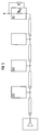
- 1 shows a differential input with two transmission gates TG1 and TG2 as the termination of two input terminals e1, e2.
- the transmission gates TG1 and TG2, like the transmission gate TG, are dimensioned and placed close to them, so that they are identical to the extent that the transmission gate TG is used and the same resistance value is set on them by the control voltages U GN and U GP .
- the resistance value of the external resistor R can be increased while the size of the current flowing through it is reduced accordingly. If the resistor R has, for example, 10 times the value of the desired terminating resistor, then the value of the current flowing through the current mirror transistor SB must be one tenth of the value of the reference current J in order to obtain the same potential again at the connection points A and B. This can easily be achieved on the current mirror by dimensioning the width of the current mirror transistor SB to a tenth of the width of the current mirror transistor SA.
- Such a floating terminating resistor (R AE in Figure 3) can in turn by means of a transmission gate (TG AE in the in the rest of Fig.2) explained below, which is controlled in the manner explained with reference to FIG. 1 by the output voltages U GN and U GP of a differential amplifier DV1 and an inverting amplifier DV2 connected downstream of it, the differential amplifier DV1 with its an input terminal at the connection point of the series circuit of a reference transmission gate TG and a current mirror transistor SA and with its other input terminal at the connection point of the series circuit of a reference resistor R and a current mirror transistor SB.
- TG AE in Figure 3 Such a floating terminating resistor (R AE in Figure 3) can in turn by means of a transmission gate (TG AE in the in the rest of Fig.2) explained below, which is controlled in the manner explained with reference to FIG. 1 by the output voltages U GN and U GP of a differential amplifier DV1 and an inverting amplifier DV2 connected downstream of it, the differential
- An optimal setting for the reference resistance R is achieved if the voltage U across the series circuits TG-SA, R-SB is placed approximately in the middle between the high and low levels of the input signal. If the DC component of the input signal is unknown or can change, the voltage U is expediently chosen to be equal to half the supply voltage. The further the common-mode component of the input signal is away from the value U, the more the resistance value of the transmission gate at the input to be terminated can differ from that of the reference resistor R. This creates a compensation effect: If, for example, the common-mode component approaches ground potential, the resistance of the p-channel transistor of the transmission gate increases.
- the gate-source voltage of the n-channel transistor rises, and consequently the resistance of the n-channel transistor decreases. In this way, the increase in the resistance of the p-channel transistor is largely compensated for. If the common mode component approaches the supply voltage U DD , the same compensation effect occurs on the p-channel transistor.
- a center level of 1.2 V (based on the ground potential of the transmitter) is defined between the signal levels high and low; in this respect a termination voltage U of 1.2 V would be desirable. Since the working range for the circuit according to FIG. 1 may then be somewhat tight, the terminating voltage U can be chosen to be half the supply voltage, as has already been described above. If necessary, however, it is more advantageous to then implement the current mirror with p-channel transistors instead of with n-channel transistors and to connect them to the supply potential source U DD ; the reference current source must then be turned over. The voltages are then related to U DD and there is therefore a larger voltage range available for the control circuit.
- FIG. 2 Such a CMOS terminating resistor circuit for a floating terminating resistor TG AE is outlined in FIG. 2.
- the function of this terminating resistor circuit is basically the same as that of the terminating resistor circuit according to FIG. 1, so that no further explanations are required here.
- the specification of the SCI-LVDS interface sketched in Fig. 3 also requires a certain internal resistance for the output of the transmitter module, so that no reflections occur at the output even with return waves that may occur due to asymmetries or interference. If the output stage of the transmitter works as a current source, which sends an impressed current to the line, the output is high-resistance, and a terminating resistor R AS must also be integrated between the output lines.
- the regulated transmission gate described with reference to FIG. 2 can also advantageously be used for this.
- signals or clocks are often to be transmitted in their switching fields from a transmission module not only to a single CMOS reception module, but to a whole series of CMOS reception modules which are connected to the same line carrying the signal or the clock , the line being terminated at the last module with a terminating resistor.
- a transmission module not only to a single CMOS reception module, but to a whole series of CMOS reception modules which are connected to the same line carrying the signal or the clock , the line being terminated at the last module with a terminating resistor.
- CMOS modules are designated here with IC1, IC2, ..., ICl.
- the line termination at the last module IC1 can be effected by means of a CMOS terminating resistor circuit according to the invention, while the inputs of the other modules must be high-resistance.
- a further embodiment of the invention can now be used in series in the individual terminating resistor circuits, as outlined in FIG to the external reference resistor R current mirror transistor SB the input circuit of a comparator DV3 provided with a reference voltage source U ref , the output of which leads directly or via an inverter I to the control inputs of two MOS transistors of opposite channel type, one of which with its main electrodes between ground and the output line of one differential amplifier DV1 and the other of which lies with its main electrodes between the supply potential source U DD and the output line of the other differential amplifier DV2.
- the external reference resistor R current mirror transistor SB the input circuit of a comparator DV3 provided with a reference voltage source U ref , the output of which leads directly or via an inverter I to the control inputs of two MOS transistors of opposite channel type, one of which with its main electrodes between ground and the output line of one differential amplifier DV1 and the other of which lies with its main electrodes between the supply potential source U DD and the output line of the other differential amplifier
- the external resistor R, the current mirror transistor SB and the first differential amplifier DV1 of the remaining terminating resistor circuit are also shown on the left, as is shown in further circuitry details in the example in FIG.
- an additional differential amplifier is provided as the comparator DV3, its non-inverting input with the reference voltage source U ref is connected.
- the reference voltage must be less than the voltage occurring in control mode at node B. Then the output of the comparator is in the low state, that is to say in the vicinity of the ground potential, and the directly following n-channel transistor TN and the p-channel transistor TP following via the inverter I are non-conductive and thus take on the control voltage lines U GN , U GP (in FIG. 4 and FIG. 1) have no influence on the regulation of the terminating resistance value.
- the reference voltage can be derived, for example, from the supply voltage by voltage division with the aid of trough resistors, without this requiring further explanation.
- the current mirror transistor SB pulls the node B to ground potential, the output of the comparator DV3 goes high, and that both transistors TN and TP switch through.
- the two transistors TN and TP should be stronger than the output transistors of the two differential amplifiers DV1 and DV2 due to the dimensioning.
- the output line U GN reaches the ground potential and the output line U GP reaches the supply potential U DD with the result that the transmission gates (TG in the control circuit and TG1, TG2 (or TG AE ) at the inputs) assume high resistance values ; the internal terminating resistors are switched off.
- the external reference resistor (R in FIG. 4) is thus omitted for all CMOS chips IC1, ..., with the exception of the last one, and only this last external CMOS chip IC1 can be seen Reference resistor in front with the result that the line leading to the CMOS chips IC1, ..., ICl is properly terminated at its end by the CMOS chip ICl.
Landscapes
- Logic Circuits (AREA)
- Semiconductor Integrated Circuits (AREA)
- Networks Using Active Elements (AREA)
Applications Claiming Priority (2)
| Application Number | Priority Date | Filing Date | Title |
|---|---|---|---|
| DE4412055A DE4412055C1 (de) | 1994-04-07 | 1994-04-07 | CMOS-Abschlußwiderstandsschaltung |
| DE4412055 | 1994-04-07 |
Publications (2)
| Publication Number | Publication Date |
|---|---|
| EP0680143A2 true EP0680143A2 (fr) | 1995-11-02 |
| EP0680143A3 EP0680143A3 (fr) | 1996-07-03 |
Family
ID=6514866
Family Applications (1)
| Application Number | Title | Priority Date | Filing Date |
|---|---|---|---|
| EP95104588A Withdrawn EP0680143A3 (fr) | 1994-04-07 | 1995-03-28 | Circuit de résistance terminale CMOS. |
Country Status (4)
| Country | Link |
|---|---|
| US (1) | US5559448A (fr) |
| EP (1) | EP0680143A3 (fr) |
| JP (1) | JPH07297678A (fr) |
| DE (1) | DE4412055C1 (fr) |
Cited By (1)
| Publication number | Priority date | Publication date | Assignee | Title |
|---|---|---|---|---|
| EP0756783B1 (fr) * | 1994-04-22 | 2004-04-14 | Unitrode Corporation | Emulateur d'impedance |
Families Citing this family (34)
| Publication number | Priority date | Publication date | Assignee | Title |
|---|---|---|---|---|
| JPH07235952A (ja) * | 1993-12-28 | 1995-09-05 | Oki Electric Ind Co Ltd | 信号伝送回路およびその回路を用いた信号伝送装置 |
| US6037798A (en) * | 1996-05-08 | 2000-03-14 | Telefonaktiebolaget Lm Ericsson | Line receiver circuit having termination impedances with transmission gates connected in parallel |
| US6570561B1 (en) * | 1996-06-14 | 2003-05-27 | Texas Instruments Incorporated | Portable computer with low voltage differential signaling adapter |
| US6044110A (en) * | 1996-08-15 | 2000-03-28 | Lsi Logic Corporation | Method and apparatus for transmission line equalization |
| US5926031A (en) * | 1996-10-29 | 1999-07-20 | Linfinitymicroelectronics, Inc. | High speed digital bus termination |
| US6008665A (en) * | 1997-05-07 | 1999-12-28 | California Micro Devices Corporation | Termination circuits and methods therefor |
| US6157206A (en) * | 1998-12-31 | 2000-12-05 | Intel Corporation | On-chip termination |
| US6294937B1 (en) | 1999-05-25 | 2001-09-25 | Lsi Logic Corporation | Method and apparatus for self correcting parallel I/O circuitry |
| US6557066B1 (en) | 1999-05-25 | 2003-04-29 | Lsi Logic Corporation | Method and apparatus for data dependent, dual level output driver |
| US6130548A (en) * | 1999-07-09 | 2000-10-10 | Motorola Inc. | Signal converting receiver having constant hysteresis, and method therefor |
| US6181170B1 (en) | 1999-07-09 | 2001-01-30 | Motorola Inc. | Driver having substantially constant and linear output resistance, and method therefor |
| US6356113B1 (en) | 1999-12-28 | 2002-03-12 | International Business Machines Corp. | Recording channel with voltage-type write driver for use with transmission-line interconnect |
| US6424169B1 (en) | 2000-01-24 | 2002-07-23 | Broadcom Corporation | Active termination network |
| US6816987B1 (en) | 2000-03-25 | 2004-11-09 | Broadcom Corporation | Apparatus and method for built-in self-test of a data communications system |
| US6356103B1 (en) * | 2000-05-30 | 2002-03-12 | International Business Machines Corporation | CMOS small signal terminator and network |
| US6605958B2 (en) * | 2000-10-11 | 2003-08-12 | Vitesse Semiconductor Corporation | Precision on-chip transmission line termination |
| DE10115740A1 (de) | 2001-03-26 | 2002-10-02 | Ulrich Speck | Zubereitung für die Restenoseprophylaxe |
| US6744275B2 (en) * | 2002-02-01 | 2004-06-01 | Intel Corporation | Termination pair for a differential driver-differential receiver input output circuit |
| JP2003298395A (ja) * | 2002-04-04 | 2003-10-17 | Mitsubishi Electric Corp | 差動終端抵抗調整回路 |
| DE10244847A1 (de) * | 2002-09-20 | 2004-04-01 | Ulrich Prof. Dr. Speck | Medizinische Vorrichtung zur Arzneimittelabgabe |
| DE10251473B3 (de) * | 2002-11-05 | 2004-06-17 | Siemens Ag | Schutzschaltung zum Schutz gegen Überspannung für einen CAN-Bus-Transceiver |
| KR100729916B1 (ko) * | 2004-04-08 | 2007-06-18 | 주식회사 하이닉스반도체 | 온 다이 터미네이션 회로 |
| US7417452B1 (en) | 2006-08-05 | 2008-08-26 | Altera Corporation | Techniques for providing adjustable on-chip termination impedance |
| US7423450B2 (en) * | 2006-08-22 | 2008-09-09 | Altera Corporation | Techniques for providing calibrated on-chip termination impedance |
| US7940077B2 (en) * | 2006-09-05 | 2011-05-10 | Lecroy Corporation | Adjustable resistance |
| JP4711940B2 (ja) * | 2006-12-08 | 2011-06-29 | 株式会社東芝 | 半導体集積回路およびこの半導体集積回路の終端抵抗の測定方法 |
| US7372295B1 (en) | 2006-12-22 | 2008-05-13 | Altera Corporation | Techniques for calibrating on-chip termination impedances |
| US7443193B1 (en) | 2006-12-30 | 2008-10-28 | Altera Corporation | Techniques for providing calibrated parallel on-chip termination impedance |
| US8290445B2 (en) * | 2007-08-10 | 2012-10-16 | Panasonic Corporation | Electronic device, and information apparatus, communications apparatus, AV apparatus, and mobile apparatus using the same |
| WO2009122462A1 (fr) | 2008-03-31 | 2009-10-08 | 富士通株式会社 | Circuit à borne, dispositif à semi-conducteur et dispositif électronique |
| JP2010268350A (ja) * | 2009-05-18 | 2010-11-25 | Renesas Electronics Corp | 終端抵抗調整回路 |
| US9647663B1 (en) * | 2016-06-27 | 2017-05-09 | Altera Corporation | Differential input buffer circuits and methods |
| CN111431522B (zh) * | 2020-04-22 | 2023-05-12 | 上海微阱电子科技有限公司 | 一种能够兼容输出的mipi驱动电路 |
| KR20250054628A (ko) * | 2023-10-16 | 2025-04-23 | 에스케이하이닉스 주식회사 | 전압제어발진기를 위한 초기 제어전압 생성회로 및 이를 포함하는 위상고정루프 회로 |
Family Cites Families (9)
| Publication number | Priority date | Publication date | Assignee | Title |
|---|---|---|---|---|
| US4859877A (en) * | 1988-01-04 | 1989-08-22 | Gte Laboratories Incorporated | Bidirectional digital signal transmission system |
| US5071660A (en) * | 1988-06-10 | 1991-12-10 | Phillips Petroleum Company | Process utilizing alcohol oxidase |
| FR2674076A1 (fr) * | 1991-03-14 | 1992-09-18 | Bull Sa | Circuit integre a impedances asservies et application aux emetteurs-recepteurs notamment pour la communication entre unites d'un systeme informatique. |
| US5283479A (en) * | 1991-04-30 | 1994-02-01 | Microunity Systems Engineering, Inc. | BiCMOS logic gate having plural linearly operated load FETs |
| US5124580A (en) * | 1991-04-30 | 1992-06-23 | Microunity Systems Engineering, Inc. | BiCMOS logic gate having linearly operated load FETs |
| US5254883A (en) * | 1992-04-22 | 1993-10-19 | Rambus, Inc. | Electrical current source circuitry for a bus |
| US5422608A (en) * | 1992-09-23 | 1995-06-06 | Texas Instruments Incorporated | Adaptive transmission line termination |
| US5329184A (en) * | 1992-11-05 | 1994-07-12 | National Semiconductor Corporation | Method and apparatus for feedback control of I/O characteristics of digital interface circuits |
| US5396028A (en) * | 1993-05-05 | 1995-03-07 | Texas Instruments Incorporated | Method and apparatus for transmission line termination |
-
1994
- 1994-04-07 DE DE4412055A patent/DE4412055C1/de not_active Expired - Fee Related
-
1995
- 1995-03-28 EP EP95104588A patent/EP0680143A3/fr not_active Withdrawn
- 1995-04-07 US US08/418,367 patent/US5559448A/en not_active Expired - Fee Related
- 1995-04-07 JP JP7082933A patent/JPH07297678A/ja not_active Withdrawn
Cited By (1)
| Publication number | Priority date | Publication date | Assignee | Title |
|---|---|---|---|---|
| EP0756783B1 (fr) * | 1994-04-22 | 2004-04-14 | Unitrode Corporation | Emulateur d'impedance |
Also Published As
| Publication number | Publication date |
|---|---|
| JPH07297678A (ja) | 1995-11-10 |
| EP0680143A3 (fr) | 1996-07-03 |
| US5559448A (en) | 1996-09-24 |
| DE4412055C1 (de) | 1995-05-18 |
Similar Documents
| Publication | Publication Date | Title |
|---|---|---|
| DE4412055C1 (de) | CMOS-Abschlußwiderstandsschaltung | |
| DE69216918T2 (de) | Digitale Kalibriervorrichtung | |
| EP0721269B1 (fr) | Circuit CMOS | |
| DE3906927C2 (fr) | ||
| DE69429223T2 (de) | Verfahren zur Parallelimpedanzanpassung für einen Sender und/oder Empfänger, sowie eine integrierte Schaltung und ein Übertragungssystem zur Durchführung des Verfahrens | |
| DE4034371C1 (fr) | ||
| DE69404726T2 (de) | Schnittstellenschaltung | |
| DE69633886T2 (de) | Spannung-Strom-Umsetzer | |
| DE19637444C2 (de) | Eingabeschaltung | |
| DE3626795A1 (de) | Interne versorgungsspannungsquelle fuer einen integrierten halbleitschaltkreis | |
| DE69533625T2 (de) | Anschlussvorrichtung in einer abschlussschaltung | |
| DE19717331C2 (de) | Treiberschaltung | |
| DE3933986A1 (de) | Komplementaerer stromspiegel zur korrektur einer eingangsoffsetspannung eines "diamond-followers" bzw. einer eingangsstufe fuer einen breitbandverstaerker | |
| DE2554054A1 (de) | Differentialverstaerkerschaltung in cmos-bauweise | |
| DE69209498T2 (de) | Referenzspannungsgenerator für dynamischen Specher mit wahlfreien Zugriff | |
| DE3323446A1 (de) | Eingangssignalpegelwandler fuer eine mos-digitalschaltung | |
| DE10143032A1 (de) | Elektronische Schaltung zum Erzeugen einer Ausgangsspannung mit einer definierten Temperaturabhängigkeit | |
| EP0763916B1 (fr) | Circuit de réception à impédance d'entrée constante | |
| DE10355509A1 (de) | Schaltung und Verfahren zum verzögerten Einschalten einer elektrischen Last | |
| EP1101279B1 (fr) | Etage de sortie d'amplificateur | |
| DE69122175T2 (de) | Digital-Analogwandler | |
| DE2839459C2 (de) | Schaltungsanordnung zur Signalpegelumsetzung | |
| DE19880406C2 (de) | Integrierte CMOS-Schaltung | |
| DE69522196T2 (de) | Pufferschaltung und Vorspannungsschaltung | |
| DE19842459A1 (de) | Integrierte Schaltung |
Legal Events
| Date | Code | Title | Description |
|---|---|---|---|
| PUAI | Public reference made under article 153(3) epc to a published international application that has entered the european phase |
Free format text: ORIGINAL CODE: 0009012 |
|
| AK | Designated contracting states |
Kind code of ref document: A2 Designated state(s): AT BE CH DE FR GB IT LI NL SE |
|
| PUAL | Search report despatched |
Free format text: ORIGINAL CODE: 0009013 |
|
| AK | Designated contracting states |
Kind code of ref document: A3 Designated state(s): AT BE CH DE FR GB IT LI NL SE |
|
| 17P | Request for examination filed |
Effective date: 19961118 |
|
| 17Q | First examination report despatched |
Effective date: 19991126 |
|
| STAA | Information on the status of an ep patent application or granted ep patent |
Free format text: STATUS: THE APPLICATION IS DEEMED TO BE WITHDRAWN |
|
| 18D | Application deemed to be withdrawn |
Effective date: 20001003 |