EP0681283A2 - Flüssigkristallanzeigeeinrichtung - Google Patents
Flüssigkristallanzeigeeinrichtung Download PDFInfo
- Publication number
- EP0681283A2 EP0681283A2 EP95201844A EP95201844A EP0681283A2 EP 0681283 A2 EP0681283 A2 EP 0681283A2 EP 95201844 A EP95201844 A EP 95201844A EP 95201844 A EP95201844 A EP 95201844A EP 0681283 A2 EP0681283 A2 EP 0681283A2
- Authority
- EP
- European Patent Office
- Prior art keywords
- liquid crystal
- segment
- display device
- color
- crystal display
- Prior art date
- Legal status (The legal status is an assumption and is not a legal conclusion. Google has not performed a legal analysis and makes no representation as to the accuracy of the status listed.)
- Withdrawn
Links
- 239000004973 liquid crystal related substance Substances 0.000 title claims abstract description 67
- 239000000758 substrate Substances 0.000 claims abstract description 43
- 239000003086 colorant Substances 0.000 claims description 24
- 238000000034 method Methods 0.000 description 8
- 101000746134 Homo sapiens DNA endonuclease RBBP8 Proteins 0.000 description 4
- 101000969031 Homo sapiens Nuclear protein 1 Proteins 0.000 description 4
- 102100021133 Nuclear protein 1 Human genes 0.000 description 4
- 101150080085 SEG1 gene Proteins 0.000 description 4
- 101100202858 Saccharomyces cerevisiae (strain ATCC 204508 / S288c) SEG2 gene Proteins 0.000 description 4
- 101100421134 Schizosaccharomyces pombe (strain 972 / ATCC 24843) sle1 gene Proteins 0.000 description 4
- 238000000059 patterning Methods 0.000 description 4
- 238000004519 manufacturing process Methods 0.000 description 3
- 230000000007 visual effect Effects 0.000 description 3
- 230000005540 biological transmission Effects 0.000 description 2
- 238000005388 cross polarization Methods 0.000 description 2
- 238000010586 diagram Methods 0.000 description 2
- 239000000203 mixture Substances 0.000 description 2
- 229920001721 polyimide Polymers 0.000 description 2
- 239000009719 polyimide resin Substances 0.000 description 2
- KEQXNNJHMWSZHK-UHFFFAOYSA-L 1,3,2,4$l^{2}-dioxathiaplumbetane 2,2-dioxide Chemical compound [Pb+2].[O-]S([O-])(=O)=O KEQXNNJHMWSZHK-UHFFFAOYSA-L 0.000 description 1
- 230000000694 effects Effects 0.000 description 1
- AMGQUBHHOARCQH-UHFFFAOYSA-N indium;oxotin Chemical compound [In].[Sn]=O AMGQUBHHOARCQH-UHFFFAOYSA-N 0.000 description 1
- 239000004033 plastic Substances 0.000 description 1
- 238000007789 sealing Methods 0.000 description 1
Images



Classifications
-
- G—PHYSICS
- G02—OPTICS
- G02F—OPTICAL DEVICES OR ARRANGEMENTS FOR THE CONTROL OF LIGHT BY MODIFICATION OF THE OPTICAL PROPERTIES OF THE MEDIA OF THE ELEMENTS INVOLVED THEREIN; NON-LINEAR OPTICS; FREQUENCY-CHANGING OF LIGHT; OPTICAL LOGIC ELEMENTS; OPTICAL ANALOGUE/DIGITAL CONVERTERS
- G02F1/00—Devices or arrangements for the control of the intensity, colour, phase, polarisation or direction of light arriving from an independent light source, e.g. switching, gating or modulating; Non-linear optics
- G02F1/01—Devices or arrangements for the control of the intensity, colour, phase, polarisation or direction of light arriving from an independent light source, e.g. switching, gating or modulating; Non-linear optics for the control of the intensity, phase, polarisation or colour
- G02F1/13—Devices or arrangements for the control of the intensity, colour, phase, polarisation or direction of light arriving from an independent light source, e.g. switching, gating or modulating; Non-linear optics for the control of the intensity, phase, polarisation or colour based on liquid crystals, e.g. single liquid crystal display cells
- G02F1/133—Constructional arrangements; Operation of liquid crystal cells; Circuit arrangements
- G02F1/1333—Constructional arrangements; Manufacturing methods
- G02F1/1343—Electrodes
- G02F1/134309—Electrodes characterised by their geometrical arrangement
- G02F1/134327—Segmented, e.g. alpha numeric display
-
- G—PHYSICS
- G02—OPTICS
- G02F—OPTICAL DEVICES OR ARRANGEMENTS FOR THE CONTROL OF LIGHT BY MODIFICATION OF THE OPTICAL PROPERTIES OF THE MEDIA OF THE ELEMENTS INVOLVED THEREIN; NON-LINEAR OPTICS; FREQUENCY-CHANGING OF LIGHT; OPTICAL LOGIC ELEMENTS; OPTICAL ANALOGUE/DIGITAL CONVERTERS
- G02F1/00—Devices or arrangements for the control of the intensity, colour, phase, polarisation or direction of light arriving from an independent light source, e.g. switching, gating or modulating; Non-linear optics
- G02F1/01—Devices or arrangements for the control of the intensity, colour, phase, polarisation or direction of light arriving from an independent light source, e.g. switching, gating or modulating; Non-linear optics for the control of the intensity, phase, polarisation or colour
- G02F1/13—Devices or arrangements for the control of the intensity, colour, phase, polarisation or direction of light arriving from an independent light source, e.g. switching, gating or modulating; Non-linear optics for the control of the intensity, phase, polarisation or colour based on liquid crystals, e.g. single liquid crystal display cells
- G02F1/133—Constructional arrangements; Operation of liquid crystal cells; Circuit arrangements
-
- G—PHYSICS
- G09—EDUCATION; CRYPTOGRAPHY; DISPLAY; ADVERTISING; SEALS
- G09G—ARRANGEMENTS OR CIRCUITS FOR CONTROL OF INDICATING DEVICES USING STATIC MEANS TO PRESENT VARIABLE INFORMATION
- G09G3/00—Control arrangements or circuits, of interest only in connection with visual indicators other than cathode-ray tubes
- G09G3/20—Control arrangements or circuits, of interest only in connection with visual indicators other than cathode-ray tubes for presentation of an assembly of a number of characters, e.g. a page, by composing the assembly by combination of individual elements arranged in a matrix no fixed position being assigned to or needed to be assigned to the individual characters or partial characters
- G09G3/34—Control arrangements or circuits, of interest only in connection with visual indicators other than cathode-ray tubes for presentation of an assembly of a number of characters, e.g. a page, by composing the assembly by combination of individual elements arranged in a matrix no fixed position being assigned to or needed to be assigned to the individual characters or partial characters by control of light from an independent source
- G09G3/36—Control arrangements or circuits, of interest only in connection with visual indicators other than cathode-ray tubes for presentation of an assembly of a number of characters, e.g. a page, by composing the assembly by combination of individual elements arranged in a matrix no fixed position being assigned to or needed to be assigned to the individual characters or partial characters by control of light from an independent source using liquid crystals
-
- G—PHYSICS
- G09—EDUCATION; CRYPTOGRAPHY; DISPLAY; ADVERTISING; SEALS
- G09G—ARRANGEMENTS OR CIRCUITS FOR CONTROL OF INDICATING DEVICES USING STATIC MEANS TO PRESENT VARIABLE INFORMATION
- G09G3/00—Control arrangements or circuits, of interest only in connection with visual indicators other than cathode-ray tubes
- G09G3/20—Control arrangements or circuits, of interest only in connection with visual indicators other than cathode-ray tubes for presentation of an assembly of a number of characters, e.g. a page, by composing the assembly by combination of individual elements arranged in a matrix no fixed position being assigned to or needed to be assigned to the individual characters or partial characters
- G09G3/34—Control arrangements or circuits, of interest only in connection with visual indicators other than cathode-ray tubes for presentation of an assembly of a number of characters, e.g. a page, by composing the assembly by combination of individual elements arranged in a matrix no fixed position being assigned to or needed to be assigned to the individual characters or partial characters by control of light from an independent source
- G09G3/36—Control arrangements or circuits, of interest only in connection with visual indicators other than cathode-ray tubes for presentation of an assembly of a number of characters, e.g. a page, by composing the assembly by combination of individual elements arranged in a matrix no fixed position being assigned to or needed to be assigned to the individual characters or partial characters by control of light from an independent source using liquid crystals
- G09G3/3607—Control arrangements or circuits, of interest only in connection with visual indicators other than cathode-ray tubes for presentation of an assembly of a number of characters, e.g. a page, by composing the assembly by combination of individual elements arranged in a matrix no fixed position being assigned to or needed to be assigned to the individual characters or partial characters by control of light from an independent source using liquid crystals for displaying colours or for displaying grey scales with a specific pixel layout, e.g. using sub-pixels
-
- G—PHYSICS
- G09—EDUCATION; CRYPTOGRAPHY; DISPLAY; ADVERTISING; SEALS
- G09G—ARRANGEMENTS OR CIRCUITS FOR CONTROL OF INDICATING DEVICES USING STATIC MEANS TO PRESENT VARIABLE INFORMATION
- G09G3/00—Control arrangements or circuits, of interest only in connection with visual indicators other than cathode-ray tubes
- G09G3/20—Control arrangements or circuits, of interest only in connection with visual indicators other than cathode-ray tubes for presentation of an assembly of a number of characters, e.g. a page, by composing the assembly by combination of individual elements arranged in a matrix no fixed position being assigned to or needed to be assigned to the individual characters or partial characters
- G09G3/34—Control arrangements or circuits, of interest only in connection with visual indicators other than cathode-ray tubes for presentation of an assembly of a number of characters, e.g. a page, by composing the assembly by combination of individual elements arranged in a matrix no fixed position being assigned to or needed to be assigned to the individual characters or partial characters by control of light from an independent source
- G09G3/36—Control arrangements or circuits, of interest only in connection with visual indicators other than cathode-ray tubes for presentation of an assembly of a number of characters, e.g. a page, by composing the assembly by combination of individual elements arranged in a matrix no fixed position being assigned to or needed to be assigned to the individual characters or partial characters by control of light from an independent source using liquid crystals
- G09G3/3611—Control of matrices with row and column drivers
- G09G3/3622—Control of matrices with row and column drivers using a passive matrix
-
- G—PHYSICS
- G02—OPTICS
- G02F—OPTICAL DEVICES OR ARRANGEMENTS FOR THE CONTROL OF LIGHT BY MODIFICATION OF THE OPTICAL PROPERTIES OF THE MEDIA OF THE ELEMENTS INVOLVED THEREIN; NON-LINEAR OPTICS; FREQUENCY-CHANGING OF LIGHT; OPTICAL LOGIC ELEMENTS; OPTICAL ANALOGUE/DIGITAL CONVERTERS
- G02F1/00—Devices or arrangements for the control of the intensity, colour, phase, polarisation or direction of light arriving from an independent light source, e.g. switching, gating or modulating; Non-linear optics
- G02F1/01—Devices or arrangements for the control of the intensity, colour, phase, polarisation or direction of light arriving from an independent light source, e.g. switching, gating or modulating; Non-linear optics for the control of the intensity, phase, polarisation or colour
- G02F1/13—Devices or arrangements for the control of the intensity, colour, phase, polarisation or direction of light arriving from an independent light source, e.g. switching, gating or modulating; Non-linear optics for the control of the intensity, phase, polarisation or colour based on liquid crystals, e.g. single liquid crystal display cells
- G02F1/133—Constructional arrangements; Operation of liquid crystal cells; Circuit arrangements
- G02F1/1333—Constructional arrangements; Manufacturing methods
- G02F1/1335—Structural association of cells with optical devices, e.g. polarisers or reflectors
- G02F1/133509—Filters, e.g. light shielding masks
- G02F1/133514—Colour filters
Definitions
- the present invention relates to a segment-type liquid crystal display device which displays predetermined characters, figures and so on.
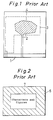
- Fig. 1 is a plan view of a conventional segment-type liquid crystal display device 1.
- a segment side transparent electrode (a portion surrounded by a solid line) 2 and a common side transparent electrode (a portion surrounded by a broken line) 3 are opposing each other forms a display area 4 which is a multiple free choice shape.
- the area outside the display area 4 is a non-lighting area wherein, at least, one of the segment side transparent electrode 2 or the common side transparent electrode 3 is absent.
- an area wherein the voltage is applied between a pair of transparent electrodes forms a black display (light interruption display) and an area wherein the voltage is not applied between a pair of transparent electrodes (hereinafter referred to as an OFF area) forms a white display (light transmission display);
- an ON area an area wherein the voltage is applied between a pair of transparent electrodes
- an OFF area an area wherein the voltage is not applied between a pair of transparent electrodes
- the black display is always formed in a white background color and the white display is not formed in a black background color.
- the white display is formed in the ON area, and the black display is formed in the OFF area, the white display is always formed in the black background color and the black display can not be formed in the white background color.
- a so-called double TN (twisted nematic) structure or a double STN (super twisted nematic) structure wherein liquid crystal display elements are piled in two layers and one liquid crystal display element is used for negative-positive inversion, may be a means to solve the aforesaid problems, such problems as increase in manufacturing cost, weight and thickness of the liquid crystal display device are newly encountered.
- a multiple nesting shape display in which, for example, a white area 7 is in a black background color area 6, and furthermore, black characters, for example, "characters and figures" are displayed therein, though it is, in principle, possible to solve the problem by providing, in the double TN structure, an electrode in one liquid crystal display element for negative-positive inversion, and mixing the negative display and positive display in the other liquid crystal display element, such problems as positioning accuracy of the liquid crystal display element and a discrepancy of displayed shape due to a parallax based on the thickness of the liquid crystal display element when looking obliquely may newly occur.
- a segment electrode formed on the segment side transparent substrate and a common electrode formed on the common side transparent substrate are formed so as to be overlapped when the two transparent substrates are arranged oppositely.
- the overlapped portion forms a display area.
- a plurality of color filters of different colors on the liquid crystal layer side surface of either of a pair of transparent substrates constituting the liquid crystal display device, and forming, for example, the segment side transparent electrodes which correspond to each color filter in the display area, and moreover, respectively connecting the segment electrodes which are formed in correspondence to the color filters of same color electrically, a color display can be realized.
- Fig. 3 is an enlarged plan view of a segment side transparent substrate 11 in a conventional color liquid crystal display device.
- three kinds of color filters for example, a red filter R, a green filter G and a blue filter B, formed into a fine rectangular shape are formed.
- a first segment electrode 12 is formed and in an area corresponding to the red filter R, a second segment electrode 13 is formed. Accordingly, when the first segment electrode 12 is brought in an ON state (voltage applied state), the area corresponding to the blue filter B exhibits the ON state, and when the second segment electrode 13 is brought in an ON state, the area corresponding to the red filter R exhibits the ON state.
- a common electrode is formed in the area including, at least, the first and second segment electrodes 12, 13.
- a so-called normally white display in which light is transmitted when the voltage is not applied, can be effected. Accordingly, in a non-voltage applied state, a white color is displayed as the background color in the liquid crystal display device.
- the first segment electrode 12 is brought in the ON state, an orientation of liquid crystal molecules of a liquid crystal layer corresponding to the color filter B is changed to interrupt the light. As a result, a yellow color is displayed in the display area by mixture of the red and green colors.
- first, second and third segment electrodes 14, 15, 16 In order to display any color among eight colors (white, cyan, magenta, yellow, blue, green, red and black) by combining the three colors, red, green and blue, first, second and third segment electrodes 14, 15, 16 must be formed for each of the three kinds of color filters R, G and B as shown in Fig. 4, and the first, second and third segment electrodes 14, 15, 16 must be driven separately, necessitating three signal lines for applying the voltage to each of the segment electrodes.
- the width of a signal line 16a sequentially connecting the third segment electrode 16 must be made extremely thinner. This is not possible because a resistance value becomes extremely high in a wiring method using an ordinary transparent conductive film.
- the color filter is selected at 80 micron width and 300 micron length. Interval between respective color filters is 30 micron, and a surface resistance value of the transparent electrode (ITO: indium tin oxide) is selected at about 40 ⁇ / ⁇ .
- ITO indium tin oxide
- the width of transparent electrode becomes 10 micron
- the interval between the transparent electrodes becomes 5 micron
- the resistance of several color filters becomes 10 to 30 times of 1.2 k ⁇ . Accordingly, it is hardly possible to drive electrically because of the high resistance value of the transparent electrode.
- the transparent electrode of 10 micron width on the transparent substrate of 30 cm to 45 cm square at the interval of 5 micron it is very difficult to pattern the transparent electrode of 10 micron width on the transparent substrate of 30 cm to 45 cm square at the interval of 5 micron.
- the four kinds of color displays are effected by the electrode arrangement and wire connection as shown in Fig. 3.
- the liquid crystal display device which is set, for example in the normally white display, four colors of magenta, blue, red and black can not be displayed.
- the kinds of display colors are restricted, and hence the display is not diverse.
- the present invention provides a segment-type color liquid crystal display device comprising a pair of light transmissible substrates with a liquid crystal layer sandwiched therebetween, first and second segment electrodes formed on the liquid crystal layer side of one of said substrates, and first and second common electrodes formed on the liquid crystal layer side of the other of said substrates, wherein the first common electrode opposes the whole of the second segment electrode and a portion only of the first segment electrode, and the second common electrode opposes the remaining portion of the first segment electrode, so as to define three distinct areas of the display whose display states are independently controllable, the display device further comprising a plurality of color filters of three different colors formed on one of said pair of substrates, the color filters of three different colors arranged in respective correspondence with said three distinct areas.
- the first segment electrode is formed corresponding to, for example, the red color filter among three kinds of color filters of red, green and blue
- the second segment electrode is formed corresponding to, for example, the green and blue color filters.
- the first common electrode is formed corresponding, for example, to the blue color filter
- the second common electrode is formed corresponding to the red and green color filters.
- the ON state (voltage applied state)/OFF state (no voltage applied state) of the liquid crystal layer corresponding to the color filters of red, green and blue can be set optionally, and by combination of the three colors, red, green and blue, the color display of eight colors in the display area is possible.
- the transparent electrode provided separately for each color filter it is not necessary for the transparent electrode provided separately for each color filter to be formed only on one light transmissible substrate as described in the description of the prior art.
- a precise patterning technique is not required and the segment side transparent electrode and the common side transparent electrode can be formed on the light transmissible substrates by the conventional patterning technique.
- three colors of red, green and blue can be optionally combined to display eight colors. Thereby, diversity of display of the liquid crystal display device can be considerably improved.
- Fig. 5 is a cross-sectional view of a color liquid crystal display device 51 according to a first embodiment of the invention
- Fig. 6 is an enlarged plan view of a transparent substrate 52
- Fig. 7 is an enlarged plan view of a transparent substrate 53.
- the color liquid crystal display device 51 includes the pair of transparent substrates or light transmissible substrates 52, 53.
- first and second segment electrodes 54, 55 are formed on one surface of the transparent substrate 52.
- the first segment electrode 54 is formed in an area corresponding to one of three color filters to be described later, for example, a red filter R.
- the second segment electrode 55 is formed in an area corresponding to two color filters other than the one corresponding to the first segment electrode 54, in this case, to a green filter G and a blue filter B.
- an organic orientation film 56 such as polyimide resin is formed.
- the color filter 58 is constituted by the three color filters (red filter R, green filter G and blue filter B) and black light interrupting layers BL formed between the filters.
- the color filters R, G, B are selected at the width and length of, for example, 80 micron and 300 micron. Intervals between the color filters are selected at 30 micron.
- first and second common electrodes 59, 60 are formed on the color filter 58.
- the first common electrode 59 is formed in an area corresponding to, among the three color filters, either of the color filters other than the one corresponding to the first segment electrode 54, in this embodiment, to the blue filter B.
- the second common electrode 60 is formed in an area corresponding to the two color filters other than the one corresponding to the first common electrode 59, in this case, to the red filter R and the green filter G.
- an organic orientation film 57 such as polyimide resin is formed.
- the transparent substrates 52, 53 are arranged such that the surfaces on which the organic orientation films 56, 57 are respectively formed face each other.
- a liquid crystal layer 61 is interposed between the transparent substrates 52, 53 and sealed by means of sealing members 62.
- the thickness of the liquid crystal layer 61 is selected at 4 micron to 30 micron.
- polarizing plates 63, 64 are respectively disposed on opposite side surfaces of the liquid crystal layer 61 side of the transparent substrates 52, 53.
- the polarizing plates 63, 64 are arranged to form, for example, a cross polarization.
- the color liquid crystal display device 51 shown in Fig. 5 though it is constructed in order of the transparent substrate 53 - color filter 58 - first and second common electrodes 59, 60 - orientation film 57, it may be constructed in order of the transparent substrate 53 - first and second common electrodes 59, 60 - color filter 58 - orientation film 57, and moreover of the transparent substrate 53 - color filter 58 - top-coat layer (transparent insulating layer) - first and second common electrodes 59, 60 - orientation film 57. Meanwhile, the color filter 58 may be formed on the transparent substrate 52.
- the combination of the electrodes and the corresponding filters is not limited thereto.
- Fig. 8 is a block diagram showing an electrical configuration of the color liquid crystal display device 51.
- a back light 69 is disposed on the opposite side of the transparent substrate 53 of the polarizing plate 64.
- the back light 69 is constituted by a reflecting case 65 and CCFT 66 of a cold cathode tube.
- a unifying light transmissible plate 67 for producing a uniform source of light and a light transmissible plate 68 consisting of a milk-white plastic, and the like are disposed.
- Light from the CCFT 66 is supplied to the color liquid crystal display device 51, and its transmission/interruption is controlled to display a predetermined display area in desired colors, by applying the square wave voltage of positive polarity or negative polarity selectively to the first and second segment electrodes 54, 55 and the first and second common electrodes 59, 60.
- the square wave voltage of positive polarity from an inverter power source 71 is applied to terminals SEG1, SEG2, COM1 and COM2 of the color liquid crystal display device 51, via a driving circuit 75.
- the driving circuit 75 comprises amplifier 72, 74, a phase inverter 73 including an amplifier, and polarity inverting switches SW11 to SW14.
- polarity inverting switches SW11 to SW14 when signal is inputted from one terminal, it is outputted as it is, and when signal is inputted from the other terminal, it is outputted with its polarity inverted.
- all of the polarity inverting switches are assumed to be connected in the same direction.
- the square wave voltage of positive polarity from the inverter power source 71 is given to the terminal SEG1 connected to the first segment electrode 54 via the polarity inverting switch SW11, to the terminal SEG2 connected to the second segment electrode 55 via the amplifier 72 and the polarity inverting switch SW12, to the terminal COM1 connected to the first common electrode 59 via the phase inverter 73 and the polarity inverting switch SW13, and further to the terminal COM2 connected to the second common electrode 60 via the phase inverter 73, amplifier 74 and polarity inverting switch SW14.
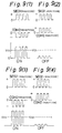
- Figs. 9(1) to 9(4) are views showing applied voltage waveforms applied to respective electrodes of the color liquid crystal display device 51.
- Figs. 9(1) and 9(2) show the applied voltage waveforms applied to the area corresponding to the red color filter R.
- the square wave voltage of positive polarity is applied to the terminal SEG1 (first segment electrode 54), and the square wave voltage of negative polarity is applied to the terminal COM2 (second common electrode 60). Accordingly, by addition of the square wave voltages of positive polarity and negative polarity, the voltage exceeding the threshold voltage Vth is applied to a liquid crystal layer corresponding to the color filter R, thus the ON state is set.
- Figs. 9(3) and 9(4) show the applied voltage waveforms applied to the liquid crystal layer in the area corresponding to the green color filter G.
- the square wave voltage of positive polarity is applied to the terminal SEG2 (second segment electrode 55), and the square wave voltage of negative polarity is applied to the terminal COM2 (second common electrode 60).
- the voltage exceeding the threshold voltage Vth is applied to the liquid crystal layer, thus the ON state is set.
- the square wave voltage of positive polarity is applied to the terminal COM2 by connecting the polarity inverting switch SW14 inversely.
- the voltage not exceeding the threshold voltage Vth is applied to the liquid crystal layer corresponding to the green color filter G, thus the OFF state is set.
- the voltage exceeding the threshold voltage Vth is applied to the liquid crystal layer in the area corresponding to the blue color filter B, thus the ON state is set.
- the polarity inverting switching SW13 inversely to apply the square wave voltage of positive polarity to the terminal COM1
- the voltage lower than the threshold voltage Vth is applied to the liquid crystal layer, thus the OFF state is set.
- electrodes can be formed respectively on the transparent substrates 52, 53 by the conventional transparent electrode patterning technique, and ON/OFF control of the areas corresponding to the color filters R, G, B can be performed separately.
- light colors can be displayed in the color liquid crystal display device 51 by optionally combining the three colors of red, green and blue.
- diversity of display of the color liquid crystal display device 51 is improved considerably.
- the transparent electrode patterning on the transparent substrates 52, 53 can be effected by the conventional manufacturing technique, thus an increase in cost can be prevented and the color liquid crystal display device 51 can be manufactured at low cost.
- Fig. 10 is a cross-sectional view showing a second embodiment of the invention. This embodiment is similar to the first embodiment, thus like or corresponding parts are designated by like reference characters.
- the second embodiment is characterized by providing the color filter 58 on the transparent substrate 52. This embodiment involves the same effects as aforementioned.
Landscapes
- Physics & Mathematics (AREA)
- Engineering & Computer Science (AREA)
- General Physics & Mathematics (AREA)
- Chemical & Material Sciences (AREA)
- Crystallography & Structural Chemistry (AREA)
- Theoretical Computer Science (AREA)
- Nonlinear Science (AREA)
- Computer Hardware Design (AREA)
- Optics & Photonics (AREA)
- Mathematical Physics (AREA)
- Geometry (AREA)
- Liquid Crystal (AREA)
- Devices For Indicating Variable Information By Combining Individual Elements (AREA)
Applications Claiming Priority (5)
| Application Number | Priority Date | Filing Date | Title |
|---|---|---|---|
| JP253434/90 | 1990-09-21 | ||
| JP25343390A JPH04131893A (ja) | 1990-09-21 | 1990-09-21 | 液晶表示装置 |
| JP2253434A JPH04131828A (ja) | 1990-09-21 | 1990-09-21 | カラー液晶表示装置 |
| JP253433/90 | 1990-09-21 | ||
| EP91300029A EP0476797B1 (de) | 1990-09-21 | 1991-01-02 | Flüssigkristallanzeigeeinrichtung |
Related Parent Applications (1)
| Application Number | Title | Priority Date | Filing Date |
|---|---|---|---|
| EP91300029.5 Division | 1991-01-02 |
Publications (2)
| Publication Number | Publication Date |
|---|---|
| EP0681283A2 true EP0681283A2 (de) | 1995-11-08 |
| EP0681283A3 EP0681283A3 (de) | 1995-12-27 |
Family
ID=26541192
Family Applications (2)
| Application Number | Title | Priority Date | Filing Date |
|---|---|---|---|
| EP95201844A Withdrawn EP0681283A3 (de) | 1990-09-21 | 1991-01-02 | Flüssigkristallanzeigeeinrichtung. |
| EP91300029A Expired - Lifetime EP0476797B1 (de) | 1990-09-21 | 1991-01-02 | Flüssigkristallanzeigeeinrichtung |
Family Applications After (1)
| Application Number | Title | Priority Date | Filing Date |
|---|---|---|---|
| EP91300029A Expired - Lifetime EP0476797B1 (de) | 1990-09-21 | 1991-01-02 | Flüssigkristallanzeigeeinrichtung |
Country Status (4)
| Country | Link |
|---|---|
| US (1) | US5155476A (de) |
| EP (2) | EP0681283A3 (de) |
| KR (1) | KR920006786A (de) |
| DE (1) | DE69119009T2 (de) |
Families Citing this family (10)
| Publication number | Priority date | Publication date | Assignee | Title |
|---|---|---|---|---|
| JPH07109544B2 (ja) * | 1991-05-15 | 1995-11-22 | インターナショナル・ビジネス・マシーンズ・コーポレイション | 液晶表示装置並びにその駆動方法及び駆動装置 |
| KR100448052B1 (ko) * | 1997-12-23 | 2004-12-03 | 비오이 하이디스 테크놀로지 주식회사 | 액정표시장치의데이터신호제어회로 |
| WO2000058796A1 (en) * | 1999-03-25 | 2000-10-05 | Citizen Watch Co., Ltd. | Watch with liquid crystal display panel |
| WO2000058780A1 (fr) * | 1999-03-25 | 2000-10-05 | Citizen Watch Co., Ltd. | Panneau a cristaux liquides |
| JP2001159881A (ja) * | 1999-12-02 | 2001-06-12 | Nec Corp | 液晶表示コントローラ並びに液晶表示装置 |
| JP2001326390A (ja) | 2000-05-18 | 2001-11-22 | Rohm Co Ltd | 裏面発光チップ型発光素子およびそれに用いる絶縁性基板 |
| US20040217921A1 (en) | 2003-04-30 | 2004-11-04 | Eastman Kodak Company | Display having positive and negative operation modes addressable in matrix fashion |
| US8054244B2 (en) * | 2004-12-31 | 2011-11-08 | Industrial Technology Research Institute | Method and apparatus for driving multi-segment display device |
| US8885139B2 (en) * | 2005-01-21 | 2014-11-11 | Johnson & Johnson Vision Care | Adaptive electro-active lens with variable focal length |
| US8228264B2 (en) * | 2007-03-28 | 2012-07-24 | Solomon Systech Limited | Segment driving method and system for a bistable display |
Family Cites Families (13)
| Publication number | Priority date | Publication date | Assignee | Title |
|---|---|---|---|---|
| US3647280A (en) * | 1969-11-06 | 1972-03-07 | Rca Corp | Liquid crystal display device |
| US4137524A (en) * | 1977-09-28 | 1979-01-30 | Optel Corporation | Reversible printing display |
| JPS55164616A (en) * | 1979-06-09 | 1980-12-22 | Yoshitoshi Iwamoto | Hair-growing and regenerating agent |
| US4277786A (en) * | 1979-07-19 | 1981-07-07 | General Electric Company | Multi-electrode liquid crystal displays |
| JPS5626722A (en) * | 1979-08-07 | 1981-03-14 | Nippon Steel Corp | Manufacture of manganese chloride |
| JPS5677816A (en) * | 1979-11-28 | 1981-06-26 | Sakao Yamada | Improvement of light schmidt type optical system |
| JPS56139123A (en) * | 1980-03-31 | 1981-10-30 | Sekisui Plastics Co Ltd | Method of confirming mixing state of binder and heat-insulation particle when heat insulation material is stirred |
| JPS6023485B2 (ja) * | 1980-04-18 | 1985-06-07 | 株式会社日立製作所 | 変圧器 |
| US4514920A (en) * | 1982-11-16 | 1985-05-07 | Doron Shafrir | Display module |
| US4688031A (en) * | 1984-03-30 | 1987-08-18 | Wang Laboratories, Inc. | Monochromatic representation of color images |
| CA1237836A (en) * | 1984-05-25 | 1988-06-07 | Keiichi Tokuyama | Multi-color liquid crystal display system |
| JPS63225295A (ja) * | 1987-03-14 | 1988-09-20 | シャープ株式会社 | 液晶表示装置 |
| JP2594985B2 (ja) * | 1987-11-24 | 1997-03-26 | 株式会社日立製作所 | 液晶表示素子 |
-
1991
- 1991-01-02 DE DE69119009T patent/DE69119009T2/de not_active Expired - Fee Related
- 1991-01-02 EP EP95201844A patent/EP0681283A3/de not_active Withdrawn
- 1991-01-02 EP EP91300029A patent/EP0476797B1/de not_active Expired - Lifetime
- 1991-01-07 US US07/638,081 patent/US5155476A/en not_active Expired - Lifetime
- 1991-01-12 KR KR1019910000367A patent/KR920006786A/ko not_active Ceased
Non-Patent Citations (1)
| Title |
|---|
| None |
Also Published As
| Publication number | Publication date |
|---|---|
| EP0476797A2 (de) | 1992-03-25 |
| DE69119009T2 (de) | 1996-09-19 |
| DE69119009D1 (de) | 1996-05-30 |
| EP0681283A3 (de) | 1995-12-27 |
| EP0476797A3 (en) | 1993-02-24 |
| KR920006786A (ko) | 1992-04-28 |
| US5155476A (en) | 1992-10-13 |
| EP0476797B1 (de) | 1996-04-24 |
Similar Documents
| Publication | Publication Date | Title |
|---|---|---|
| US4832457A (en) | Multipanel liquid crystal display device | |
| US4659182A (en) | Multilayered matrix liquid crystal display apparatus with particular color filter placement | |
| CN1042369C (zh) | 彩色液晶显示装置 | |
| KR100394026B1 (ko) | 액정표시장치 및 그 구동방법 | |
| EP0681283A2 (de) | Flüssigkristallanzeigeeinrichtung | |
| US7834833B2 (en) | Liquid crystal display device selectable between wide view angle display and narrow view angle display and liquid crystal display apparatus using same | |
| JPH06160910A (ja) | 表示デバイス | |
| CN108761856B (zh) | 阵列基板、液晶显示装置及驱动方法 | |
| CN109188816B (zh) | 阵列基板及其驱动方法和液晶显示装置及其驱动方法 | |
| JPH04131893A (ja) | 液晶表示装置 | |
| JPS61282823A (ja) | カラ−テレビ用液晶パネル | |
| EP0372637B1 (de) | Wiedergabeanordnung | |
| US4660935A (en) | Liquid crystal display device having electrodes shaped to compensate for positioning error | |
| US4759609A (en) | Process for the sequential control of a liquid crystal matrix display means having different optical responses in alternating and steady fields | |
| US5035488A (en) | Method of manufacturing liquid crystal devices having semiconductor switching elements | |
| JP3203841B2 (ja) | 液晶表示デバイス | |
| KR20060027812A (ko) | 액정 표시 장치 및 그 제조 방법 | |
| JPH04131828A (ja) | カラー液晶表示装置 | |
| JPH01306819A (ja) | カラー液晶表示装置 | |
| JPH08184857A (ja) | 液晶表示装置 | |
| JP2997948B2 (ja) | 多色液晶表示装置の駆動方法 | |
| EP0382534B1 (de) | Flüssigkristall-Anzeigevorrichtung vom Projektionstyp | |
| JP3007991B2 (ja) | 多色液晶表示装置の駆動方法 | |
| JPS6283721A (ja) | カラ−液晶表示素子 | |
| JPH02239230A (ja) | 液晶表示装置 |
Legal Events
| Date | Code | Title | Description |
|---|---|---|---|
| PUAI | Public reference made under article 153(3) epc to a published international application that has entered the european phase |
Free format text: ORIGINAL CODE: 0009012 |
|
| PUAL | Search report despatched |
Free format text: ORIGINAL CODE: 0009013 |
|
| AC | Divisional application: reference to earlier application |
Ref document number: 476797 Country of ref document: EP |
|
| AK | Designated contracting states |
Kind code of ref document: A2 Designated state(s): DE FR GB NL |
|
| AK | Designated contracting states |
Kind code of ref document: A3 Designated state(s): DE FR GB NL |
|
| 17P | Request for examination filed |
Effective date: 19960308 |
|
| 17Q | First examination report despatched |
Effective date: 19970429 |
|
| STAA | Information on the status of an ep patent application or granted ep patent |
Free format text: STATUS: THE APPLICATION IS DEEMED TO BE WITHDRAWN |
|
| 18D | Application deemed to be withdrawn |
Effective date: 19970910 |