EP0682338A2 - Magnetoresistive Struktur mit aneinandergrenzendem Übergang mit harter Polarisationsentwurf und mit Leitungswiderstand - Google Patents
Magnetoresistive Struktur mit aneinandergrenzendem Übergang mit harter Polarisationsentwurf und mit Leitungswiderstand Download PDFInfo
- Publication number
- EP0682338A2 EP0682338A2 EP95107179A EP95107179A EP0682338A2 EP 0682338 A2 EP0682338 A2 EP 0682338A2 EP 95107179 A EP95107179 A EP 95107179A EP 95107179 A EP95107179 A EP 95107179A EP 0682338 A2 EP0682338 A2 EP 0682338A2
- Authority
- EP
- European Patent Office
- Prior art keywords
- layer
- magnetoresistive
- magnetic
- transducer
- hard
- Prior art date
- Legal status (The legal status is an assumption and is not a legal conclusion. Google has not performed a legal analysis and makes no representation as to the accuracy of the status listed.)
- Withdrawn
Links
Images

Classifications
-
- G—PHYSICS
- G11—INFORMATION STORAGE
- G11B—INFORMATION STORAGE BASED ON RELATIVE MOVEMENT BETWEEN RECORD CARRIER AND TRANSDUCER
- G11B5/00—Recording by magnetisation or demagnetisation of a record carrier; Reproducing by magnetic means; Record carriers therefor
- G11B5/127—Structure or manufacture of heads, e.g. inductive
- G11B5/33—Structure or manufacture of flux-sensitive heads, i.e. for reproduction only; Combination of such heads with means for recording or erasing only
- G11B5/39—Structure or manufacture of flux-sensitive heads, i.e. for reproduction only; Combination of such heads with means for recording or erasing only using magneto-resistive devices or effects
- G11B5/3903—Structure or manufacture of flux-sensitive heads, i.e. for reproduction only; Combination of such heads with means for recording or erasing only using magneto-resistive devices or effects using magnetic thin film layers or their effects, the films being part of integrated structures
- G11B5/399—Structure or manufacture of flux-sensitive heads, i.e. for reproduction only; Combination of such heads with means for recording or erasing only using magneto-resistive devices or effects using magnetic thin film layers or their effects, the films being part of integrated structures with intrinsic biasing, e.g. provided by equipotential strips
Definitions
- This invention relates to magnetoresistive (MR) structures and in particular to MR structures incorporating a hard bias design with lowered resistance.
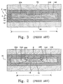
- Fig. 1 is a cross-sectional view of a conventional magnetoresistive transducer taken along a plane parallel to the Air Bearing Surface (ABS) of the device.
- the transducer generally designated by reference numeral 2, comprises a multilayer structure 4 sandwiched between a pair of shields 6A and 6B via an insulating dielectric 10.
- Shields 6A and 6B are commonly made of a ferromagnetic material with a high permeability and a low coercive force.
- the function of shields 6A and 6B, which encompass the multi-layer structure 4, is to produce a high resolution device.
- Multi-layer structure 4 includes a magnetoresistive (MR) layer 8 of soft ferromagnetic material having a low coercive force.
- MR magnetoresistive
- the soft adjacent layer 18 and the magnetoresistive layer 8 are spaced by a spacer layer 16 which is normally made of a nonmagnetic material.
- the soft adjacent layer 18 is generally formed of a soft magnetic material having a high permeability and is essentially magnetically saturated in a direction transverse to the longitudinal bias derived from the hard magnetic layer.
- a bias current is applied through electrical leads 20A and 20B which are normally made of an electrically conductive material such as Tungsten (W) or Gold (Au).
- the bias current passes through the magnetoresistive layer 8 via the hard-magnetic layers 14A and 14B.
- changes in the magnetic flux intercepted by the transducer 2 vary the electrical resistivity of the magnetoresistive layer 8.
- the current passing through the magnetoresistive layer 8 varies the resistivity and accordingly generates a varying voltage. This voltage corresponds to the information read out from the storage medium (not shown).
- the varying voltage is available at electrical leads 20A and 20B and can be fed to a sense amplifier (not shown) for amplification. It should be noted that in transducer 2, hard-magnetic layers 14A and 14B are interposed between electrical leads 20A and 20B, respectively.
- U.S. Patents 4.663,685 and 5,005,096 describe systems using a current path from connecting leads, which contains a coextensive region of longitudinal bias permanent magnet material, such as CoP and layers of CoCr, CoNiCr or CoCrPt.
- the patents describe an additional coextensive conductive layer which further increases the electrical resistance of the current path to the MR layer.
- the prior art patents exhibit higher resistance paths to the MR layer which is an undesirable condition.
- Fig. 2 shows such a transducer designated by reference numeral 22.
- hard-magnetic bias layers 24A and 24B form abutting junctions 26A and 26B, respectively, with magnetoresistive layer 8.
- Hard-magnetic layers 24A and 24B supply a more continuous longitudinal magnetic bias as well as a more direct path to the magnetoresistive layer 8, in comparison with the transducers shown in the referenced patents.
- a bias electrical current is supplied through magnetoresistive layer 8 via electrical leads 20A and 20B during the read mode.
- abutting junctions 26A and 26B are sometimes affixed with residual oxides left over from the fabrication process. These residual junction oxides do not affect the magnetic flux of the longitudinal magnetic bias, but can be detrimental to the passage of bias current, and consequently the sensed voltage. As a result, the signal-to-noise ratio can be deteriorated in some instances, and may even cause reliability problems in other instances. To rectify this shortfall, the residual oxides may be more thoroughly removed, but at the expenses of extra manufacturing steps and tighter monitoring processes. Transducers of this type can be found in United States Patent No. 5,018,037, Krounbi et al., entitled “Magnetoresistive Read Transducer Having Hard Magnetic Bias", issued May 21, 1991.
- transducer 22 is a compromise between conflicting requirements.
- the objective is to ease the fabrication of devices by relaxing manufacturing tolerances and requiring less stringent monitoring processes.
- the magnetoresistive read transducer includes a magnetoresistive layer having end regions spaced by a central active region.
- a pair of hard-magnetic layers provide the longitudinal magnetic bias to the magnetoresistive layer.
- Each of the hard-magnetic layers is disposed in contact with one of the end regions of the magnetoresistive layer.
- a pair of electrical leads provides the sense current to the magnetoresistive layer.
- Each of the electrical leads is also disposed in contact with one of the end regions of the magnetoresistive layer.
- electrical current directly passes through the central active region of the magnetoresistive layer via the electrical leads as a low electrical resistance path. Magnetic flux from the bias film renders the central MR active region in as ingle domain state.
- a transducer 32 is disposed in a magnetic head 34 having a protective shell 36.
- the protective shell 36 is preferably made of a nonmagnetic and nonconducting material, such as ceramic.
- Magnetic shields 38A-38C are preferably made of a soft magnetic material having a low coercive force and a high permeability. Examples are Permalloy (NiFe) and sendust (AlSiFe). There are also two conducting strips 46A and 46B connected to read transducer 32 for conveying sensed electrical signals to a sense amplifier (not shown).
- recording medium 42 travels in the direction 48 underneath the air bearing surface 43 of magnetic head 34, for example.
- Information stored on recording medium 42 is intercepted by transducer 32 as changes of magnetic flux. These changes of magnetic flux are converted by the transducer 32 into electrical signals at conductor strips 46A and 46B.
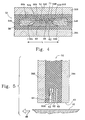
- Fig. 1 is the insulating dielectric between shields 38A-38C. However, the insulating dielectric is shown in Figs. 4 and 5.
- Figs. 4 and 5 are crosssectional views taken along lines 4-4 and 5-5, respectively, of Fig. 1.
- Insulating dielectric 50 is preferably a material which is non-magnetic and non-conducting.
- insulating dielectric 50 comprises alumina (Al2O3).
- the transducer 32 includes a magnetoresistive layer 52 formed of a soft magnetic material having a high permeability and a low coercive force. Magnetoresistive layer 52 comprises two end regions 52A and 52B spaced by a central active region 52C.
- hard-magnetic layers 54A and 54B Disposed at each of the end regions 52A and 52B are hard-magnetic layers 54A and 54B, respectively.
- hard-magnetic layers 54A and 54B are permanently magnetized and cooperatively provide a longitudinal magnetic bias for maintaining a single domain state in magnetoresistive layer 52.
- the magnetic moment for the longitudinal magnetic bias is designated by reference numeral 56.
- hard-magnetic layers 54A and 54B are disposed in abutting contact with regions 52A and 52B of magnetoresistive layer 52 through abutting junctions 58A and 58B, respectively.
- Hard-magnetic layers 54A and 54B are made of a material having a high magnetic moment and a high coercive force.
- magnetoresistive layer 52 comprises a ferromagnetic material called permalloy (NiFe), and is formed by the conventional deposition process with a thickness of between 50 to 500 Angstroms.
- a hard-magnetic layer is deposited to a thickness of between 200 to 800 Angstroms.
- Soft-magnetic layer 60 is formed of a material with a low coercive force and a high permeability.
- soft-magnetic layer 60 includes an alloy of Nickel, Iron and Rhodium (NiFeRh) and is formed by the conventional deposition process with a thickness of between 50 to 400 Angstroms.
- the spacer layer 62 comprises Tantalum (Ta) with a deposited thickness ranging from 50 to 200 Angstroms.
- electrical leads 66A and 66B formed in contact with end regions 52A and 52B of the magnetoresistive layer 52 through contact junctions 68A and 68B, respectively.
- electrical leads 66A and 66B are also disposed in contact with the hard-magnetic bias layers 54A and 54B, respectively, as shown in Fig. 4.
- Electrical leads 66A and 66B are electrical conductors and can be made from a variety of materials with high electrical conductivity. Examples are metals or various alloys including Gold (Au), Copper (Cu) and Tungsten (W).
- electrical leads are made of gold on a thin layer of about 100 Angstroms of tanatalum and are deposited by a conventional deposition process with a thickness of between 500 to 3,000 Angstroms.
- a sense current 70 is applied to electrical leads 66A and 66B (Fig. 4).
- Recording medium 42 moves in the direction 48, and accordingly, transducer 32 experiences changes in magnetic flux (Fig. 5).
- Fig. 5 These changes in magnetic flux are intercepted by the magnetoresistive layer 52 which reacts correspondingly with changes in resistivity.
- a varying voltage is generated from the sense current 70 flowing through the magnetoresistive layer 52 with varying resistivity.
- the varying voltage constitutes the electrical signals which correspond to the information read out from the recording medium 42.
- the electrical signals can be fed to a sense amplifier (not shown) via electrical leads 66A and 66B for amplification.
- soft-magnetic bias layer 60 appropriately positions magnetoresistive layer in the linear operating region, and hard-magnetic layers 66A and 66B properly suppress the Barkhausen noise.
- the output signals therefore vary substantially linearly with respect to the changes in magnetic flux emanating from the moving recording medium 42.
- electrical leads 66A and 66B are in contact with end regions 52A and 52B of magnetoresistive layer 52 through contact junctions 68A and 68B, respectively.
- electrical current 70 and longitudinal magnetic bias 56 assume somewhat separated paths.
- electrical leads are not formed in contact with the magnetoresistive layer, whereby, current and longitudinal magnetic bias are arranged to share a common path through the hard-magnetic bias layers. This is based on the belief that a shared magnetic and electrical path occupies less physical space and therefore a smaller transducer can be built as a result.
- the hard-magnetic layers and their interface junctions with the magnetoresistive layer have to be large in surface area in order to minimize the electrical resistance and to minimize the possibility of open contacts caused by the manufacturing process and possible electromigration problems caused by high density current forced through the junction.
- larger surface areas for the hard-magnetic layer and their interface junctions increase the chance of magnetic discontinuity, which in turn negatively affect the magnetic reliability.
- a middle ground is very often chosen between the two extremes. For this reason, most prior art transducers are not optimally designed.
- transducer 32 of the present invention With electrical leads 66A and 66B in contact with magnetoresistive layer 52, together, they form an electrical path of low lead resistance. There is no further need for hard-magnetic layers 54A and 54B and their interface junctions with the layer 52 to be designed with large surface areas for electrical reliability concern. Consequently, lateral dimension L can be scaled down with a smaller geometry which in turn allows the recording track width on the recording medium 42 to be further reduced. A transducer with higher performance can thus be fabricated.
- the majority of the activity is substantially concentrated at the central active region 52C of the magnetoresistive layer 52.
- the extended contact junctions 68A and 68B enable current 70 to considerably pass through the active central region 52C of the magnetoresistive layer 52.
- the consequential benefit is that there is lower lead resistance for the bias current, and a better signal-to-noise ratio for the sensed voltage.
- electrical leads 66A and 66B are also disposed in contact with hard-magnetic layers 54A and 54B, respectively.
- transducer 32 need not be arranged in a manner as described in the preferred embodiment.
- transducer 32 can well be disposed between a gap formed by two shields coplanar with each other.
Landscapes
- Engineering & Computer Science (AREA)
- Manufacturing & Machinery (AREA)
- Magnetic Heads (AREA)
- Hall/Mr Elements (AREA)
Applications Claiming Priority (2)
| Application Number | Priority Date | Filing Date | Title |
|---|---|---|---|
| US242457 | 1981-03-11 | ||
| US08/242,457 US5438470A (en) | 1994-05-13 | 1994-05-13 | Magnetoresistive structure with contiguous junction hard bias design with low lead resistance |
Publications (2)
| Publication Number | Publication Date |
|---|---|
| EP0682338A2 true EP0682338A2 (de) | 1995-11-15 |
| EP0682338A3 EP0682338A3 (de) | 1996-07-24 |
Family
ID=22914854
Family Applications (1)
| Application Number | Title | Priority Date | Filing Date |
|---|---|---|---|
| EP95107179A Withdrawn EP0682338A3 (de) | 1994-05-13 | 1995-05-11 | Magnetoresistive Struktur mit aneinandergrenzendem Übergang mit harter Polarisationsentwurf und mit Leitungswiderstand. |
Country Status (3)
| Country | Link |
|---|---|
| US (1) | US5438470A (de) |
| EP (1) | EP0682338A3 (de) |
| JP (1) | JPH0845037A (de) |
Families Citing this family (44)
| Publication number | Priority date | Publication date | Assignee | Title |
|---|---|---|---|---|
| US5712751A (en) * | 1994-03-17 | 1998-01-27 | Kabushiki Kaisha Toshiba | Magnetic sensor and magnetic recording-reproducing head and magnetic recording-reproducing apparatus using same |
| JPH0845027A (ja) * | 1994-07-29 | 1996-02-16 | Fujitsu Ltd | 磁気抵抗効果素子及びその製造方法 |
| US5896251A (en) * | 1994-12-26 | 1999-04-20 | Kabushiki Kaisha Toshiba | Magnetoresistance effect head with conductor film pair and magnetic field proving film pair disposed between substrate and magnetoresistance effect film |
| JPH08221719A (ja) * | 1995-02-16 | 1996-08-30 | Tdk Corp | スピンバルブ磁気抵抗ヘッド及びその製造方法 |
| US5646805A (en) * | 1995-03-06 | 1997-07-08 | Read-Rite Corporation | Magnetoresistive read transducer with partially abutted junctions |
| US5838521A (en) * | 1995-04-17 | 1998-11-17 | Read-Rite Corporation | Magnetoresistive transducer having laminated magnetic shields |
| US5646051A (en) * | 1995-05-05 | 1997-07-08 | Nec Research Institute, Inc. | Process for forming a magnetoresistive sensor for a reading head |
| KR100234176B1 (ko) * | 1995-06-30 | 1999-12-15 | 이형도 | 자기 저항소자 및 그 제조방법 |
| JP3635504B2 (ja) * | 1995-08-31 | 2005-04-06 | 富士通株式会社 | 磁気抵抗効果ヘッドとその製造方法及び磁気記録装置 |
| US5754376A (en) * | 1995-09-12 | 1998-05-19 | Hitachi Metals, Ltd. | Magnetoresistive head with hard magnetic bias |
| US5818684A (en) * | 1995-09-13 | 1998-10-06 | Kabushiki Kaisha Toshiba | Shield type magnetoresistive head arranged for weakening of a galvano-current magnetic field |
| EP0770991A3 (de) | 1995-10-26 | 1998-05-20 | Read-Rite Corporation | Dünnfilmmagnetoresistiver Kopf mit aneinandergrenzendem Übergang |
| US5622874A (en) * | 1995-12-14 | 1997-04-22 | Nec Research Institute, Inc. | Process for forming a magnetoresistive sensor for a read/write head |
| US6545847B2 (en) | 1996-02-14 | 2003-04-08 | Hitachi, Ltd. | Magnetoresistive effect head |
| US5936810A (en) * | 1996-02-14 | 1999-08-10 | Hitachi, Ltd. | Magnetoresistive effect head |
| SG47214A1 (en) * | 1996-03-14 | 1998-03-20 | Sony Corp | Thin-film magnetic head |
| US5708358A (en) * | 1996-03-21 | 1998-01-13 | Read-Rite Corporation | Spin valve magnetoresistive transducers having permanent magnets |
| US5926348A (en) * | 1996-08-28 | 1999-07-20 | Yamaha Corporation | Magnetoresistive head having a magnetoresistive element with bent portions located at points of high longitudinal bias magnetic field intensity |
| US5739990A (en) * | 1996-11-13 | 1998-04-14 | Read-Rite Corporation | Spin-valve GMR sensor with inbound exchange stabilization |
| JP3455037B2 (ja) * | 1996-11-22 | 2003-10-06 | アルプス電気株式会社 | スピンバルブ型薄膜素子、その製造方法、及びこのスピンバルブ型薄膜素子を用いた薄膜磁気ヘッド |
| US5867889A (en) * | 1997-04-01 | 1999-02-09 | International Business Machines Corporation | Double self-aligned insulated contiguous junction for flux-guided-MR or yoke-MR head applications |
| US6040962A (en) * | 1997-05-14 | 2000-03-21 | Tdk Corporation | Magnetoresistive element with conductive films and magnetic domain films overlapping a central active area |
| US6392840B1 (en) | 1997-12-08 | 2002-05-21 | International Business Machines Corporation | Planarized side by side design of an inductive writer and single metallic magnetoresistive reader |
| US6462920B1 (en) | 1998-12-23 | 2002-10-08 | Read-Rite Corporation | Method and system for reducing MR head instability |
| US6583971B1 (en) * | 1999-03-09 | 2003-06-24 | Sae Magnetics (Hk) Ltd. | Elimination of electric-pop noise in MR/GMR device |
| US6198608B1 (en) | 1999-03-18 | 2001-03-06 | Read-Rite Corporation | MR sensor with blunt contiguous junction and slow-milling-rate read gap |
| KR100608167B1 (ko) * | 1999-07-07 | 2006-08-02 | 후지쯔 가부시끼가이샤 | 자기저항 효과형 헤드, 자기저항 효과형 헤드 제조 방법,및 정보 재생 장치 |
| US6139906A (en) * | 1999-10-07 | 2000-10-31 | Veeco Instruments, Inc. | Methods of depositing multilayer thin films |
| US6344953B1 (en) | 2000-03-08 | 2002-02-05 | Seagate Technology, Llc | Magnetoresistive read sensor using overlaid leads with insulating current guide layer |
| JP2001312803A (ja) * | 2000-04-28 | 2001-11-09 | Fujitsu Ltd | 磁気ヘッド及び磁気ヘッドの製造方法 |
| JP3260741B1 (ja) * | 2000-08-04 | 2002-02-25 | ティーディーケイ株式会社 | 磁気抵抗効果装置およびその製造方法ならびに薄膜磁気ヘッドおよびその製造方法 |
| US6813121B2 (en) | 2000-11-30 | 2004-11-02 | Hitachi Global Storage Technologies Netherlands, B.V. | Magnetic transducer with multilayer conductive leads including a tantalum layer, a chromium layer and a rhodium layer |
| JP3583079B2 (ja) | 2001-03-26 | 2004-10-27 | 株式会社東芝 | 磁気抵抗効果素子、磁気ヘッド、磁気再生装置及び磁気記憶装置 |
| JP3593320B2 (ja) * | 2001-04-20 | 2004-11-24 | アルプス電気株式会社 | 磁気検出素子及びその製造方法 |
| JP3284130B1 (ja) | 2001-04-25 | 2002-05-20 | ティーディーケイ株式会社 | 磁気抵抗効果装置およびその製造方法、薄膜磁気ヘッドおよびその製造方法、ヘッドジンバルアセンブリならびにハードディスク装置 |
| JP3260740B1 (ja) | 2001-04-25 | 2002-02-25 | ティーディーケイ株式会社 | 磁気抵抗効果装置の製造方法および薄膜磁気ヘッドの製造方法 |
| JP3877985B2 (ja) * | 2001-08-15 | 2007-02-07 | 富士通株式会社 | 磁気抵抗ヘッド及びその製造方法 |
| US7107667B2 (en) * | 2001-11-01 | 2006-09-19 | Tdk Corporation | Method for fabricating thin film magnetic head |
| US6751070B2 (en) | 2001-11-01 | 2004-06-15 | Tdk Corporation | Thin film magnetic head and method for fabricating the same |
| US6982855B2 (en) * | 2002-05-27 | 2006-01-03 | Tdk Corporation | Magnetoresistive head having layer structure between free and lead layers with layer structure including fixed magnetization layer |
| US7075761B2 (en) * | 2002-08-27 | 2006-07-11 | Hitachi Global Storage Technologies Netherlands B.V. | Lead-defined and shaped magnetic sensor |
| US7227726B1 (en) | 2002-11-12 | 2007-06-05 | Storage Technology Corporation | Method and system for providing a dual-stripe magnetoresistive element having periodic structure stabilization |
| US7116526B2 (en) * | 2002-11-22 | 2006-10-03 | International Business Machines Corporation | Lead overlay sensor with improved current path |
| JP2008159205A (ja) * | 2006-12-26 | 2008-07-10 | Fujitsu Ltd | 記憶装置、記憶装置用ヘッドの異常検出方法、異常検出プログラム |
Family Cites Families (15)
| Publication number | Priority date | Publication date | Assignee | Title |
|---|---|---|---|---|
| DE2835459A1 (de) * | 1978-08-12 | 1980-02-28 | Vacuumschmelze Gmbh | Federndes abschirmelement, insbesondere fuer magnetbandkassetten |
| US4639806A (en) * | 1983-09-09 | 1987-01-27 | Sharp Kabushiki Kaisha | Thin film magnetic head having a magnetized ferromagnetic film on the MR element |
| US4663684A (en) * | 1984-01-27 | 1987-05-05 | Hitachi, Ltd. | Magnetic transducer using magnetoresistance effect |
| US4663685A (en) * | 1985-08-15 | 1987-05-05 | International Business Machines | Magnetoresistive read transducer having patterned longitudinal bias |
| US4803580A (en) * | 1987-02-17 | 1989-02-07 | Magnetic Peripherals Inc. | Double-gap magnetoresistive head having an elongated central write/shield pole completely shielding the magnetoresistive sensor strip in the read gap |
| US5005096A (en) * | 1988-12-21 | 1991-04-02 | International Business Machines Corporation | Magnetoresistive read transducer having hard magnetic shunt bias |
| JP2728487B2 (ja) * | 1989-02-08 | 1998-03-18 | 株式会社日立製作所 | 録再分離複合型磁気ヘッド |
| US5018037A (en) * | 1989-10-10 | 1991-05-21 | Krounbi Mohamad T | Magnetoresistive read transducer having hard magnetic bias |
| JPH0434713A (ja) * | 1990-05-30 | 1992-02-05 | Sony Corp | 磁気抵抗効果型薄膜ヘッド |
| US5270893A (en) * | 1990-10-29 | 1993-12-14 | Sony Corporation | Specific core structure in a magneto-resistance head |
| JPH05258246A (ja) * | 1992-01-21 | 1993-10-08 | Internatl Business Mach Corp <Ibm> | 磁気抵抗読取りトランスジューサ |
| US5285339A (en) * | 1992-02-28 | 1994-02-08 | International Business Machines Corporation | Magnetoresistive read transducer having improved bias profile |
| JP2620500B2 (ja) * | 1992-10-02 | 1997-06-11 | インターナショナル・ビジネス・マシーンズ・コーポレイション | 磁気抵抗センサ及びその製造方法 |
| JP2576751B2 (ja) * | 1993-02-22 | 1997-01-29 | 日本電気株式会社 | 磁気抵抗効果ヘッド |
| DE69420789T2 (de) * | 1993-07-13 | 2000-04-27 | International Business Machines Corp., Armonk | Magnetoresistiver Lesewandler |
-
1994
- 1994-05-13 US US08/242,457 patent/US5438470A/en not_active Expired - Lifetime
-
1995
- 1995-05-11 EP EP95107179A patent/EP0682338A3/de not_active Withdrawn
- 1995-05-15 JP JP7115867A patent/JPH0845037A/ja active Pending
Also Published As
| Publication number | Publication date |
|---|---|
| JPH0845037A (ja) | 1996-02-16 |
| EP0682338A3 (de) | 1996-07-24 |
| US5438470A (en) | 1995-08-01 |
Similar Documents
| Publication | Publication Date | Title |
|---|---|---|
| US5438470A (en) | Magnetoresistive structure with contiguous junction hard bias design with low lead resistance | |
| US5739990A (en) | Spin-valve GMR sensor with inbound exchange stabilization | |
| US5434826A (en) | Multilayer hard bias films for longitudinal biasing in magnetoresistive transducer | |
| US4663685A (en) | Magnetoresistive read transducer having patterned longitudinal bias | |
| US5739987A (en) | Magnetoresistive read transducers with multiple longitudinal stabilization layers | |
| US5898548A (en) | Shielded magnetic tunnel junction magnetoresistive read head | |
| US5696654A (en) | Dual element magnetoresistive sensor with antiparallel magnetization directions for magnetic state stability | |
| US5838521A (en) | Magnetoresistive transducer having laminated magnetic shields | |
| EP0477941B1 (de) | Magnetkopf mit dem Effekt der Widerstandsänderung im Magnetfeld | |
| US5492720A (en) | Method of manufacturing a magnetoresistive sensor | |
| KR100331413B1 (ko) | 자기저항효과형재생헤드및그재생헤드를탑재한자기디스크장치 | |
| EP0521564B1 (de) | Dünnfilmmagnetkopf | |
| US6721147B2 (en) | Longitudinally biased magnetoresistance effect magnetic head and magnetic reproducing apparatus | |
| JPH07272225A (ja) | 磁気抵抗性ヘッド | |
| EP0521552A2 (de) | Dünnfilmmagnetkopf | |
| KR0162119B1 (ko) | 엣지가 바이어스된 자기 저항 센서 | |
| JPH0773416A (ja) | Mr形読出しトランスジューサおよびその読出し方法 | |
| EP0789250A2 (de) | Dünnschicht-Riesenmagnetoresistiver Wandler mit Fluxleitungsanordnung | |
| US6120920A (en) | Magneto-resistive effect magnetic head | |
| JPH064832A (ja) | 複合型薄膜磁気ヘッド | |
| US6028749A (en) | Magnetic head having a multilayer structure and method of manufacturing the magnetic head | |
| EP0770991A2 (de) | Dünnfilmmagnetoresistiver Kopf mit aneinandergrenzendem Übergang | |
| EP0482642B1 (de) | Zusammengesetzter magnetoresistiver Dünnfilmmagnetkopf | |
| EP0582342B1 (de) | Magnetkopf mit einer Mehrschichtstruktur und Verfahren zum Herstellen des Magnetkopfes | |
| EP0755048B1 (de) | Magnetoresistiver Aufnahmekopf |
Legal Events
| Date | Code | Title | Description |
|---|---|---|---|
| PUAI | Public reference made under article 153(3) epc to a published international application that has entered the european phase |
Free format text: ORIGINAL CODE: 0009012 |
|
| AK | Designated contracting states |
Kind code of ref document: A2 Designated state(s): DE FR GB NL |
|
| PUAL | Search report despatched |
Free format text: ORIGINAL CODE: 0009013 |
|
| AK | Designated contracting states |
Kind code of ref document: A3 Designated state(s): DE FR GB NL |
|
| 17P | Request for examination filed |
Effective date: 19960913 |
|
| 17Q | First examination report despatched |
Effective date: 19990104 |
|
| STAA | Information on the status of an ep patent application or granted ep patent |
Free format text: STATUS: THE APPLICATION IS DEEMED TO BE WITHDRAWN |
|
| 18D | Application deemed to be withdrawn |
Effective date: 20000418 |