EP0683515A1 - CMOS und Verfahren zur Herstellung desselben - Google Patents
CMOS und Verfahren zur Herstellung desselben Download PDFInfo
- Publication number
- EP0683515A1 EP0683515A1 EP95303278A EP95303278A EP0683515A1 EP 0683515 A1 EP0683515 A1 EP 0683515A1 EP 95303278 A EP95303278 A EP 95303278A EP 95303278 A EP95303278 A EP 95303278A EP 0683515 A1 EP0683515 A1 EP 0683515A1
- Authority
- EP
- European Patent Office
- Prior art keywords
- well
- region
- cmos
- impurity
- impurity layer
- Prior art date
- Legal status (The legal status is an assumption and is not a legal conclusion. Google has not performed a legal analysis and makes no representation as to the accuracy of the status listed.)
- Granted
Links
Images




Classifications
-
- H—ELECTRICITY
- H10—SEMICONDUCTOR DEVICES; ELECTRIC SOLID-STATE DEVICES NOT OTHERWISE PROVIDED FOR
- H10D—INORGANIC ELECTRIC SEMICONDUCTOR DEVICES
- H10D84/00—Integrated devices formed in or on semiconductor substrates that comprise only semiconducting layers, e.g. on Si wafers or on GaAs-on-Si wafers
- H10D84/01—Manufacture or treatment
- H10D84/0123—Integrating together multiple components covered by H10D12/00 or H10D30/00, e.g. integrating multiple IGBTs
- H10D84/0126—Integrating together multiple components covered by H10D12/00 or H10D30/00, e.g. integrating multiple IGBTs the components including insulated gates, e.g. IGFETs
- H10D84/0156—Manufacturing their doped wells
-
- H—ELECTRICITY
- H10—SEMICONDUCTOR DEVICES; ELECTRIC SOLID-STATE DEVICES NOT OTHERWISE PROVIDED FOR
- H10D—INORGANIC ELECTRIC SEMICONDUCTOR DEVICES
- H10D84/00—Integrated devices formed in or on semiconductor substrates that comprise only semiconducting layers, e.g. on Si wafers or on GaAs-on-Si wafers
- H10D84/01—Manufacture or treatment
- H10D84/0123—Integrating together multiple components covered by H10D12/00 or H10D30/00, e.g. integrating multiple IGBTs
- H10D84/0126—Integrating together multiple components covered by H10D12/00 or H10D30/00, e.g. integrating multiple IGBTs the components including insulated gates, e.g. IGFETs
- H10D84/0128—Manufacturing their channels
-
- H—ELECTRICITY
- H10—SEMICONDUCTOR DEVICES; ELECTRIC SOLID-STATE DEVICES NOT OTHERWISE PROVIDED FOR
- H10D—INORGANIC ELECTRIC SEMICONDUCTOR DEVICES
- H10D84/00—Integrated devices formed in or on semiconductor substrates that comprise only semiconducting layers, e.g. on Si wafers or on GaAs-on-Si wafers
- H10D84/01—Manufacture or treatment
- H10D84/0123—Integrating together multiple components covered by H10D12/00 or H10D30/00, e.g. integrating multiple IGBTs
- H10D84/0126—Integrating together multiple components covered by H10D12/00 or H10D30/00, e.g. integrating multiple IGBTs the components including insulated gates, e.g. IGFETs
- H10D84/0165—Integrating together multiple components covered by H10D12/00 or H10D30/00, e.g. integrating multiple IGBTs the components including insulated gates, e.g. IGFETs the components including complementary IGFETs, e.g. CMOS devices
- H10D84/0167—Manufacturing their channels
-
- H—ELECTRICITY
- H10—SEMICONDUCTOR DEVICES; ELECTRIC SOLID-STATE DEVICES NOT OTHERWISE PROVIDED FOR
- H10D—INORGANIC ELECTRIC SEMICONDUCTOR DEVICES
- H10D84/00—Integrated devices formed in or on semiconductor substrates that comprise only semiconducting layers, e.g. on Si wafers or on GaAs-on-Si wafers
- H10D84/01—Manufacture or treatment
- H10D84/0123—Integrating together multiple components covered by H10D12/00 or H10D30/00, e.g. integrating multiple IGBTs
- H10D84/0126—Integrating together multiple components covered by H10D12/00 or H10D30/00, e.g. integrating multiple IGBTs the components including insulated gates, e.g. IGFETs
- H10D84/0165—Integrating together multiple components covered by H10D12/00 or H10D30/00, e.g. integrating multiple IGBTs the components including insulated gates, e.g. IGFETs the components including complementary IGFETs, e.g. CMOS devices
- H10D84/0191—Manufacturing their doped wells
-
- H—ELECTRICITY
- H10—SEMICONDUCTOR DEVICES; ELECTRIC SOLID-STATE DEVICES NOT OTHERWISE PROVIDED FOR
- H10D—INORGANIC ELECTRIC SEMICONDUCTOR DEVICES
- H10D84/00—Integrated devices formed in or on semiconductor substrates that comprise only semiconducting layers, e.g. on Si wafers or on GaAs-on-Si wafers
- H10D84/01—Manufacture or treatment
- H10D84/02—Manufacture or treatment characterised by using material-based technologies
- H10D84/03—Manufacture or treatment characterised by using material-based technologies using Group IV technology, e.g. silicon technology or silicon-carbide [SiC] technology
- H10D84/038—Manufacture or treatment characterised by using material-based technologies using Group IV technology, e.g. silicon technology or silicon-carbide [SiC] technology using silicon technology, e.g. SiGe
-
- H—ELECTRICITY
- H10—SEMICONDUCTOR DEVICES; ELECTRIC SOLID-STATE DEVICES NOT OTHERWISE PROVIDED FOR
- H10D—INORGANIC ELECTRIC SEMICONDUCTOR DEVICES
- H10D84/00—Integrated devices formed in or on semiconductor substrates that comprise only semiconducting layers, e.g. on Si wafers or on GaAs-on-Si wafers
- H10D84/80—Integrated devices formed in or on semiconductor substrates that comprise only semiconducting layers, e.g. on Si wafers or on GaAs-on-Si wafers characterised by the integration of at least one component covered by groups H10D12/00 or H10D30/00, e.g. integration of IGFETs
- H10D84/82—Integrated devices formed in or on semiconductor substrates that comprise only semiconducting layers, e.g. on Si wafers or on GaAs-on-Si wafers characterised by the integration of at least one component covered by groups H10D12/00 or H10D30/00, e.g. integration of IGFETs of only field-effect components
- H10D84/83—Integrated devices formed in or on semiconductor substrates that comprise only semiconducting layers, e.g. on Si wafers or on GaAs-on-Si wafers characterised by the integration of at least one component covered by groups H10D12/00 or H10D30/00, e.g. integration of IGFETs of only field-effect components of only insulated-gate FETs [IGFET]
- H10D84/85—Complementary IGFETs, e.g. CMOS
- H10D84/856—Complementary IGFETs, e.g. CMOS the complementary IGFETs having different architectures than each other, e.g. high-voltage and low-voltage CMOS
Definitions
- the present invention relates to a semiconductor device and a method for manufacturing the same, and more particularly, to a CMOS which can improve punch-through characteristics of transistors formed on a well and substrate simultaneously, and a method for manufacturing the same.
- a CMOS is produced by forming PMOS and NMOS transistors on a substrate and electrically connecting them. Conventionally, after forming an N-well and P-well in the semiconductor substrate, transistors having contrasting conductivities are formed simultaneously on the wells and on the semiconductor substrate between the wells, thereby forming the CMOS.
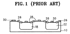
- FIG. 1 of the accompanying drawings is a cross-sectional view of a CMOS manufactured by a conventional method, where reference numeral 10 is a semiconductor substrate, reference numeral 18 is an N-well, reference numeral 22 is a P-well, reference numeral 26 is a field oxide layer, reference numeral 28 is a gate oxide layer, and reference numeral 30 is a gate electrode.
- the CMOS shown in FIG. 1 is formed by the steps of selectively doping impurities on P-type semiconductor substrate 10 to form an N-well 18 and P-well 22, performing a conventional field-oxide-layer manufacturing process to form a field oxide layer 26, forming a gate oxide layer 28 on the surface of each well and substrate, and forming a gate electrode 30 on the gate oxide layer.
- the unit size of the devices decreases, thus reducing the electrical characteristics of each device proportionally. For example, in the case of a transistor, if the gap between source and drain is reduced to increase integration, the generation rate of punch-through due to contact between source and drain depletion regions becomes higher in proportion to the gap-size reduction.
- U.S. Patent No. 4,354,307 (entitled: Method for mass producing miniature field effect transistors in high density LSI/VLSI chips; Inventor: Vinson et al.; Application No.: 99,515) teaches a method for increasing a transistor's punch-through voltage rating by selectively increasing the impurity concentration of a substrate.
- the bulk concentrations of the well and substrate which crucially influence electrical characteristics of transistors respectively formed on a well and substrate are not selectively adjusted for each transistor, it is difficult to adjust the different electric characteristics required for each transistor respectively formed on the well and substrate.
- the transistor formed on the substrate should have a high punch-through voltage by increasing the bulk concentration of the depletion region.
- the transistor formed on the well should have a low gamma ( ⁇ ) value, which represents the variation of threshold voltages due to the back-biasing.
- C OX is the capacitance of a gate oxide layer
- ⁇ s is the dielectric constant of a semiconductor substrate
- ⁇ 0 is the dielectric constant of a vacuum
- q charge quantity
- N a is the number of impurities.
- the value of qN a i.e., bulk concentration
- the bulk concentration on the well should be different from that on the substrate.
- a CMOS which comprises: first and second wells respectively formed in first and second regions of a semiconductor substrate; first and second transistors formed in the respective wells; a third transistor formed in a third region of the semiconductor substrate; a first impurity layer formed in the vicinity of the depletion region of at least one region among the first to third regions; and a second impurity layer deeper than the first impurity layer and formed in the semiconductor substrate of the region where the first impurity layer is not formed.
- the first and second wells are an N-well and P-well, respectively, and the first impurity layer is preferably formed in the vicinity of the depletion region of the third region only.
- the first and second wells are an N-well and P-well, respectively, and the first impurity layer is preferably formed in the vicinity of the depletion region of the first and second wells only.
- the first and second wells are an N-well and P-well, respectively, and the first impurity layer is preferably formed in the vicinity of the depletion region of the first well and third region only.
- the first and second wells are an N-well and P-well, respectively, and the first impurity layer is preferably formed in the vicinity of the depletion region of the second well only.
- the first and second wells are an N-well and P-well, respectively, and the first impurity layer is preferably formed in the vicinity of the depletion region of the second well and third regions only.
- the first and second wells are an N-well and P-well, respectively, and the first impurity layer is preferably formed in the vicinity of the depletion region of the first well only.
- a third impurity layer for adjusting a threshold voltage is preferably further formed in the channel region of each transistor.
- the concentration of the first and second impurity layers is preferably lower than that of the third impurity layer and is preferably higher than that of the semiconductor substrate and wells.
- a method for manufacturing a CMOS which comprises the steps of: (a) forming a first insulating layer on a semiconductor substrate; (b) removing the first insulating layer from the region for a first well to be formed thereon; (c) forming a second insulating layer on the surface of the region from which the first insulating layer is removed and forming a first well under the second insulating layer; (d) removing either of the first or second insulating layer; and (e) forming first impurity layer in the region from which the insulating layer is not removed and second impurity layer in the region from which the insulating layer is removed, respectively, by doping impurities on the whole surface of the resultant structure.
- the first impurity layer formed under the insulating layer which is not removed by the step (d) is formed in the vicinity of the depletion region of the transistor, and after the step (e), there is further provided a step of redoping impurities in the depth less than the first impurity layer on the whole surface of the resultant structure.
- the concentration of the first and second impurity layers is preferably lower than that of the third impurity layer and is preferably higher than that of the semiconductor substrate and wells.
- the first insulating layer is preferably formed in the thickness of 1,000 ⁇ 2,000 ⁇ and the second insulating layer is preferably formed in the thickness of 4,000 ⁇ 6,000 ⁇ , and at this time, the impurities are more preferably doped at the energy of 400keV-800keV.
- the step (c) there are further provided a step of removing the first insulating layer from the region for a second well to be formed thereon and a step of forming a third insulating layer on the surface of the region for a second well to be formed thereon and forming a second well under the third insulating layer.
- the first well is an N-impurity-doped well and the second well is a P-impurity-doped well.
- the second well may be formed within the first well.
- step (c) there is further provided a step of doping impurities on the region for a second well to be formed thereon to form a second well.
- the first well is an N-impurity-doped well and the second well is a P-impurity-doped well.
- the second well may be formed within the first well.
- the characteristic feature of the present invention lies in that the bulk concentration outside the depletion region does not affect the ⁇ value. That is to say, if an impurity is doped below the depletion region, the ⁇ value is unaffected.
- An impurity layer for increasing the bulk concentration in the vicinity of the depletion region is formed in a transistor requiring a high punch-through voltage in order to improve the punch-through voltage characteristic thereof. Also, an impurity layer is formed in such a depth so as to have no effect on the ⁇ value in a transistor requiring no high punch-through voltage so that the operating voltage is not affected by the back bias.
- reference numeral 10 is a semiconductor substrate
- reference numeral 18 is an N-well
- reference numeral 22 is a P-well
- reference numeral 26 is a field oxide layer
- reference numeral 28 is a gate oxide layer
- reference numeral 30 is a gate electrode
- reference numeral 100 is a first impurity layer
- reference numeral 101 is a second impurity layer
- reference numeral 102 is a third impurity layer.
- FIG. 2A is a cross-sectional view of the CMOS according to a first embodiment of the present invention.
- a first impurity layer 100 is formed in the vicinity of the depletion region of the transistor formed in the region (to be called "a third region” hereinafter) where a well is not formed.
- a third impurity layer 102 is formed in the channel region of each transistor in order to control the threshold voltage thereof.
- the first and second impurity layers 100 and 101 each have a concentration lower than the third impurity layer 102 but higher than substrate 10 and wells 18 and 22.
- the concentration of the first and second impurity layers 100 and 101 is in the range of 1.0 ⁇ 5.0E11 ions/cm2.
- the first impurity layer 100 is positioned as deeply as the depletion region is formed, for example, about 0.8-1.5 ⁇ m from the surface of the semiconductor substrate.
- first impurity layer 100 can increase the punch-through voltage of the transistor of the third-region, in which a high punch-through voltage is required.
- FIG. 2B is a cross-sectional view of the CMOS according to the second embodiment of the present invention, from which it is understood that the punch-through voltage characteristics of the transistors to be formed on the first region (N-well) 18 and second region (P-well) 22 are improved, differently from the first embodiment. Also, the first impurity layer 100 is formed in N well 18 and P well 22, and the second impurity layer 101 is formed in the third region.
- FIGS. 2C to 2F are cross-sectional views of the CMOS according to the third to sixth embodiments of the present invention, respectively.
- the CMOS of FIG. 2C is for improving punch-through voltage characteristics of the transistor to be formed on the N-well 18 and the third region
- the CMOS of FIG. 2D is for improving punch-through voltage characteristics of the transistor to be formed on the P-well 22
- the CMOS of FIG. 2E is for improving punch-through voltage characteristics of the transistor to be formed on the P-well 22 and the third region
- the CMOS of FIG. 2F is for improving punch-through voltage characteristics of the transistor to be formed on the N-well 18.
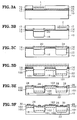
- FIGS. 3A to 3F are cross-sectional views for explaining a method for manufacturing the CMOS according to the first embodiment of the present invention.
- FIG. 3A shows a process of doping the impurity to form an N-well 22 and the process is proceeded by a first step of forming a pad oxide layer 12 and first insulating layer 14 sequentially on a semiconductor substrate 10, a second step of forming a first window 1 by performing a conventional photolithographic etching process after forming a photosensitive layer 16, e.g., a photoresist on the first insulating layer 14, and a third step of doping impurities through the first window 1.
- a photosensitive layer e.g., a photoresist
- the semiconductor substrate 10 has a specific resistance of 18 ⁇ /cm and is doped with P-type impurities.
- the pad oxide layer 12 is used as a buffer oxide layer and is formed with a thickness of 500 ⁇ 1,000 ⁇ .
- the first insulating layer 14 is a nitride layer and is formed with a thickness of 1,000 ⁇ 2,000 ⁇ , which is not limited as such but is adjusted by the doping energy of impurities and depth of the depletion region.
- the impurities are implanted using phosphorous ions at an energy of about 100keV and a concentration of 1.8E13 ions/cm2.
- FIG. 3B shows a process of completing N-well 18 and doping the impurity to form P-well and the process is preceeded by a first step of forming a second insulating layer 20 on the first region and at the same time completing the N-well 18 by performing a well drive-in process, a second step of forming a second window 2 by removing the first insulating layer in the region (second region) for a P-well to be formed thereon by performing an etching process after forming a photosensitive layer 17 for forming the P-well on the whole surface of the resultant structure, and a third step of doping impurities through the second window 2.
- the second insulating layer 20 is formed with a thickness of 4,000 ⁇ 6,000 ⁇ .
- the drive-in process is performed at 1150°C for about eight hours.
- the impurities doped through the second window 2 are boron (B) ions and are implanted at an energy of about 80keV and a concentration of 2.1E12 ions/cm2.
- FIG. 3C shows a process of completing P-well 22 and the process is proceeded such that a third insulating layer 24 is formed on the region where the impurities are doped for forming P-well and at the same time the impurities are diffused by performing a well drive-in process to complete the P-well 22.
- the drive-in process is performed at 1150°C for about eight hours.
- the N-well and P-well may be formed by respectively performing an ion-implanting process, oxidation process and drive-in processes of the N-well and the P-well with respect thereto.
- the drive-in process can proceed at the same time.
- the second insulating layer is removed after the N-well drive-in process and then the ion-implanting process is performed for forming P-well, so that the pocket P-well may be formed.
- FIG. 3D shows a process of forming first and second impurity layers 100 and 101 and the process is proceeded by a first step of removing second and third insulating layers on the respective wells and a second step of doping impurities on the whole surface of the resultant structure.
- the first impurity layer 100 is formed to be higher than the second impurity layer 101. This makes the energy of the impurities implanted with the same energy be reduced in the substrate region by the pad oxide layer and first insulating layer so that the first impurity layer becomes high.
- the impurities are ion-implanted at an energy of about 400keV ⁇ 800keV.
- the first impurity layer 100 is formed to a depth in which the depletion region is formed, i.e., about 0.8 ⁇ m ⁇ 1.5 ⁇ m into the surface of the semiconductor substrate.
- the concentration of impurities implanted for forming the first and second impurity layers is lower than an ion-implanting dosage for adjusting a threshold voltage and is higher than that of the substrate.
- the concentration corresponds to a dosage of 1.0 ⁇ 5.0E11 ions/cm2.
- FIG. 3E shows a process of forming a third impurity layer 102 for adjusting a threshold voltage and the process is proceeded by a first step of removing the pad oxide layer and first insulating layer remaining on the semiconductor substrate 10, a second step of forming a field oxide layer 26 to separate the respective well units, a third step of forming the third impurity layer 102 by doping impurities on the whole surface of the resultant structure for adjusting a threshold voltage, and a fourth step of forming a gate oxide layer 28 on the respective well and substrate.
- the impurity-implantation is carried out with boron ions at an energy of about 30keV and a dosage of about 1.7E12 ions/cm2.
- the gate oxide layer 28 is formed with a thickness of about 120 ⁇ . Of course, the thickness of gate oxide layer 28 is varied depending on the application of transistor.
- FIG. 3F shows a process of forming a gate electrode 30, which proceeds conventionally.
- the depths of the first and second impurity layers 100 and 101 of the substrate are made to be different from each other.
- the first impurity layer is formed in the source and drain depletion regions of a transistor.
- the second impurity layer is formed under the source and drain depletion regions of a transistor.
- the transistor formed on the substrate can obtain a high punch-through voltage and the transistor formed on the well can obtain an operating voltage which is not affected by the bulk concentration of the high-concentration impurity layer, thereby selectively obtaining a high punch-through voltage without a separate mask.
- the third impurity layer 102 for adjusting a threshold voltage is formed so that the threshold voltages of the respective transistors can be adjusted easily.
- FIGS. 4A to 4D are cross-sectional views for explaining a method for manufacturing the CMOS according to the second embodiment of the present invention, which is for increasing the punch-through voltage of a transistor formed on wells 18 and 22, while the first embodiment was for increasing the punch-through voltage of a transistor formed on substrate 10.
- the method of the second embodiment differs from that of the first only in that, here, first and second impurity layers 100 and 101 are formed by doping impurities after removing the first insulating layer (FIG. 4A), differently from the case of the first embodiment where first and second impurity layers are formed by doping impurities after removing the second and third insulating layers.
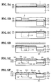
- FIGS. 5A to 5F are cross-sectional views for explaining a method for manufacturing the CMOS according to the third embodiment of the present invention, which is for selectively increasing only the punch-through voltages of transistors formed on the N-well 18 and substrate 10.
- the process is proceeded by steps of sequentially forming a pad oxide layer 12 and first insulating layer 14 on a semiconductor substrate 10, doping impurities on the region for a P-well to be formed thereon (FIG. 5A), forming a third insulating layer 24 on the region where the impurities are doped and at the same time performing the P-well 22, doping impurities on the region for an N-well to be formed thereon (FIG.
- FIGS. 5E and 5F performing a drive-in process to complete the N-well 18 (FIG. 5C), doping impurities for forming first and second impurity layers on the whole surface of the resultant structure (FIG. 5D), and repeating the steps described with respect to FIGS. 3E and 3F (FIGS. 5E and 5F).
- the third insulating layer 24 is formed on the P-well and is removed therefrom, and then impurities are doped thereon. Therefore, the first impurity layer 100 is formed in only the transistor of the N-well 18 and substrate 10, thereby increasing the punch-through voltage of the transistors formed on the N-well 18 and substrate 10.
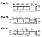
- FIGS. 6A to 6C are cross-sectional views for explaining a method for manufacturing the CMOS according to the fourth embodiment of the present invention.
- the first insulating layer formed on the N-well and substrate is removed (FIG. 6A), to increase the punch-through voltage of the transistor formed on the P-well 22.
- FIGS. 7A to 7D are cross-sectional views for explaining a method for manufacturing the CMOS according to the fifth embodiment of the present invention, which is for increasing the punch-through voltage of the transistors formed on the P-well 22 and substrate 10, differently from the third embodiment.
- P-well 22 is formed after N-well 18.
- the insulating layer is formed on N-well 18 but not on P-well 22.
- FIGS. 8A to 8C are cross-sectional views for explaining a method for manufacturing the CMOS according to the sixth embodiment of the present invention, which is for increasing only the punch-through voltage of the transistor formed on N-well 18, differently from the fourth embodiment.
- the punch-through voltage of the transistors formed on a well and/or substrate is selectively increased without a separate mask process, individual transistor characteristics can be attained even if each transistor requires mutually different characteristics.
Landscapes
- Metal-Oxide And Bipolar Metal-Oxide Semiconductor Integrated Circuits (AREA)
- Insulated Gate Type Field-Effect Transistor (AREA)
Applications Claiming Priority (2)
| Application Number | Priority Date | Filing Date | Title |
|---|---|---|---|
| KR1019940010776A KR0144959B1 (ko) | 1994-05-17 | 1994-05-17 | 반도체장치 및 제조방법 |
| KR9410776 | 1994-05-17 |
Publications (2)
| Publication Number | Publication Date |
|---|---|
| EP0683515A1 true EP0683515A1 (de) | 1995-11-22 |
| EP0683515B1 EP0683515B1 (de) | 2001-08-16 |
Family
ID=19383254
Family Applications (1)
| Application Number | Title | Priority Date | Filing Date |
|---|---|---|---|
| EP95303278A Expired - Lifetime EP0683515B1 (de) | 1994-05-17 | 1995-05-17 | Verfahren zur Herstellung einer CMOS Vorrichtung |
Country Status (5)
| Country | Link |
|---|---|
| US (1) | US6091116A (de) |
| EP (1) | EP0683515B1 (de) |
| JP (1) | JP4101313B2 (de) |
| KR (1) | KR0144959B1 (de) |
| DE (1) | DE69522139T2 (de) |
Cited By (27)
| Publication number | Priority date | Publication date | Assignee | Title |
|---|---|---|---|---|
| WO2009013531A3 (en) * | 2007-07-20 | 2009-03-19 | X Fab Semiconductor Foundries | A method of manufacturing a semiconductor device, and a semiconductor device |
| WO2012044360A1 (en) * | 2010-09-30 | 2012-04-05 | Suvolta,Inc. | Method for reducing punch-through in a transistor device |
| US8599623B1 (en) | 2011-12-23 | 2013-12-03 | Suvolta, Inc. | Circuits and methods for measuring circuit elements in an integrated circuit device |
| US8748986B1 (en) | 2011-08-05 | 2014-06-10 | Suvolta, Inc. | Electronic device with controlled threshold voltage |
| US8811068B1 (en) | 2011-05-13 | 2014-08-19 | Suvolta, Inc. | Integrated circuit devices and methods |
| US8816754B1 (en) | 2012-11-02 | 2014-08-26 | Suvolta, Inc. | Body bias circuits and methods |
| US8819603B1 (en) | 2011-12-15 | 2014-08-26 | Suvolta, Inc. | Memory circuits and methods of making and designing the same |
| US8895327B1 (en) | 2011-12-09 | 2014-11-25 | Suvolta, Inc. | Tipless transistors, short-tip transistors, and methods and circuits therefor |
| US8970289B1 (en) | 2012-01-23 | 2015-03-03 | Suvolta, Inc. | Circuits and devices for generating bi-directional body bias voltages, and methods therefor |
| US8995204B2 (en) | 2011-06-23 | 2015-03-31 | Suvolta, Inc. | Circuit devices and methods having adjustable transistor body bias |
| US9070477B1 (en) | 2012-12-12 | 2015-06-30 | Mie Fujitsu Semiconductor Limited | Bit interleaved low voltage static random access memory (SRAM) and related methods |
| US9093997B1 (en) | 2012-11-15 | 2015-07-28 | Mie Fujitsu Semiconductor Limited | Slew based process and bias monitors and related methods |
| US9112484B1 (en) | 2012-12-20 | 2015-08-18 | Mie Fujitsu Semiconductor Limited | Integrated circuit process and bias monitors and related methods |
| US9236466B1 (en) | 2011-10-07 | 2016-01-12 | Mie Fujitsu Semiconductor Limited | Analog circuits having improved insulated gate transistors, and methods therefor |
| US9268885B1 (en) | 2013-02-28 | 2016-02-23 | Mie Fujitsu Semiconductor Limited | Integrated circuit device methods and models with predicted device metric variations |
| US9319013B2 (en) | 2014-08-19 | 2016-04-19 | Mie Fujitsu Semiconductor Limited | Operational amplifier input offset correction with transistor threshold voltage adjustment |
| US9431068B2 (en) | 2012-10-31 | 2016-08-30 | Mie Fujitsu Semiconductor Limited | Dynamic random access memory (DRAM) with low variation transistor peripheral circuits |
| US9680470B2 (en) | 2011-02-18 | 2017-06-13 | Mie Fujitsu Semiconductor Limited | Digital circuits having improved transistors, and methods therefor |
| US9710006B2 (en) | 2014-07-25 | 2017-07-18 | Mie Fujitsu Semiconductor Limited | Power up body bias circuits and methods |
| US9786703B2 (en) | 2013-05-24 | 2017-10-10 | Mie Fujitsu Semiconductor Limited | Buried channel deeply depleted channel transistor |
| US9793172B2 (en) | 2011-05-16 | 2017-10-17 | Mie Fujitsu Semiconductor Limited | Reducing or eliminating pre-amorphization in transistor manufacture |
| US9812550B2 (en) | 2012-06-27 | 2017-11-07 | Mie Fujitsu Semiconductor Limited | Semiconductor structure with multiple transistors having various threshold voltages |
| US9865596B2 (en) | 2010-04-12 | 2018-01-09 | Mie Fujitsu Semiconductor Limited | Low power semiconductor transistor structure and method of fabrication thereof |
| US9893148B2 (en) | 2013-03-14 | 2018-02-13 | Mie Fujitsu Semiconductor Limited | Method for fabricating a transistor device with a tuned dopant profile |
| US9922977B2 (en) | 2010-06-22 | 2018-03-20 | Mie Fujitsu Semiconductor Limited | Transistor with threshold voltage set notch and method of fabrication thereof |
| US10074568B2 (en) | 2009-09-30 | 2018-09-11 | Mie Fujitsu Semiconductor Limited | Electronic devices and systems, and methods for making and using same |
| US10325986B2 (en) | 2009-09-30 | 2019-06-18 | Mie Fujitsu Semiconductor Limited | Advanced transistors with punch through suppression |
Families Citing this family (24)
| Publication number | Priority date | Publication date | Assignee | Title |
|---|---|---|---|---|
| JP4540438B2 (ja) * | 2004-09-27 | 2010-09-08 | 富士通セミコンダクター株式会社 | 半導体装置及びその製造方法 |
| US8304835B2 (en) * | 2009-03-27 | 2012-11-06 | National Semiconductor Corporation | Configuration and fabrication of semiconductor structure using empty and filled wells |
| US8569128B2 (en) | 2010-06-21 | 2013-10-29 | Suvolta, Inc. | Semiconductor structure and method of fabrication thereof with mixed metal types |
| US8404551B2 (en) | 2010-12-03 | 2013-03-26 | Suvolta, Inc. | Source/drain extension control for advanced transistors |
| US8525271B2 (en) | 2011-03-03 | 2013-09-03 | Suvolta, Inc. | Semiconductor structure with improved channel stack and method for fabrication thereof |
| US8400219B2 (en) | 2011-03-24 | 2013-03-19 | Suvolta, Inc. | Analog circuits having improved transistors, and methods therefor |
| US8748270B1 (en) | 2011-03-30 | 2014-06-10 | Suvolta, Inc. | Process for manufacturing an improved analog transistor |
| US8796048B1 (en) | 2011-05-11 | 2014-08-05 | Suvolta, Inc. | Monitoring and measurement of thin film layers |
| US8999861B1 (en) | 2011-05-11 | 2015-04-07 | Suvolta, Inc. | Semiconductor structure with substitutional boron and method for fabrication thereof |
| US8735987B1 (en) | 2011-06-06 | 2014-05-27 | Suvolta, Inc. | CMOS gate stack structures and processes |
| US8629016B1 (en) | 2011-07-26 | 2014-01-14 | Suvolta, Inc. | Multiple transistor types formed in a common epitaxial layer by differential out-diffusion from a doped underlayer |
| KR101891373B1 (ko) | 2011-08-05 | 2018-08-24 | 엠아이이 후지쯔 세미컨덕터 리미티드 | 핀 구조물을 갖는 반도체 디바이스 및 그 제조 방법 |
| US8645878B1 (en) | 2011-08-23 | 2014-02-04 | Suvolta, Inc. | Porting a circuit design from a first semiconductor process to a second semiconductor process |
| US8614128B1 (en) | 2011-08-23 | 2013-12-24 | Suvolta, Inc. | CMOS structures and processes based on selective thinning |
| US8713511B1 (en) | 2011-09-16 | 2014-04-29 | Suvolta, Inc. | Tools and methods for yield-aware semiconductor manufacturing process target generation |
| US8883600B1 (en) | 2011-12-22 | 2014-11-11 | Suvolta, Inc. | Transistor having reduced junction leakage and methods of forming thereof |
| US8877619B1 (en) | 2012-01-23 | 2014-11-04 | Suvolta, Inc. | Process for manufacture of integrated circuits with different channel doping transistor architectures and devices therefrom |
| US9093550B1 (en) | 2012-01-31 | 2015-07-28 | Mie Fujitsu Semiconductor Limited | Integrated circuits having a plurality of high-K metal gate FETs with various combinations of channel foundation structure and gate stack structure and methods of making same |
| US9406567B1 (en) | 2012-02-28 | 2016-08-02 | Mie Fujitsu Semiconductor Limited | Method for fabricating multiple transistor devices on a substrate with varying threshold voltages |
| US8863064B1 (en) | 2012-03-23 | 2014-10-14 | Suvolta, Inc. | SRAM cell layout structure and devices therefrom |
| US8637955B1 (en) | 2012-08-31 | 2014-01-28 | Suvolta, Inc. | Semiconductor structure with reduced junction leakage and method of fabrication thereof |
| US9112057B1 (en) | 2012-09-18 | 2015-08-18 | Mie Fujitsu Semiconductor Limited | Semiconductor devices with dopant migration suppression and method of fabrication thereof |
| US9041126B2 (en) | 2012-09-21 | 2015-05-26 | Mie Fujitsu Semiconductor Limited | Deeply depleted MOS transistors having a screening layer and methods thereof |
| KR102235613B1 (ko) * | 2014-11-20 | 2021-04-02 | 삼성전자주식회사 | Mos 커패시터를 구비하는 반도체 소자 |
Citations (9)
| Publication number | Priority date | Publication date | Assignee | Title |
|---|---|---|---|---|
| JPS5331978A (en) * | 1976-09-06 | 1978-03-25 | Nec Corp | Production of complementary field effect semiconductor device |
| US4354307A (en) | 1979-12-03 | 1982-10-19 | Burroughs Corporation | Method for mass producing miniature field effect transistors in high density LSI/VLSI chips |
| JPS61242064A (ja) * | 1985-04-19 | 1986-10-28 | Toshiba Corp | 相補型半導体装置の製造方法 |
| EP0336977A1 (de) * | 1987-10-08 | 1989-10-18 | Matsushita Electric Industrial Co., Ltd. | Halbleiteranordnung und verfahren zur herstellung |
| EP0358246A1 (de) * | 1988-09-09 | 1990-03-14 | Koninklijke Philips Electronics N.V. | Verfahren zum Herstellen einer Halbleiteranordnung mit einem Siliziumkörper, in dem durch Ionenimplantationen Halbleitergebiete gebildet werden |
| US5024961A (en) * | 1990-07-09 | 1991-06-18 | Micron Technology, Inc. | Blanket punchthrough and field-isolation implant for sub-micron N-channel CMOS devices |
| US5105252A (en) * | 1991-04-09 | 1992-04-14 | Samsung Electronics Co., Ltd. | Low voltage BiCMOS and high voltage BiCMOS the same substrate |
| JPH0536917A (ja) * | 1991-07-30 | 1993-02-12 | Sony Corp | 相補型半導体装置の製造方法 |
| JPH05121683A (ja) * | 1991-10-29 | 1993-05-18 | Olympus Optical Co Ltd | 相補型mos半導体装置 |
Family Cites Families (5)
| Publication number | Priority date | Publication date | Assignee | Title |
|---|---|---|---|---|
| JPS58170047A (ja) * | 1982-03-31 | 1983-10-06 | Fujitsu Ltd | 半導体装置 |
| US4716451A (en) * | 1982-12-10 | 1987-12-29 | Rca Corporation | Semiconductor device with internal gettering region |
| JPS6410656A (en) * | 1987-07-03 | 1989-01-13 | Hitachi Ltd | Complementary type semiconductor device |
| JPH05183159A (ja) * | 1992-01-07 | 1993-07-23 | Fujitsu Ltd | 半導体装置及びその製造方法 |
| JP2837821B2 (ja) * | 1994-04-15 | 1998-12-16 | インターナショナル・ビジネス・マシーンズ・コーポレイション | 半導体デバイス |
-
1994
- 1994-05-17 KR KR1019940010776A patent/KR0144959B1/ko not_active Expired - Lifetime
-
1995
- 1995-05-17 JP JP11832795A patent/JP4101313B2/ja not_active Expired - Fee Related
- 1995-05-17 EP EP95303278A patent/EP0683515B1/de not_active Expired - Lifetime
- 1995-05-17 DE DE69522139T patent/DE69522139T2/de not_active Expired - Lifetime
- 1995-05-17 US US08/443,283 patent/US6091116A/en not_active Expired - Lifetime
Patent Citations (9)
| Publication number | Priority date | Publication date | Assignee | Title |
|---|---|---|---|---|
| JPS5331978A (en) * | 1976-09-06 | 1978-03-25 | Nec Corp | Production of complementary field effect semiconductor device |
| US4354307A (en) | 1979-12-03 | 1982-10-19 | Burroughs Corporation | Method for mass producing miniature field effect transistors in high density LSI/VLSI chips |
| JPS61242064A (ja) * | 1985-04-19 | 1986-10-28 | Toshiba Corp | 相補型半導体装置の製造方法 |
| EP0336977A1 (de) * | 1987-10-08 | 1989-10-18 | Matsushita Electric Industrial Co., Ltd. | Halbleiteranordnung und verfahren zur herstellung |
| EP0358246A1 (de) * | 1988-09-09 | 1990-03-14 | Koninklijke Philips Electronics N.V. | Verfahren zum Herstellen einer Halbleiteranordnung mit einem Siliziumkörper, in dem durch Ionenimplantationen Halbleitergebiete gebildet werden |
| US5024961A (en) * | 1990-07-09 | 1991-06-18 | Micron Technology, Inc. | Blanket punchthrough and field-isolation implant for sub-micron N-channel CMOS devices |
| US5105252A (en) * | 1991-04-09 | 1992-04-14 | Samsung Electronics Co., Ltd. | Low voltage BiCMOS and high voltage BiCMOS the same substrate |
| JPH0536917A (ja) * | 1991-07-30 | 1993-02-12 | Sony Corp | 相補型半導体装置の製造方法 |
| JPH05121683A (ja) * | 1991-10-29 | 1993-05-18 | Olympus Optical Co Ltd | 相補型mos半導体装置 |
Non-Patent Citations (4)
| Title |
|---|
| PATENT ABSTRACTS OF JAPAN vol. 11, no. 88 (E - 490)<2535> 18 March 1987 (1987-03-18) * |
| PATENT ABSTRACTS OF JAPAN vol. 17, no. 325 (E - 1384) 21 June 1993 (1993-06-21) * |
| PATENT ABSTRACTS OF JAPAN vol. 17, no. 484 (E - 1426) 2 September 1993 (1993-09-02) * |
| PATENT ABSTRACTS OF JAPAN vol. 2, no. 65 (E - 34) 18 May 1978 (1978-05-18) * |
Cited By (43)
| Publication number | Priority date | Publication date | Assignee | Title |
|---|---|---|---|---|
| WO2009013531A3 (en) * | 2007-07-20 | 2009-03-19 | X Fab Semiconductor Foundries | A method of manufacturing a semiconductor device, and a semiconductor device |
| US10074568B2 (en) | 2009-09-30 | 2018-09-11 | Mie Fujitsu Semiconductor Limited | Electronic devices and systems, and methods for making and using same |
| US11887895B2 (en) | 2009-09-30 | 2024-01-30 | United Semiconductor Japan Co., Ltd. | Electronic devices and systems, and methods for making and using the same |
| US11062950B2 (en) | 2009-09-30 | 2021-07-13 | United Semiconductor Japan Co., Ltd. | Electronic devices and systems, and methods for making and using the same |
| US10325986B2 (en) | 2009-09-30 | 2019-06-18 | Mie Fujitsu Semiconductor Limited | Advanced transistors with punch through suppression |
| US10224244B2 (en) | 2009-09-30 | 2019-03-05 | Mie Fujitsu Semiconductor Limited | Electronic devices and systems, and methods for making and using the same |
| US10217668B2 (en) | 2009-09-30 | 2019-02-26 | Mie Fujitsu Semiconductor Limited | Electronic devices and systems, and methods for making and using the same |
| US9865596B2 (en) | 2010-04-12 | 2018-01-09 | Mie Fujitsu Semiconductor Limited | Low power semiconductor transistor structure and method of fabrication thereof |
| US9922977B2 (en) | 2010-06-22 | 2018-03-20 | Mie Fujitsu Semiconductor Limited | Transistor with threshold voltage set notch and method of fabrication thereof |
| WO2012044360A1 (en) * | 2010-09-30 | 2012-04-05 | Suvolta,Inc. | Method for reducing punch-through in a transistor device |
| US9680470B2 (en) | 2011-02-18 | 2017-06-13 | Mie Fujitsu Semiconductor Limited | Digital circuits having improved transistors, and methods therefor |
| US10250257B2 (en) | 2011-02-18 | 2019-04-02 | Mie Fujitsu Semiconductor Limited | Digital circuits having improved transistors, and methods therefor |
| US9985631B2 (en) | 2011-02-18 | 2018-05-29 | Mie Fujitsu Semiconductor Limited | Digital circuits having improved transistors, and methods therefor |
| US9838012B2 (en) | 2011-02-18 | 2017-12-05 | Mie Fujitsu Semiconductor Limited | Digital circuits having improved transistors, and methods therefor |
| US8811068B1 (en) | 2011-05-13 | 2014-08-19 | Suvolta, Inc. | Integrated circuit devices and methods |
| US9966130B2 (en) | 2011-05-13 | 2018-05-08 | Mie Fujitsu Semiconductor Limited | Integrated circuit devices and methods |
| US9741428B2 (en) | 2011-05-13 | 2017-08-22 | Mie Fujitsu Semiconductor Limited | Integrated circuit devices and methods |
| US9362291B1 (en) | 2011-05-13 | 2016-06-07 | Mie Fujitsu Semiconductor Limited | Integrated circuit devices and methods |
| US9793172B2 (en) | 2011-05-16 | 2017-10-17 | Mie Fujitsu Semiconductor Limited | Reducing or eliminating pre-amorphization in transistor manufacture |
| US8995204B2 (en) | 2011-06-23 | 2015-03-31 | Suvolta, Inc. | Circuit devices and methods having adjustable transistor body bias |
| US8748986B1 (en) | 2011-08-05 | 2014-06-10 | Suvolta, Inc. | Electronic device with controlled threshold voltage |
| US8963249B1 (en) | 2011-08-05 | 2015-02-24 | Suvolta, Inc. | Electronic device with controlled threshold voltage |
| US9236466B1 (en) | 2011-10-07 | 2016-01-12 | Mie Fujitsu Semiconductor Limited | Analog circuits having improved insulated gate transistors, and methods therefor |
| US8895327B1 (en) | 2011-12-09 | 2014-11-25 | Suvolta, Inc. | Tipless transistors, short-tip transistors, and methods and circuits therefor |
| US8819603B1 (en) | 2011-12-15 | 2014-08-26 | Suvolta, Inc. | Memory circuits and methods of making and designing the same |
| US8599623B1 (en) | 2011-12-23 | 2013-12-03 | Suvolta, Inc. | Circuits and methods for measuring circuit elements in an integrated circuit device |
| US9297850B1 (en) | 2011-12-23 | 2016-03-29 | Mie Fujitsu Semiconductor Limited | Circuits and methods for measuring circuit elements in an integrated circuit device |
| US8970289B1 (en) | 2012-01-23 | 2015-03-03 | Suvolta, Inc. | Circuits and devices for generating bi-directional body bias voltages, and methods therefor |
| US10217838B2 (en) | 2012-06-27 | 2019-02-26 | Mie Fujitsu Semiconductor Limited | Semiconductor structure with multiple transistors having various threshold voltages |
| US9812550B2 (en) | 2012-06-27 | 2017-11-07 | Mie Fujitsu Semiconductor Limited | Semiconductor structure with multiple transistors having various threshold voltages |
| US10014387B2 (en) | 2012-06-27 | 2018-07-03 | Mie Fujitsu Semiconductor Limited | Semiconductor structure with multiple transistors having various threshold voltages |
| US9431068B2 (en) | 2012-10-31 | 2016-08-30 | Mie Fujitsu Semiconductor Limited | Dynamic random access memory (DRAM) with low variation transistor peripheral circuits |
| US9154123B1 (en) | 2012-11-02 | 2015-10-06 | Mie Fujitsu Semiconductor Limited | Body bias circuits and methods |
| US8816754B1 (en) | 2012-11-02 | 2014-08-26 | Suvolta, Inc. | Body bias circuits and methods |
| US9093997B1 (en) | 2012-11-15 | 2015-07-28 | Mie Fujitsu Semiconductor Limited | Slew based process and bias monitors and related methods |
| US9070477B1 (en) | 2012-12-12 | 2015-06-30 | Mie Fujitsu Semiconductor Limited | Bit interleaved low voltage static random access memory (SRAM) and related methods |
| US9112484B1 (en) | 2012-12-20 | 2015-08-18 | Mie Fujitsu Semiconductor Limited | Integrated circuit process and bias monitors and related methods |
| US9268885B1 (en) | 2013-02-28 | 2016-02-23 | Mie Fujitsu Semiconductor Limited | Integrated circuit device methods and models with predicted device metric variations |
| US9893148B2 (en) | 2013-03-14 | 2018-02-13 | Mie Fujitsu Semiconductor Limited | Method for fabricating a transistor device with a tuned dopant profile |
| US9991300B2 (en) | 2013-05-24 | 2018-06-05 | Mie Fujitsu Semiconductor Limited | Buried channel deeply depleted channel transistor |
| US9786703B2 (en) | 2013-05-24 | 2017-10-10 | Mie Fujitsu Semiconductor Limited | Buried channel deeply depleted channel transistor |
| US9710006B2 (en) | 2014-07-25 | 2017-07-18 | Mie Fujitsu Semiconductor Limited | Power up body bias circuits and methods |
| US9319013B2 (en) | 2014-08-19 | 2016-04-19 | Mie Fujitsu Semiconductor Limited | Operational amplifier input offset correction with transistor threshold voltage adjustment |
Also Published As
| Publication number | Publication date |
|---|---|
| JPH07321216A (ja) | 1995-12-08 |
| DE69522139T2 (de) | 2002-04-11 |
| JP4101313B2 (ja) | 2008-06-18 |
| DE69522139D1 (de) | 2001-09-20 |
| KR0144959B1 (ko) | 1998-07-01 |
| KR950034740A (ko) | 1995-12-28 |
| EP0683515B1 (de) | 2001-08-16 |
| US6091116A (en) | 2000-07-18 |
Similar Documents
| Publication | Publication Date | Title |
|---|---|---|
| EP0683515A1 (de) | CMOS und Verfahren zur Herstellung desselben | |
| EP0661751B1 (de) | Verfahren zum Herstellen eines CMOS-Bauteil mit Hoch- und Niedrigspannungstransistoren | |
| US6548874B1 (en) | Higher voltage transistors for sub micron CMOS processes | |
| EP0387999B1 (de) | Verfahren zum Herstellen von Hochspannungs- und Niederspannungs-CMOS-Transistoren in einem einzigen integrierten Schaltungs-Chip | |
| US4784968A (en) | Process for manufacturing a semiconductor device having MIS-type field effect transistors with impurity region below the gate electrode | |
| US5897363A (en) | Shallow junction formation using multiple implant sources | |
| US5397715A (en) | MOS transistor having increased gate-drain capacitance | |
| EP0187016A2 (de) | MISFET mit niedrigdotiertem Drain und Verfahren zu seiner Herstellung | |
| EP0676810A2 (de) | Feldeffekttransistor mit isolierten Gate und Herstellungsverfahren | |
| EP0550015A1 (de) | Lateraler zweifach diffundierter Fieldeffekttransistor mit einem isolierten Gate und Verfahren zur Herstellung | |
| US20030025165A1 (en) | Buried channel pmos transistor in dual gate cmos with reduced masking steps | |
| EP0166167B1 (de) | Verfahren zur Herstellung einer Halbleiteranordnung mit p-Kanal und n-Kanal MISFETs | |
| JPH08250728A (ja) | 電界効果型半導体装置及びその製造方法 | |
| US5726476A (en) | Semiconductor device having a particular CMOS structure | |
| EP0135243B1 (de) | Verfahren zum Herstellen einer Halbleiterstruktur auf einem Substrat und danach hergestellte Halbleiteranordnung | |
| US6873021B1 (en) | MOS transistors having higher drain current without reduced breakdown voltage | |
| US5416038A (en) | Method for producing semiconductor device with two different threshold voltages | |
| US20030127694A1 (en) | Higher voltage transistors for sub micron CMOS processes | |
| US6583013B1 (en) | Method for forming a mixed voltage circuit having complementary devices | |
| US6930005B2 (en) | Low cost fabrication method for high voltage, high drain current MOS transistor | |
| Chen et al. | A high performance submicron CMOS process with self-aligned chan-stop and punch-through implants (twin-tub V) | |
| WO1999003149A1 (en) | Semiconductor device having a nitrogen bearing isolation region and process of manufacture thereof | |
| EP0468271A1 (de) | Bipolartransistor und Herstellungsverfahren | |
| US7560779B2 (en) | Method for forming a mixed voltage circuit having complementary devices | |
| US5830789A (en) | CMOS process forming wells after gate formation |
Legal Events
| Date | Code | Title | Description |
|---|---|---|---|
| PUAI | Public reference made under article 153(3) epc to a published international application that has entered the european phase |
Free format text: ORIGINAL CODE: 0009012 |
|
| AK | Designated contracting states |
Kind code of ref document: A1 Designated state(s): DE FR GB IT |
|
| 17P | Request for examination filed |
Effective date: 19960404 |
|
| 17Q | First examination report despatched |
Effective date: 19970908 |
|
| RTI1 | Title (correction) |
Free format text: METHOD OF MANUFACTURING A CMOS DEVICE |
|
| GRAG | Despatch of communication of intention to grant |
Free format text: ORIGINAL CODE: EPIDOS AGRA |
|
| GRAG | Despatch of communication of intention to grant |
Free format text: ORIGINAL CODE: EPIDOS AGRA |
|
| GRAH | Despatch of communication of intention to grant a patent |
Free format text: ORIGINAL CODE: EPIDOS IGRA |
|
| GRAH | Despatch of communication of intention to grant a patent |
Free format text: ORIGINAL CODE: EPIDOS IGRA |
|
| GRAA | (expected) grant |
Free format text: ORIGINAL CODE: 0009210 |
|
| AK | Designated contracting states |
Kind code of ref document: B1 Designated state(s): DE FR GB IT |
|
| REF | Corresponds to: |
Ref document number: 69522139 Country of ref document: DE Date of ref document: 20010920 |
|
| ET | Fr: translation filed | ||
| REG | Reference to a national code |
Ref country code: GB Ref legal event code: IF02 |
|
| PLBE | No opposition filed within time limit |
Free format text: ORIGINAL CODE: 0009261 |
|
| STAA | Information on the status of an ep patent application or granted ep patent |
Free format text: STATUS: NO OPPOSITION FILED WITHIN TIME LIMIT |
|
| 26N | No opposition filed | ||
| PGFP | Annual fee paid to national office [announced via postgrant information from national office to epo] |
Ref country code: IT Payment date: 20080526 Year of fee payment: 14 |
|
| PGFP | Annual fee paid to national office [announced via postgrant information from national office to epo] |
Ref country code: GB Payment date: 20080521 Year of fee payment: 14 |
|
| GBPC | Gb: european patent ceased through non-payment of renewal fee |
Effective date: 20090517 |
|
| PG25 | Lapsed in a contracting state [announced via postgrant information from national office to epo] |
Ref country code: GB Free format text: LAPSE BECAUSE OF NON-PAYMENT OF DUE FEES Effective date: 20090517 |
|
| PG25 | Lapsed in a contracting state [announced via postgrant information from national office to epo] |
Ref country code: IT Free format text: LAPSE BECAUSE OF NON-PAYMENT OF DUE FEES Effective date: 20090517 |
|
| PGFP | Annual fee paid to national office [announced via postgrant information from national office to epo] |
Ref country code: DE Payment date: 20140424 Year of fee payment: 20 |
|
| PGFP | Annual fee paid to national office [announced via postgrant information from national office to epo] |
Ref country code: FR Payment date: 20140521 Year of fee payment: 20 |
|
| REG | Reference to a national code |
Ref country code: DE Ref legal event code: R071 Ref document number: 69522139 Country of ref document: DE |