EP0683616B1 - Circuit de traitement de signal pour un vectorscope - Google Patents
Circuit de traitement de signal pour un vectorscope Download PDFInfo
- Publication number
- EP0683616B1 EP0683616B1 EP95303323A EP95303323A EP0683616B1 EP 0683616 B1 EP0683616 B1 EP 0683616B1 EP 95303323 A EP95303323 A EP 95303323A EP 95303323 A EP95303323 A EP 95303323A EP 0683616 B1 EP0683616 B1 EP 0683616B1
- Authority
- EP
- European Patent Office
- Prior art keywords
- signal
- burst
- chroma
- amplitude
- signals
- Prior art date
- Legal status (The legal status is an assumption and is not a legal conclusion. Google has not performed a legal analysis and makes no representation as to the accuracy of the status listed.)
- Expired - Lifetime
Links
Images



Classifications
-
- H—ELECTRICITY
- H04—ELECTRIC COMMUNICATION TECHNIQUE
- H04N—PICTORIAL COMMUNICATION, e.g. TELEVISION
- H04N17/00—Diagnosis, testing or measuring for television systems or their details
-
- G—PHYSICS
- G01—MEASURING; TESTING
- G01R—MEASURING ELECTRIC VARIABLES; MEASURING MAGNETIC VARIABLES
- G01R13/00—Arrangements for displaying electric variables or waveforms
- G01R13/20—Cathode-ray oscilloscopes
- G01R13/208—Arrangements for measuring with C.R. oscilloscopes, e.g. vectorscope
-
- G—PHYSICS
- G01—MEASURING; TESTING
- G01R—MEASURING ELECTRIC VARIABLES; MEASURING MAGNETIC VARIABLES
- G01R31/00—Arrangements for testing electric properties; Arrangements for locating electric faults; Arrangements for electrical testing characterised by what is being tested not provided for elsewhere
- G01R31/28—Testing of electronic circuits, e.g. by signal tracer
- G01R31/282—Testing of electronic circuits specially adapted for particular applications not provided for elsewhere
- G01R31/2825—Testing of electronic circuits specially adapted for particular applications not provided for elsewhere in household appliances or professional audio/video equipment
-
- H—ELECTRICITY
- H04—ELECTRIC COMMUNICATION TECHNIQUE
- H04N—PICTORIAL COMMUNICATION, e.g. TELEVISION
- H04N17/00—Diagnosis, testing or measuring for television systems or their details
- H04N17/02—Diagnosis, testing or measuring for television systems or their details for colour television signals
Definitions
- the present invention relates to a signal processing circuit for a vector scope adapted to measure the characteristics of a color video signal, and more particularly to a signal processing circuit adapted to automatically set at least one of the amplitudes represented by vectors of a burst signal and a chroma signal at a specified amplitude position on a display screen.
- the angle and amplitude of the displayed vector are related to the hue and the chroma of the color represented by the color information.
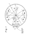
- the display screen of the vector scope is represented as shown in Fig. 1 for example.
- the vertical axis indicates the R-Y component while the horizontal axis indicates the B-Y component.
- the graduation "a" provided along the circumference of the display screen serves to indicate a phase of the chroma signal contained in the color video signal and is capable of indicating a jitter component contained in a burst signal.
- the graduation "b” provided at the leftward and of the horizontal axis serves to indicate a differential gain (DG) and a differential phase (DP) of the chroma signal.
- DG differential gain
- DP differential phase
- a lug on a front manipulation panel is manually operated to control a variable gain circuit incorporated in a signal processing circuit, watching the display screen as to align the tip end of the vector representation of a burst signal with a circumferential position of the display screen.
- a DG or DP of the chroma signal In the case that a DG or DP of the chroma signal is to be measured, it is necessary to adjust the tip end of a vector representation V c of the chroma signal to the reference point 0 (the crossing point of the horizontal axis and the circumference). Also in the case, by manually handling lugs of the manipulation panel to control a gain and phase (angle) of the chroma signal, watching the display screen, the tip end of the vector representation of a chroma signal may be adjusted to the reference point 0 of the graduation "b".
- US-3,820,156 describes a vectorscope which displays a test circle pattern without distortion on a screen.
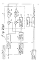
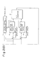
- Figs. 2(A) and 2(B) show an embodied signal processing circuit in a vector scope according to the present invention.
- reference numeral 1 designates an input terminal to which a color video signal V in is applied, 2 a manipulation panel, 3 a variable gain circuit of a voltage control type (a variable gain amplifier), 4 a sub-carrier regeneration circuit adapted to regenerate a sub-carrier signal from the color video signal V in , and 5 a digital phase shifter adapted to shift a phase of the sub-carrier signal regenerated at the circuit 4.
- Reference numeral 6 designates a demodulation circuit which receives an output signal from the variable gain circuit 3 and an output signal from the digital phase shifter 5.
- the demodulation circuit 6 includes multipliers 6 1 and 6 2 , low pass filters (LPF) 6 3 and 6 4 , amplifiers 6 5 and 6 6 having the same gain and a phase shifter 6 7 adapted to shift a phase of the output signal from the digital phase shifter 5 by -90°, and outputs vector signals R-Y and B-Y which are chrominance components of the input color video signal.
- R-Y and B-Y signal are supplied respectively to vertical and horizontal drive circuits (not shown) for driving the vertical and horizontal axes of the display screen of the vector scope so that the components of the color video signal may be displayed in terms of vector.
- reference numeral 7 designates a timing signal generation circuit which generates a timing signal T by monitoring R-Y and B-Y signals coming from the demodulation circuit 6, 8 and 9 amplitude detection circuits comprising sample and hold circuits having the same operation timing which is stipulated by the timing signal T supplied from the timing signal generation circuit 7.
- Numeral 10 designates an analog/digital (A/D) converter which converts analog signals coming from the amplitude detection circuits 8 and 9 into digital signals, and 11 a microprocessor (CPU) which controls the variable gain circuit 3 and the timing signal generation circuit 7 as well as operation of the entire vector scope.
- A/D analog/digital converter
- reference numeral 12 designates a read/write memory which stores a reference amplitude value E (b)ref at a predetermined address.
- the reference amplitude value E (b)ref is used for setting an amplitude E (b) of a vector representation of a burst signal contained in the color video signal to a predetermined amplitude corresponding to the value E (b)ref .
- the reference amplitude value E (b)ref is preferably so set that the amplitude of the vector representation coincides with the circumference of the display screen, in the course of measurement of jitter component.
- the amplitude need not necessarily coincide with the circumference but can be set at any arbitrary value if necessary. Accordingly, the value E (b)ref is changeable by operating the manipulation panel 2 by a user.
- a color video signal V in As shown in Fig. 3(A) is input to the input terminal 1, the signal is supplied to the demodulation circuit 6 via the variable gain circuit 3.
- the color video signal is also supplied to the sub-carrier regeneration circuit 4 where a sub-carrier signal is regenerated.
- the sub-carrier signal is then supplied to the demodulation circuit 6 via the phase shifter 5.
- the demodulation circuit 6 supplies, in turn, R-Y and B-Y signals as shown in Fig. 3(B). These R-Y and B-Y signals are respectively provided to the vertical and horizontal drive circuits to drive the vertical and horizontal axes of the display screen of a vector scope.
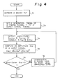
- Step S 1 In order to automatically set an amplitude of a vector representation of a burst signal to a preset size, or in order to implement a burst signal amplitude automatic setting mode (BSAAS mode), an associated key on the manipulation panel 2 is depressed at Step S 1 in Fig. 4 by a user. It is assumed that a reference amplitude value E (b)ref has been stored in the memory 12 by entering the value from the manipulation panel 2.
- the CPU11 sets the timing signal generation circuit 7 to a burst mode so that the circuit 7 generates a timing signal T as a burst timing signal T (b) at a timing corresponding to the burst signal as shown in Fig.
- Step S 3 by monitoring R-Y signal or B-Y signal provided from the demodulation circuit 6. This causes, in Step S 3 , the amplitude level of the burst signal parts R-Y (b) and B-Y (b) of R-Y and B-Y signals from the demodulation circuit 6 to be detected respectively at the amplitude detection circuits 8 and 9 and then converted by the A-D converter 10 to digital amplitude signals E R-Y(b) and E B-Y(b) .
- E R-Y(b) and E B-Y(b) are input to CPU11 where an amplitude value E (b) at that time of the vector representation of the burst signal is obtained by computing the square root of E R-Y(b) 2 + E B-Y(b) 2 in accordance with the supplied amplitude signals in Step S 4 .
- E ( b ) E R - Y ( b ) 2 + E B - Y ( b ) 2
- Step S 6 the process proceeds to Step S 6 so as to control the gain of the variable gain control 3 in such a manner as the difference ⁇ E (b) is made to be zero.
- the expression "the difference is zero” signifies simply that it is mathematically or ideally zero. However, in an actual operation, it signifies that the difference is zero in the minimum resolution which is set in advance.
- the amplitude value E (b) of the vector representation of the burst signal may be automatically set to the predetermined reference amplitude value E (b)ref .
- the signal processing circuit shown in Fig. 2 can be so constituted that the phase shift amount in the digital phase shifter 5 may be controlled by manually rotating a lug on the manipulation panel 2 in order to coincide an angle (or phase) of the vector representation of a burst signal with a specified vector angle ⁇ (b)ref such as zero (coincident with the horizontal axis), it is preferably constituted so that a so-called one-touch operation of a switch on the operational panel allows the angle to automatically coincide with the reference angle ⁇ (b)ref .
- the reference angle (or phase) ⁇ (b)ref may be previously stored in the memory 12, and a burst signal phase automatic setting mode (BSPAS mode) may performed.
- BSPAS mode burst signal phase automatic setting mode
- a signal processing circuit for a vector scope which is capable of operating in accordance with the BSAAS mode as explained above and also is capable of operating a DG/DP automatic setting mode.
- the term "DG/DP automatic setting mode” signifies such a mode as when a differential gain (DG) key or differential phase (DP) key on the manipulation panel 2 is depressed, an automatic adjustment is made so that an amplitude and/or phase of a vector representation of a chroma signal will coincide with a specified value which has been set in advance and the variation in amplitude or phase of a color video signal is displayed on the vector scope to measure the DG or DP level.
- DG/DP automatic setting mode signifies such a mode as when a differential gain (DG) key or differential phase (DP) key on the manipulation panel 2 is depressed, an automatic adjustment is made so that an amplitude and/or phase of a vector representation of a chroma signal will coincide with a specified value which has been set in advance and the variation in amplitude or phase of a color
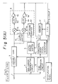
- the signal processing circuit shown in Fig. 5 further includes a synchronizing signal separation circuit 13, horizontal sweep signal generator 14, three switching circuits 15 through 17 and two amplifiers 18, 19 having different gains.
- the switching circuit 15 when the circuit is operated in the BSAAS mode, the switching circuit 15 is rendered to connect to a V/DP terminal and the switching circuits 16 and 17 are rendered to connect to V terminals respectively under a control of the CPU11 when it receives a burst signal amplitude automatic setting signal from the manipulation panel 2.
- a signal channel or path similar to that of the signal processing circuit shown in Fig. 2 is formed whereby the BSAAS mode is executed as described above in connection with Fig. 2.
- Figs. 6(A) - 6(D) illustrate waveforms of signals output from components in the signal processing circuit shown in Fig. 5 and Figs. 7(A) and 7(B) show a flow chart in the DG/DP automatic setting mode therein.
- Fig. 6(A) designates a color video signal V in of one horizontal period, which is supplied to the video signal input terminal 1
- Fig. 6(B) designates R-Y signal or (B-Y signal) which is output from the demodulation circuit 6
- Fig. 6(D) designates a horizontal sweep signal S output from the horizontal sweep signal generator 14.
- reference amplitude value E (c)ref and reference angle ⁇ (c)ref of a chroma signal are previously set and stored in specified respective addresses in the memory 12.
- Step S 7 in Fig. 7(A) when either of the DG key or the DP key on the manipulation panel is depressed, DG/DP automatic setting mode will be activated.
- Step S 8 the switching circuit 15 is controlled to connect to the V/DP terminal while the switching circuits 16 and 17 are controlled to connect to the V terminals.
- the signal generation timing of the timing signal generation circuit 7 is changed to a chroma mode so that the timing signal generation circuit 7 generates the timing signal T as the signal T (c) in the chroma signal timing interval shown in Fig. 6(C) by monitoring R-Y signal or B-Y signal output from the demodulation circuit 6.
- the amplitude detection circuits 8 and 9 By receiving the timing signal T (c) , the amplitude detection circuits 8 and 9 detect the levels of the amplitudes of the chroma signal components R-Y (c) and B-Y (c) of the R-Y signal and B-Y signal output from the demodulation circuit 6, and then the amplitude levels are converted into digital amplitude signals E R-Y(c) and E B-Y(c) , in Step S 9 .
- Step S 11 the difference ⁇ E (c) between the computed amplitude value E (c) and the reference amplitude value E (c)ref read out from the memory 12 is computed, and if the difference ⁇ E (c) is not zero, the gain of the variable gain circuit 3 is so controlled that the difference will be zero in Step S 12 .
- Step S 11 If ⁇ E (c) is attained in Step S 11 , the amplitude E (c) of the vector representation of the chroma signal has coincided with the reference amplitude value E (c)ref which has been stored in the memory 12.
- Step S 14 the switching circuits 15 through 17 are subjected to connect to DG terminals, which causes a horizontal axis of the display screen to be driven by the horizontal sweep signal S, shown in Fig. 7(D), coming from the horizontal sweep signal generator 14 and the vertical axis to be driven by an amplitude signal through the amplifier 18, whereby the amplitude level of one horizontal cycle is displayed on the display screen as shown in Fig. 8(A).
- Step S 15 the amplitudes of the R-Y (c) signal and B-Y (c) signal are detected, and in Step S 16 , using the digital amplitude signals E R-Y(c) and E B-Y(c) supplied from the A/D converter to CPU11, the phase or the angle ⁇ (c) of vector representation of the chroma signal is calculated as follows.
- ⁇ ( c ) cos -1 E B - Y ( c ) E R - Y ( c ) 2 + E B - Y ( c ) 2
- Step S 19 a DP mode is executed in Step S 19 .
- the switching circuit 15 remains to connect to the V/DP terminal while the switching circuits 16 and 17 are switched to DP terminals whereby the horizontal axis of the display screen is driven by the horizontal sweep signal S as shown in Fig. 6(D) coming from the horizontal sweep signal generator 14 and the vertical axis is driven by the R-Y signal which has been amplified by the amplifier 19. Accordingly, the phase level of the color video signal is displayed on the display screen as shown in Fig. 8(B).
- a vector representation of a burst signal contained in a color video signal may be automatically and precisely adjusted to a given amplitude. Further, a vector representation of a chroma signal can be automatically and precisely set to a given amplitude and angle (or phase). Accordingly, operability of a vector scope may be enhanced and there will not be caused any specific difference in positioning accuracy for users.
Landscapes
- Engineering & Computer Science (AREA)
- Multimedia (AREA)
- Physics & Mathematics (AREA)
- General Physics & Mathematics (AREA)
- Health & Medical Sciences (AREA)
- Biomedical Technology (AREA)
- General Health & Medical Sciences (AREA)
- Signal Processing (AREA)
- General Engineering & Computer Science (AREA)
- Processing Of Color Television Signals (AREA)
- Testing, Inspecting, Measuring Of Stereoscopic Televisions And Televisions (AREA)
Claims (5)
- Circuit de traitement de signaux d'un oscilloscope à vecteurs adapté pour afficher et mesurer des caractéristiques d'un signal vidéo couleur sur un écran, le circuit comportant un moyen à gain variable pour amplifier un signal vidéo couleur entré dans ce dernier et un circuit de démodulation pour démoduler le signal vidéo couleur amplifié en vue de fournir des premier et deuxième signaux de chrominance à des circuits d'attaque verticale et horizontale de l'écran, respectivement,
CARACTERISE EN CE QUE
le circuit de traitement de signaux comprend en outre :un moyen de détection d'amplitude pour détecter au moins une des amplitudes des signaux de salve et de chrominance contenus dans le signal vidéo couleur en réponse aux premier et deuxième signaux de chrominance ;un moyen de mémoire pour stocker au moins une d'amplitudes de référence des signaux de salve et de chrominance ; etun moyen de réglage de gain pour comparer l'amplitude détectée du signal de salve ou de chrominance à l'amplitude de référence correspondante stockée dans le moyen de mémoire et pour régler le gain du moyen à gain variable de telle sorte que les amplitudes comparées coïncident l'une avec l'autre. - Circuit de traitement de signaux selon la revendication 1, caractérisé en ce que le circuit de traitement de signaux comprend en outre un moyen de génération de signaux de cadencement pour générer au moins un signal de cadencement durant une période de temps associée au signal de salve ou de chrominance du signal vidéo couleur ; et le moyen de détection d'amplitude comprend :un moyen pour détecter les amplitudes des premier et deuxième signaux de chrominance au moment de la génération du signal de cadencement ; etun moyen pour calculer l'amplitude du signal de salve ou de chrominance en fonction des amplitudes détectées des premier et deuxième signaux de chrominance.
- Circuit de traitement de signaux selon la revendication 1 ou 2, comprenant en outre :un moyen de détection de phase pour détecter au moins une des phases des signaux de salve et de chrominance contenus dans le signal vidéo couleur en réponse aux premier et deuxième signaux de chrominance ;un moyen de mémoire pour stocker au moins une de phases de référence des signaux de salve et de chrominance ; etun moyen de réglage de phase pour comparer la phase détectée des signaux de salve ou de chrominance à la phase de référence correspondante stockée dans le moyen de mémoire et pour régler une valeur de déphasage d'une sous-porteuse au niveau d'un moyen de déphasage de telle sorte que les phases comparées coïncident les unes avec les autres.
- Circuit de traitement de signaux selon la revendication 3, dépendante de la revendication 2, caractérisé en ce quele moyen de génération de signaux de cadencement est adapté pour générer les signaux de cadencement associés au signal de salve ou de chrominance, respectivement ;le moyen de détection d'amplitude est adapté pour détecter les amplitudes du signal de salve ou de chrominance au niveau des signaux de cadencement correspondants générés, respectivement ; etle moyen de détection de phase est adapté pour détecter les phases du signal de salve ou de chrominance au niveau des signaux de cadencement correspondants générés, respectivement.
- Circuit de traitement de signaux selon l'une quelconque des revendications 1 à 4, caractérisé en outre parun moyen pour détecter un signal de synchronisation du signal vidéo ;un moyen pour générer un signal de balayage en réponse au signal de synchronisation détecté ;un premier moyen de commutation pour appliquer sélectivement le premier signal de chrominance et le signal de balayage au circuit d'attaque horizontale ; etun deuxième moyen de commutation pour appliquer sélectivement le deuxième signal de chrominance et un signal représentant l'amplitude du signal vidéo couleur au circuit d'attaque verticale.
Applications Claiming Priority (3)
| Application Number | Priority Date | Filing Date | Title |
|---|---|---|---|
| JP10291894 | 1994-05-17 | ||
| JP10291894A JP3527534B2 (ja) | 1994-05-17 | 1994-05-17 | ベクトルスコープの信号処理回路 |
| JP102918/94 | 1994-05-17 |
Publications (3)
| Publication Number | Publication Date |
|---|---|
| EP0683616A2 EP0683616A2 (fr) | 1995-11-22 |
| EP0683616A3 EP0683616A3 (fr) | 1996-01-24 |
| EP0683616B1 true EP0683616B1 (fr) | 2000-03-01 |
Family
ID=14340246
Family Applications (1)
| Application Number | Title | Priority Date | Filing Date |
|---|---|---|---|
| EP95303323A Expired - Lifetime EP0683616B1 (fr) | 1994-05-17 | 1995-05-17 | Circuit de traitement de signal pour un vectorscope |
Country Status (5)
| Country | Link |
|---|---|
| US (1) | US5589877A (fr) |
| EP (1) | EP0683616B1 (fr) |
| JP (1) | JP3527534B2 (fr) |
| KR (1) | KR100218043B1 (fr) |
| DE (1) | DE69515208T2 (fr) |
Families Citing this family (10)
| Publication number | Priority date | Publication date | Assignee | Title |
|---|---|---|---|---|
| US5896121A (en) * | 1995-11-13 | 1999-04-20 | Tektronix, Inc. | Data-dependent color display for vectorscopes |
| KR100661368B1 (ko) * | 1999-12-24 | 2006-12-27 | 삼성전자주식회사 | 영상표시기기에 있어서 영상신호의 게인 조절방법 |
| US6778345B1 (en) * | 2000-02-14 | 2004-08-17 | Stmicroelectronics, Inc. | Circuit and method for controlling the gain of an amplifier |
| US6867941B1 (en) | 2000-02-14 | 2005-03-15 | Stmicroelectronics, Inc. | Circuit and method for controlling the gain of an amplifier based on the sum of samples of the amplified signal |
| US6828981B2 (en) * | 2000-11-29 | 2004-12-07 | Videotek, Inc. | Method and apparatus for polar display of composite and RGB color gamut violation |
| JP2003023644A (ja) * | 2001-07-06 | 2003-01-24 | Mitsubishi Electric Corp | 画像処理装置、画像表示装置、画像処理方法、および画像表示方法 |
| US7180539B2 (en) * | 2002-07-18 | 2007-02-20 | Tektronix, Inc. | Luminance qualified vector display |
| US7071965B2 (en) * | 2003-05-01 | 2006-07-04 | Tektronix, Inc. | Artistic color gamut display |
| JP4571380B2 (ja) * | 2003-06-30 | 2010-10-27 | リーダー電子株式会社 | ベクトル波形補正装置 |
| JP4571381B2 (ja) * | 2003-06-30 | 2010-10-27 | リーダー電子株式会社 | ベクトル波形回転装置 |
Family Cites Families (6)
| Publication number | Priority date | Publication date | Assignee | Title |
|---|---|---|---|---|
| DE2200202A1 (de) * | 1972-01-04 | 1973-07-12 | Bosch Gmbh Robert | Verfahren zur selbsttaetigen phasenund amplitudenregelung eines vektorskops |
| US3850412A (en) * | 1972-09-05 | 1974-11-26 | Tektronix Inc | Frequency and phase acquisition in a color subcarrier regenerator |
| US4485396A (en) * | 1982-09-16 | 1984-11-27 | Ampex Corporation | Automatic chroma filter |
| US4875089A (en) * | 1988-06-09 | 1989-10-17 | Magni Systems, Inc. | Multi-standard vectorscope |
| US5172229A (en) * | 1990-11-26 | 1992-12-15 | Tektronix, Inc. | Sync vector generator for composite vectorscopes |
| US5175614A (en) * | 1991-03-27 | 1992-12-29 | Tektronix, Inc. | Vectorscope automatic burst positioning |
-
1994
- 1994-05-17 JP JP10291894A patent/JP3527534B2/ja not_active Expired - Fee Related
-
1995
- 1995-05-15 KR KR1019950011867A patent/KR100218043B1/ko not_active Expired - Fee Related
- 1995-05-17 US US08/443,168 patent/US5589877A/en not_active Expired - Lifetime
- 1995-05-17 EP EP95303323A patent/EP0683616B1/fr not_active Expired - Lifetime
- 1995-05-17 DE DE69515208T patent/DE69515208T2/de not_active Expired - Fee Related
Also Published As
| Publication number | Publication date |
|---|---|
| JPH07312761A (ja) | 1995-11-28 |
| EP0683616A3 (fr) | 1996-01-24 |
| US5589877A (en) | 1996-12-31 |
| JP3527534B2 (ja) | 2004-05-17 |
| KR950035474A (ko) | 1995-12-30 |
| KR100218043B1 (ko) | 1999-09-01 |
| EP0683616A2 (fr) | 1995-11-22 |
| DE69515208D1 (de) | 2000-04-06 |
| DE69515208T2 (de) | 2000-07-13 |
Similar Documents
| Publication | Publication Date | Title |
|---|---|---|
| US5589877A (en) | Automatic amplitude control circuit for a vector scope | |
| RU2190936C2 (ru) | Устройство и способ компенсации качества цветного изображения | |
| EP1065886B1 (fr) | Appareil et méthode de protection contre les surcharges de couleur | |
| KR880001698B1 (ko) | 소신호용 샘플 및 홀드(hold)회로 | |
| EP0782331B1 (fr) | Circuit de verrouillage d'entrées vidéo multiples | |
| JPH02140091A (ja) | クロミナンス対ルミナンス遅延及び利得特性測定方法 | |
| US4758880A (en) | Video matte generator | |
| JP2683980B2 (ja) | ベクトルスコープ用自動バースト位置決め回路 | |
| US4197556A (en) | Hue correction circuit | |
| US4890158A (en) | Recursive noise reduction filter for video test apparatus | |
| US4587551A (en) | Measurement of SC/H phase | |
| EP0359493B1 (fr) | Mode d'affichage double pour gain différentiel | |
| US5455620A (en) | Automatic generation of vector reference graticules | |
| JP3497234B2 (ja) | ベクトルスコープ用の移相装置 | |
| US4184173A (en) | Color television receiving apparatus | |
| KR100205298B1 (ko) | 텍스트 신호를 발생시키는 비디오 레코더 | |
| EP1608150B1 (fr) | Dispositif et procédé de traitement de signal vidéo | |
| JPH06327026A (ja) | 色検出回路、色検出回路を具えたカメラおよび所望の色を自動的に選択する方法 | |
| KR100198343B1 (ko) | 브이시알(vcr)에서의 시리얼 데이터 제어에 의한 화상 제어회로 및 방법 | |
| KR940001615Y1 (ko) | Vcr의 그룹지연 보정회로 | |
| KR100266587B1 (ko) | 색보상 장치 | |
| JP2911902B2 (ja) | クランプ増幅回路 | |
| JPH0473652B2 (fr) | ||
| DISTORTIONS | I. VIDEO AMPLITUDE AND TIME MEASUREMENTS........ 8 | |
| JPH0775065A (ja) | 同期信号すげ替え装置 |
Legal Events
| Date | Code | Title | Description |
|---|---|---|---|
| PUAI | Public reference made under article 153(3) epc to a published international application that has entered the european phase |
Free format text: ORIGINAL CODE: 0009012 |
|
| AK | Designated contracting states |
Kind code of ref document: A2 Designated state(s): DE FR GB NL |
|
| PUAL | Search report despatched |
Free format text: ORIGINAL CODE: 0009013 |
|
| AK | Designated contracting states |
Kind code of ref document: A3 Designated state(s): DE FR GB NL |
|
| 17P | Request for examination filed |
Effective date: 19960607 |
|
| 17Q | First examination report despatched |
Effective date: 19980506 |
|
| GRAG | Despatch of communication of intention to grant |
Free format text: ORIGINAL CODE: EPIDOS AGRA |
|
| GRAG | Despatch of communication of intention to grant |
Free format text: ORIGINAL CODE: EPIDOS AGRA |
|
| GRAH | Despatch of communication of intention to grant a patent |
Free format text: ORIGINAL CODE: EPIDOS IGRA |
|
| GRAH | Despatch of communication of intention to grant a patent |
Free format text: ORIGINAL CODE: EPIDOS IGRA |
|
| GRAA | (expected) grant |
Free format text: ORIGINAL CODE: 0009210 |
|
| AK | Designated contracting states |
Kind code of ref document: B1 Designated state(s): DE FR GB NL |
|
| REF | Corresponds to: |
Ref document number: 69515208 Country of ref document: DE Date of ref document: 20000406 |
|
| ET | Fr: translation filed | ||
| PLBE | No opposition filed within time limit |
Free format text: ORIGINAL CODE: 0009261 |
|
| STAA | Information on the status of an ep patent application or granted ep patent |
Free format text: STATUS: NO OPPOSITION FILED WITHIN TIME LIMIT |
|
| 26N | No opposition filed | ||
| REG | Reference to a national code |
Ref country code: GB Ref legal event code: IF02 |
|
| PGFP | Annual fee paid to national office [announced via postgrant information from national office to epo] |
Ref country code: NL Payment date: 20090527 Year of fee payment: 15 |
|
| PGFP | Annual fee paid to national office [announced via postgrant information from national office to epo] |
Ref country code: FR Payment date: 20090528 Year of fee payment: 15 Ref country code: DE Payment date: 20090527 Year of fee payment: 15 |
|
| PGFP | Annual fee paid to national office [announced via postgrant information from national office to epo] |
Ref country code: GB Payment date: 20090513 Year of fee payment: 15 |
|
| REG | Reference to a national code |
Ref country code: NL Ref legal event code: V1 Effective date: 20101201 |
|
| GBPC | Gb: european patent ceased through non-payment of renewal fee |
Effective date: 20100517 |
|
| REG | Reference to a national code |
Ref country code: FR Ref legal event code: ST Effective date: 20110131 |
|
| PG25 | Lapsed in a contracting state [announced via postgrant information from national office to epo] |
Ref country code: NL Free format text: LAPSE BECAUSE OF NON-PAYMENT OF DUE FEES Effective date: 20101201 |
|
| PG25 | Lapsed in a contracting state [announced via postgrant information from national office to epo] |
Ref country code: DE Free format text: LAPSE BECAUSE OF NON-PAYMENT OF DUE FEES Effective date: 20101201 |
|
| PG25 | Lapsed in a contracting state [announced via postgrant information from national office to epo] |
Ref country code: FR Free format text: LAPSE BECAUSE OF NON-PAYMENT OF DUE FEES Effective date: 20100531 |
|
| PG25 | Lapsed in a contracting state [announced via postgrant information from national office to epo] |
Ref country code: GB Free format text: LAPSE BECAUSE OF NON-PAYMENT OF DUE FEES Effective date: 20100517 |