EP0686934B1 - Anzeigevorrichtung mit Positionserkennung eines Zeigers - Google Patents
Anzeigevorrichtung mit Positionserkennung eines Zeigers Download PDFInfo
- Publication number
- EP0686934B1 EP0686934B1 EP95107225A EP95107225A EP0686934B1 EP 0686934 B1 EP0686934 B1 EP 0686934B1 EP 95107225 A EP95107225 A EP 95107225A EP 95107225 A EP95107225 A EP 95107225A EP 0686934 B1 EP0686934 B1 EP 0686934B1
- Authority
- EP
- European Patent Office
- Prior art keywords
- light
- screen
- image
- display system
- detector
- Prior art date
- Legal status (The legal status is an assumption and is not a legal conclusion. Google has not performed a legal analysis and makes no representation as to the accuracy of the status listed.)
- Expired - Lifetime
Links
Images

Classifications
-
- G—PHYSICS
- G01—MEASURING; TESTING
- G01D—MEASURING NOT SPECIALLY ADAPTED FOR A SPECIFIC VARIABLE; ARRANGEMENTS FOR MEASURING TWO OR MORE VARIABLES NOT COVERED IN A SINGLE OTHER SUBCLASS; TARIFF METERING APPARATUS; MEASURING OR TESTING NOT OTHERWISE PROVIDED FOR
- G01D5/00—Mechanical means for transferring the output of a sensing member; Means for converting the output of a sensing member to another variable where the form or nature of the sensing member does not constrain the means for converting; Transducers not specially adapted for a specific variable
- G01D5/26—Mechanical means for transferring the output of a sensing member; Means for converting the output of a sensing member to another variable where the form or nature of the sensing member does not constrain the means for converting; Transducers not specially adapted for a specific variable characterised by optical transfer means, i.e. using infrared, visible, or ultraviolet light
-
- G—PHYSICS
- G06—COMPUTING OR CALCULATING; COUNTING
- G06F—ELECTRIC DIGITAL DATA PROCESSING
- G06F3/00—Input arrangements for transferring data to be processed into a form capable of being handled by the computer; Output arrangements for transferring data from processing unit to output unit, e.g. interface arrangements
- G06F3/01—Input arrangements or combined input and output arrangements for interaction between user and computer
- G06F3/03—Arrangements for converting the position or the displacement of a member into a coded form
- G06F3/033—Pointing devices displaced or positioned by the user, e.g. mice, trackballs, pens or joysticks; Accessories therefor
- G06F3/038—Control and interface arrangements therefor, e.g. drivers or device-embedded control circuitry
- G06F3/0386—Control and interface arrangements therefor, e.g. drivers or device-embedded control circuitry for light pen
-
- G—PHYSICS
- G06—COMPUTING OR CALCULATING; COUNTING
- G06F—ELECTRIC DIGITAL DATA PROCESSING
- G06F3/00—Input arrangements for transferring data to be processed into a form capable of being handled by the computer; Output arrangements for transferring data from processing unit to output unit, e.g. interface arrangements
- G06F3/01—Input arrangements or combined input and output arrangements for interaction between user and computer
- G06F3/03—Arrangements for converting the position or the displacement of a member into a coded form
- G06F3/041—Digitisers, e.g. for touch screens or touch pads, characterised by the transducing means
- G06F3/042—Digitisers, e.g. for touch screens or touch pads, characterised by the transducing means by opto-electronic means
Definitions
- This invention relates to spatial light modulator displays, more particularly to a display system of the type defined in the precharacterizing portion of claim 1.
- Pointing devices such as "mice" allow users to move quickly from one task to another, or between documents with great ease. However, the use of such a device must be within certain limits.
- the most common use occurs with a personal computer by a single user.
- the mouse has a wire that connects it with a central processing unit, which relays the position of the cursor to the unit for inputs and tracking.
- the screen has an arrow or some other kind of cursor for the user's convenience to see the position of the cursor.
- the computer does not use this arrow or cursor, relying instead on the wired-in inputs.
- pointing devices function in much the same way as the smaller versions. Instead of the screen having a limited size, the computer display projects onto a screen where several people can view it. Pointing devices send their inputs to the CPU in much the same way through a wire. The cursor on the screen again only serves the user's convenience.
- the CPU tracks the cursor position in this large wired-in mouse by time or triangulation.
- the CPU monitors where in the raster scan of a CRT an input occurs, then processes that information for the appropriate screen and task response. Triangulation occurs in the unwired systems.
- two sensors Previous to the mouse's use, two sensors have been placed in the room, which constantly triangulate the position of the device and it's relative coordinates on the screen, and then communicate these to the CPU.
- the system functions in the same way, using the sensors on the mouse to send the position of the cursor. Instead of the position being a certain point in a rasterized display, it would now be the position on an x-y grid. Spatial light modulator as well as certain other displays have an x-y grid of individual elements that create the picture. However, in the large displays, the time systems are no longer functional, and the triangulation becomes much more difficult.
- a display system of the type mentioned in the beginning is known from WO 92/05483.
- the system uses a projection unit to project an image created by a transmissive spatial light modulator onto a projection surface.
- a brightness detector is arranged that evaluates the brightness distribution on the projection surface in order to determine the location of the image from a pointer.
- a display system of the type mentioned above and comprising the features of the characterizing portion of claim 1 is disclosed.
- the display system uses a digital micromirror device to generate an image onto the screen.
- a pointer is used to project a cursor image onto the screen.
- the projection optics reimage the projected cursor image back onto the digital micromirror device and then that image is relayed to a detector.
- the detector uses the image to create electronic signals that are used to control the system.
- the cursor on the screen serves the user only and provides no assistance to the CPU.
- the CPU tracks the device from a wire, whether that wire is mounted on the device, or on a sensor that communicates with the device, as in sensor or infrared mice. Because of the unique nature of x-y grid arrays such as spatial light modulators, the CPU can utilize that cursor, arrow or dot on the screen to determine the mouse's location.
- Spatial light modulator displays cannot use the timing method that locates the input from the device at the time in the raster the input was received.
- One method of determining where the pointing device is directed is to reimage the screen back onto the x-y grid and use a detector to locate the reimaged cursor. This discussion will center around reflective spatial light modulators and then adapt the principles laid out for transmissive modulators.
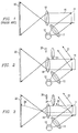
- FIG. 1 An optical block diagram for a typical reflective spatial light modulator display is shown in Figure 1.
- Light source 10 generates light which is transmitted via lens 12 to the x-y grid 14. The angles of reflection are discussed in further detail in Figures 4a-4c, but when the elements of the array are ON, they reflect the light down path 16 to the imaging lens 18. Imaging lens 18 then transmits the light, formed into an image at x-y grid 14, onto the screen 20.
- the OFF path is the same as the "flat" or unaddressed path.
- operation of the pointing device described herein requires that a method be provided to optically separate the image reflected from the screen from the image beam propagating to the screen.
- the separated, reflected screen image is then directed to the detector, which, together with associated hardware and software, locates the cursor image within the screen image and communicates that location to the CPU.
- the detector which, together with associated hardware and software, locates the cursor image within the screen image and communicates that location to the CPU.
- a different optical arrangement is necessary.
- the reflected screen image is mixed with light reflected in the "flat" direction, and a method of discriminating between the two signals must be provided. After this discrimination, the detector and its associated hardware and software must locate the cursor image within the screen image and communicate that location to the CPU as before.
- the light from the source 10 passes through lens 12 to the modulator array 14.
- the elements are OFF, as in Figure 2, the light does not travel path 16 from Figure 1, to the lens 18 and ultimately to the screen 20. Instead the light travels path 22.
- Lens 24 and detector 26 must lie away from the light coming from the OFF modulator elements so as to not produce a false pointing image. As can be seen in Figure 2, path 22 bypasses the lens 24 and therefore no light impinges detector 26.
- the light When the modulator is OFF, as in Figure 4c, the light reflects at a greater angle than when the modulator is merely flat, as was mentioned in Figures 2 and 3. However, when the modulator is OFF, as in Figure 4d, and light is being reimaged from the screen, this light travels the same path as the modulator's "flat" path.
- DMD digital micromirror device
- an active area mirror is suspended upon hinges between two posts.
- the mirror is addressed to one side or the other, causing the mirror to deflect to whichever side has the addressing signal.
- the DMD would torque to the left if the left side in Figure 4b had been addressed.
- the post and part of the hinges that are nearest the post do not twist to reflect the light as in Figures 4b or 4c. Therefore, some light will reflect as if the modulator were flat as in Figure 4a.
- DMDs can be manufactured to minimize the effect by concealing nonactive reflective surfaces, but diffraction from the mirror array will continue to direct light into the "flat" direction.
- This reflected light from the stationary element travels the same path as the light being reimaged by the screen. Somehow the light from the screen must be separated from the “flat” light. Encoding the light from the screen or using a specific frequency of light will eliminate this problem.
- the pointer could have both a visible source of light, for the user to see the pointer, and an invisible source of light, such as ultraviolet (UV) for the signal light.
- the detector could then have a filter in front of it that only allows UV light transmission.
- Another alternative is to coat the lens 24 with a coating that absorbs visible light. Either of these alternatives plus the many other ways the light could be separated will help reduce any "noise" light from the modulator 14 that could interfere with the detection.
- a second method to facilitate discrimination between the combination of light from the illumination beam and the reflected screen image and the pointing device illumination is to encode the pointing device illumination with a time modulated signal.
- analog and digital modulation is common use that would be appropriate, but most require a detector response time very short relative to the detector response time necessary to merely determine the location of the pointing cursor. Such fast detectors would lead to additional system cost, especially in systems using pixelated detectors to locate cursor position.
- CMOS complementary metal-oxide-semiconductor
- CCD charge-coupled device
- Hardware and software associated with the CCD must process the received image data to infer a location for the pointer.
- the detector would have to receive and process 307,200 pixels and send the location of the pointer to the CPU after it is located.
- Very few CCD or other pixelated arrays are fast enough to keep up with typical cursor motion and then have speed in reserve to decode a modulated signal.
- a better option might be a quadrant detector, which has the face of the detector divided into four quadrants, when the pointer is just located by the strength of signal falling into each quadrant, rather than by what exact pixel location at which the pointer is active.
- a detector can obviously be used for non-modulated signals as well.
- Another option is to have the signal light activated only when there is a task to be performed, similar to clicking a mouse on a task space in a personal computer. This could be achieved by adapting the detection part of the system as shown in Figure 5.
- the signal light would only be activated when a task must be performed, with a button similar to that on a hard-wired mouse.
- the pointing light is still usable for presentations, but the signal light is operated separately.
- a filter 40 such as those discussed previously and below, could separate a portion of the signal light from the other light, that separated light being directed to a smaller number of photodiodes 44 or some other type of fast photodetector through lens 42.
- the CPU 38 could receive a signal indicating that a task is to be performed only when the button is pushed. This would reduce processor load and perhaps eliminate the need for separate pointing device hardware. This process could be used to eliminate the need for visible illumination from the pointing device.
- the photodetector When the photodetector receives the signal, it could then insert the image of the pointer into the graphic being projected and thereby eliminate the need for the visible part of the pointer, except that needed to tell the operator where the pointer is. This would require constant position updates and consequently raise process load.
- IR sensors and detectors occur far more often than the similar components for W.
- IR light may not be practical. All of these light frequencies can be modulated using the AM, FM or digital pulse modulation techniques discussed above. The modulated light beams could then be separated using a filter passing only the particular modulation before the light from the screen impinges on the detector, thereby separating the desired signal from the noise.
- An advantage of this technique is that information concerning the manipulation of other cursor controls (of buttons) can be encoded into the modulation data stream.
- transmissive modulators similar concepts can be used, especially with transmissive modulators that require polarized coatings, such as liquid crystal displays (LCD).
- LCD liquid crystal displays
- a base system for such a modulator is shown in Figure 6.
- Light source 10 now resides on-axis with the screen 20.
- Light generated from source 10 travels through lens 12 and half-silvered mirror, or some similar component, 36, to modulator 14.
- the modulator in this case either transmits or blocks the light and sends the resultant image to the screen via lens 18.
- a pointer is used, all of the cells are addressed in the transmit mode.
- Other components instead of half-silvered mirrors could include cold or hot mirrors, or other optical components that reflect at some wavelengths and are transparent in the visible light realm.
- the projected dot from the pointer travels path 28 back through the lens 18 and through the all-transmitting modulator 14.
- the light impinges upon half-silvered mirror 36 which directs the light to lens 24 and detector 26.
- This type of system limits the amount of noise light.
- the half-silvered mirror could also reside in front of the modulator, as long as it passes light of the polarization that results from the modulator.
- the half-silvered mirror could instead be a polarizing filter, that allows light of a certain polarization through, after the light has been polarized by the LCD.
- Either system, for reflective or transmissive modulators allows the use of a pointer that is reimaged back from the screen onto a detector.
- the detector then converts the image of the pointer's cursor and sends the information to the CPU as an electronic signal which causes the CPU 38 to perform any tasks dictated by the signal.
- This system eliminates the need for a wired-in pointer, or an array of sensors that need to be positioned around the room. Such a system facilitates group interaction and ease of movement by having a portable pointer that is unrestricted.
Landscapes
- Engineering & Computer Science (AREA)
- General Engineering & Computer Science (AREA)
- Theoretical Computer Science (AREA)
- Physics & Mathematics (AREA)
- General Physics & Mathematics (AREA)
- Human Computer Interaction (AREA)
- Position Input By Displaying (AREA)
- User Interface Of Digital Computer (AREA)
- Devices For Indicating Variable Information By Combining Individual Elements (AREA)
Claims (11)
- Anzeigesystem mit:dadurch gekennzeichnet, daß das System ferner enthälteiner Lichtquelle (10);einem Bildschirm zur Wiedergabe eines Bildes;einem Zeiger zur Erzeugung eines Cursorbildes und zum Projizieren des Cursorbildes auf den Schirm (20); undeinem Detektor (26) zum Empfangen des Cursorbildes und zum Umsetzen des Cursorbildes in ein elektronisches Signal;eine digitale Mikrospiegelvorrichtung (14) mit einer Matrix aus ablenkbaren Spiegeln für den Empfang von Licht von der Lichtquelle (10), wobei jeder Spiegel der Matrix in eine Ein-Position und eine Aus-Position ablenkbar ist, sowie eine Projektionsoptik zum Projizieren eines Bildes auf den Schirm (20) durch Ablenken ausgewählter Spiegel der Matrix aus Spiegeln aus der Aus-Position in die Ein-Position zur Erzeugung eines Bildes auf dem Schirm (20); undeine Schaltungsanordnung (38) zum periodischen Einstellen aller Spiegel der Matrix aus Spiegeln in die Aus-Position und für den Empfang des elektronischen Signals, wenn sich alle Spiegel der Matrix aus Spiegeln in der Aus-Position befinden, um alle durch das Signal diktierten Aufgaben auszuführen; und daßdas Cursorbild auf den Schirm (20) so projiziert wird, daß das Cursorbild von dem Schirm (20) wieder auf die digitale Mikrospiegelvorrichtung (14) durch die Projektionsoptik abgebildet werden kann; und daß der Detektor das Cursorbild von der digitalen Mikrospiegelvorrichtung (14) empfängt, wenn die digitale Mikrospiegelvorrichtung (14) so adressiert worden ist, daß sich alle Spiegel der Matrix aus Spiegeln in der Aus-Position befinden.
- Anzeigesystem nach Anspruch 1, bei dem der Zeiger ein Bild des Cursors aus sichtbarem Licht mit einer gepulsten Frequenz des sichtbaren Lichts erzeugt.
- Anzeigesystem nach Anspruch 1 oder Anspruch 2, bei dem der Detektor (26) ferner ein Filter enthält.
- Anzeigesystem nach Anspruch 3, bei dem das Filter AM- FM- oder Impulsmodulation filtert.
- Anzeigesystem nach einem der Ansprüche 1 bis 4, bei dem der Detektor (26) eine CCD-Matrix enthält.
- Anzeigesystem nach einem der Ansprüche 1 bis 4, bei dem der Detektor (26) eine Fotodiode enthält.
- Anzeigesystem nach einem der Ansprüche 1 bis 6, bei dem der Zeiger ein Cursorbild im Ultraviolettbereich erzeugt.
- Anzeigesystem nach einem der Ansprüche 1 bis 6, bei dem der Zeiger ein Cursorbild im Infrarotbereich erzeugt.
- Anzeigesystem nach einem der Ansprüche 1 bis 8, bei dem der Zeiger zur Erzeugung eines Cursorbildes und zum Projizieren des Cursorbildes auf den Schirm (20) das Bild in zwei Komponenten teilen kann, eine erste sichtbare Komponente zur Betrachtung auf dem Schirm (20) und eine zweite Komponente einer spezifischen Lichtfrequenz für die Rückabbildung von dem Schirm (20).
- Anzeigesystem nach Anspruch 9, bei dem der Detektor (26) die zweite Komponente des Lichts empfangen und in ein elektrisches Signal umsetzen kann.
- Anzeigesystem nach Anspruch 9 oder Anspruch 10, bei dem die spezifische Frequenz des Lichts eine Impulsrate im sichtbaren Bereich aufweist.
Applications Claiming Priority (2)
| Application Number | Priority Date | Filing Date | Title |
|---|---|---|---|
| US24509394A | 1994-05-17 | 1994-05-17 | |
| US245093 | 1994-05-17 |
Publications (3)
| Publication Number | Publication Date |
|---|---|
| EP0686934A2 EP0686934A2 (de) | 1995-12-13 |
| EP0686934A3 EP0686934A3 (de) | 1996-08-21 |
| EP0686934B1 true EP0686934B1 (de) | 2001-09-26 |
Family
ID=22925250
Family Applications (1)
| Application Number | Title | Priority Date | Filing Date |
|---|---|---|---|
| EP95107225A Expired - Lifetime EP0686934B1 (de) | 1994-05-17 | 1995-05-12 | Anzeigevorrichtung mit Positionserkennung eines Zeigers |
Country Status (5)
| Country | Link |
|---|---|
| US (1) | US5654741A (de) |
| EP (1) | EP0686934B1 (de) |
| JP (1) | JPH08161114A (de) |
| KR (1) | KR950033432A (de) |
| DE (1) | DE69522856T2 (de) |
Cited By (1)
| Publication number | Priority date | Publication date | Assignee | Title |
|---|---|---|---|---|
| DE10208796A1 (de) * | 2002-03-01 | 2003-09-04 | Endress & Hauser Gmbh & Co Kg | Optoelektronisches Kommunikationssystem |
Families Citing this family (170)
| Publication number | Priority date | Publication date | Assignee | Title |
|---|---|---|---|---|
| US6674562B1 (en) | 1994-05-05 | 2004-01-06 | Iridigm Display Corporation | Interferometric modulation of radiation |
| US6467345B1 (en) | 1993-10-18 | 2002-10-22 | Xros, Inc. | Method of operating micromachined members coupled for relative rotation |
| US6044705A (en) * | 1993-10-18 | 2000-04-04 | Xros, Inc. | Micromachined members coupled for relative rotation by torsion bars |
| US7123216B1 (en) | 1994-05-05 | 2006-10-17 | Idc, Llc | Photonic MEMS and structures |
| US7138984B1 (en) | 2001-06-05 | 2006-11-21 | Idc, Llc | Directly laminated touch sensitive screen |
| US6680792B2 (en) | 1994-05-05 | 2004-01-20 | Iridigm Display Corporation | Interferometric modulation of radiation |
| US8014059B2 (en) | 1994-05-05 | 2011-09-06 | Qualcomm Mems Technologies, Inc. | System and method for charge control in a MEMS device |
| US7550794B2 (en) | 2002-09-20 | 2009-06-23 | Idc, Llc | Micromechanical systems device comprising a displaceable electrode and a charge-trapping layer |
| US7297471B1 (en) | 2003-04-15 | 2007-11-20 | Idc, Llc | Method for manufacturing an array of interferometric modulators |
| US7460291B2 (en) | 1994-05-05 | 2008-12-02 | Idc, Llc | Separable modulator |
| US7471444B2 (en) | 1996-12-19 | 2008-12-30 | Idc, Llc | Interferometric modulation of radiation |
| US5990992A (en) * | 1997-03-18 | 1999-11-23 | Nippon Sheet Glass Co., Ltd. | Image display device with plural planar microlens arrays |
| US5914783A (en) * | 1997-03-24 | 1999-06-22 | Mistubishi Electric Information Technology Center America, Inc. | Method and apparatus for detecting the location of a light source |
| KR100703140B1 (ko) | 1998-04-08 | 2007-04-05 | 이리다임 디스플레이 코포레이션 | 간섭 변조기 및 그 제조 방법 |
| US8928967B2 (en) | 1998-04-08 | 2015-01-06 | Qualcomm Mems Technologies, Inc. | Method and device for modulating light |
| US7532377B2 (en) | 1998-04-08 | 2009-05-12 | Idc, Llc | Movable micro-electromechanical device |
| US6219360B1 (en) | 1998-04-24 | 2001-04-17 | Trw Inc. | High average power solid-state laser system with phase front control |
| WO2003007049A1 (en) | 1999-10-05 | 2003-01-23 | Iridigm Display Corporation | Photonic mems and structures |
| JP4531272B2 (ja) * | 2001-01-16 | 2010-08-25 | 株式会社ワコム | 表示装置一体型位置検出装置 |
| US6589625B1 (en) | 2001-08-01 | 2003-07-08 | Iridigm Display Corporation | Hermetic seal and method to create the same |
| US6794119B2 (en) | 2002-02-12 | 2004-09-21 | Iridigm Display Corporation | Method for fabricating a structure for a microelectromechanical systems (MEMS) device |
| US6574033B1 (en) | 2002-02-27 | 2003-06-03 | Iridigm Display Corporation | Microelectromechanical systems device and method for fabricating same |
| US7781850B2 (en) | 2002-09-20 | 2010-08-24 | Qualcomm Mems Technologies, Inc. | Controlling electromechanical behavior of structures within a microelectromechanical systems device |
| TW200413810A (en) | 2003-01-29 | 2004-08-01 | Prime View Int Co Ltd | Light interference display panel and its manufacturing method |
| US20040169639A1 (en) * | 2003-02-28 | 2004-09-02 | Pate Michael A. | Visible pointer tracking with separately detectable pointer tracking signal |
| US7559656B2 (en) | 2003-03-03 | 2009-07-14 | Panasonic Corporation | Projector system |
| TW594360B (en) | 2003-04-21 | 2004-06-21 | Prime View Int Corp Ltd | A method for fabricating an interference display cell |
| TW570896B (en) | 2003-05-26 | 2004-01-11 | Prime View Int Co Ltd | A method for fabricating an interference display cell |
| US7221495B2 (en) | 2003-06-24 | 2007-05-22 | Idc Llc | Thin film precursor stack for MEMS manufacturing |
| TWI231865B (en) | 2003-08-26 | 2005-05-01 | Prime View Int Co Ltd | An interference display cell and fabrication method thereof |
| TW593126B (en) | 2003-09-30 | 2004-06-21 | Prime View Int Co Ltd | A structure of a micro electro mechanical system and manufacturing the same |
| US7012726B1 (en) | 2003-11-03 | 2006-03-14 | Idc, Llc | MEMS devices with unreleased thin film components |
| US7142346B2 (en) | 2003-12-09 | 2006-11-28 | Idc, Llc | System and method for addressing a MEMS display |
| US7161728B2 (en) | 2003-12-09 | 2007-01-09 | Idc, Llc | Area array modulation and lead reduction in interferometric modulators |
| US7532194B2 (en) | 2004-02-03 | 2009-05-12 | Idc, Llc | Driver voltage adjuster |
| US7119945B2 (en) | 2004-03-03 | 2006-10-10 | Idc, Llc | Altering temporal response of microelectromechanical elements |
| US7706050B2 (en) | 2004-03-05 | 2010-04-27 | Qualcomm Mems Technologies, Inc. | Integrated modulator illumination |
| US7720148B2 (en) * | 2004-03-26 | 2010-05-18 | The Hong Kong University Of Science And Technology | Efficient multi-frame motion estimation for video compression |
| US7476327B2 (en) | 2004-05-04 | 2009-01-13 | Idc, Llc | Method of manufacture for microelectromechanical devices |
| US7060895B2 (en) | 2004-05-04 | 2006-06-13 | Idc, Llc | Modifying the electro-mechanical behavior of devices |
| US7164520B2 (en) | 2004-05-12 | 2007-01-16 | Idc, Llc | Packaging for an interferometric modulator |
| WO2005119356A2 (en) * | 2004-05-28 | 2005-12-15 | Erik Jan Banning | Interactive direct-pointing system and calibration method |
| US7256922B2 (en) | 2004-07-02 | 2007-08-14 | Idc, Llc | Interferometric modulators with thin film transistors |
| KR101255691B1 (ko) | 2004-07-29 | 2013-04-17 | 퀄컴 엠이엠에스 테크놀로지스, 인크. | 간섭 변조기의 미소기전 동작을 위한 시스템 및 방법 |
| US7560299B2 (en) | 2004-08-27 | 2009-07-14 | Idc, Llc | Systems and methods of actuating MEMS display elements |
| US7515147B2 (en) | 2004-08-27 | 2009-04-07 | Idc, Llc | Staggered column drive circuit systems and methods |
| US7499208B2 (en) | 2004-08-27 | 2009-03-03 | Udc, Llc | Current mode display driver circuit realization feature |
| US7889163B2 (en) | 2004-08-27 | 2011-02-15 | Qualcomm Mems Technologies, Inc. | Drive method for MEMS devices |
| US7551159B2 (en) | 2004-08-27 | 2009-06-23 | Idc, Llc | System and method of sensing actuation and release voltages of an interferometric modulator |
| US7602375B2 (en) | 2004-09-27 | 2009-10-13 | Idc, Llc | Method and system for writing data to MEMS display elements |
| US7317568B2 (en) | 2004-09-27 | 2008-01-08 | Idc, Llc | System and method of implementation of interferometric modulators for display mirrors |
| US7527995B2 (en) | 2004-09-27 | 2009-05-05 | Qualcomm Mems Technologies, Inc. | Method of making prestructure for MEMS systems |
| US8008736B2 (en) | 2004-09-27 | 2011-08-30 | Qualcomm Mems Technologies, Inc. | Analog interferometric modulator device |
| US7424198B2 (en) | 2004-09-27 | 2008-09-09 | Idc, Llc | Method and device for packaging a substrate |
| US7813026B2 (en) | 2004-09-27 | 2010-10-12 | Qualcomm Mems Technologies, Inc. | System and method of reducing color shift in a display |
| US7920135B2 (en) | 2004-09-27 | 2011-04-05 | Qualcomm Mems Technologies, Inc. | Method and system for driving a bi-stable display |
| US8310441B2 (en) | 2004-09-27 | 2012-11-13 | Qualcomm Mems Technologies, Inc. | Method and system for writing data to MEMS display elements |
| US7583429B2 (en) | 2004-09-27 | 2009-09-01 | Idc, Llc | Ornamental display device |
| US7349136B2 (en) | 2004-09-27 | 2008-03-25 | Idc, Llc | Method and device for a display having transparent components integrated therein |
| US7310179B2 (en) | 2004-09-27 | 2007-12-18 | Idc, Llc | Method and device for selective adjustment of hysteresis window |
| US7259449B2 (en) | 2004-09-27 | 2007-08-21 | Idc, Llc | Method and system for sealing a substrate |
| US7343080B2 (en) | 2004-09-27 | 2008-03-11 | Idc, Llc | System and method of testing humidity in a sealed MEMS device |
| US7916103B2 (en) * | 2004-09-27 | 2011-03-29 | Qualcomm Mems Technologies, Inc. | System and method for display device with end-of-life phenomena |
| US7532195B2 (en) | 2004-09-27 | 2009-05-12 | Idc, Llc | Method and system for reducing power consumption in a display |
| US20060076634A1 (en) | 2004-09-27 | 2006-04-13 | Lauren Palmateer | Method and system for packaging MEMS devices with incorporated getter |
| US7535466B2 (en) | 2004-09-27 | 2009-05-19 | Idc, Llc | System with server based control of client device display features |
| US20060176487A1 (en) | 2004-09-27 | 2006-08-10 | William Cummings | Process control monitors for interferometric modulators |
| US7355780B2 (en) | 2004-09-27 | 2008-04-08 | Idc, Llc | System and method of illuminating interferometric modulators using backlighting |
| US7653371B2 (en) | 2004-09-27 | 2010-01-26 | Qualcomm Mems Technologies, Inc. | Selectable capacitance circuit |
| US8878825B2 (en) | 2004-09-27 | 2014-11-04 | Qualcomm Mems Technologies, Inc. | System and method for providing a variable refresh rate of an interferometric modulator display |
| US7299681B2 (en) | 2004-09-27 | 2007-11-27 | Idc, Llc | Method and system for detecting leak in electronic devices |
| US7136213B2 (en) | 2004-09-27 | 2006-11-14 | Idc, Llc | Interferometric modulators having charge persistence |
| US7692839B2 (en) | 2004-09-27 | 2010-04-06 | Qualcomm Mems Technologies, Inc. | System and method of providing MEMS device with anti-stiction coating |
| US7936497B2 (en) | 2004-09-27 | 2011-05-03 | Qualcomm Mems Technologies, Inc. | MEMS device having deformable membrane characterized by mechanical persistence |
| US7289259B2 (en) | 2004-09-27 | 2007-10-30 | Idc, Llc | Conductive bus structure for interferometric modulator array |
| US7373026B2 (en) | 2004-09-27 | 2008-05-13 | Idc, Llc | MEMS device fabricated on a pre-patterned substrate |
| US7710629B2 (en) | 2004-09-27 | 2010-05-04 | Qualcomm Mems Technologies, Inc. | System and method for display device with reinforcing substance |
| US7564612B2 (en) | 2004-09-27 | 2009-07-21 | Idc, Llc | Photonic MEMS and structures |
| US7586484B2 (en) | 2004-09-27 | 2009-09-08 | Idc, Llc | Controller and driver features for bi-stable display |
| US7453579B2 (en) | 2004-09-27 | 2008-11-18 | Idc, Llc | Measurement of the dynamic characteristics of interferometric modulators |
| US7684104B2 (en) | 2004-09-27 | 2010-03-23 | Idc, Llc | MEMS using filler material and method |
| US7372613B2 (en) | 2004-09-27 | 2008-05-13 | Idc, Llc | Method and device for multistate interferometric light modulation |
| US7289256B2 (en) | 2004-09-27 | 2007-10-30 | Idc, Llc | Electrical characterization of interferometric modulators |
| US7417783B2 (en) | 2004-09-27 | 2008-08-26 | Idc, Llc | Mirror and mirror layer for optical modulator and method |
| US7369296B2 (en) | 2004-09-27 | 2008-05-06 | Idc, Llc | Device and method for modifying actuation voltage thresholds of a deformable membrane in an interferometric modulator |
| US7446927B2 (en) | 2004-09-27 | 2008-11-04 | Idc, Llc | MEMS switch with set and latch electrodes |
| US7492502B2 (en) | 2004-09-27 | 2009-02-17 | Idc, Llc | Method of fabricating a free-standing microstructure |
| US7415186B2 (en) | 2004-09-27 | 2008-08-19 | Idc, Llc | Methods for visually inspecting interferometric modulators for defects |
| US7345805B2 (en) | 2004-09-27 | 2008-03-18 | Idc, Llc | Interferometric modulator array with integrated MEMS electrical switches |
| US7724993B2 (en) | 2004-09-27 | 2010-05-25 | Qualcomm Mems Technologies, Inc. | MEMS switches with deforming membranes |
| BRPI0509575A (pt) | 2004-09-27 | 2007-10-09 | Idc Llc | método e dispositivo para modulação de luz interferométrica de multi-estados |
| US7668415B2 (en) | 2004-09-27 | 2010-02-23 | Qualcomm Mems Technologies, Inc. | Method and device for providing electronic circuitry on a backplate |
| US7626581B2 (en) | 2004-09-27 | 2009-12-01 | Idc, Llc | Device and method for display memory using manipulation of mechanical response |
| US7417735B2 (en) | 2004-09-27 | 2008-08-26 | Idc, Llc | Systems and methods for measuring color and contrast in specular reflective devices |
| US7808703B2 (en) | 2004-09-27 | 2010-10-05 | Qualcomm Mems Technologies, Inc. | System and method for implementation of interferometric modulator displays |
| US7304784B2 (en) | 2004-09-27 | 2007-12-04 | Idc, Llc | Reflective display device having viewable display on both sides |
| US7553684B2 (en) | 2004-09-27 | 2009-06-30 | Idc, Llc | Method of fabricating interferometric devices using lift-off processing techniques |
| US7630119B2 (en) | 2004-09-27 | 2009-12-08 | Qualcomm Mems Technologies, Inc. | Apparatus and method for reducing slippage between structures in an interferometric modulator |
| US7420725B2 (en) | 2004-09-27 | 2008-09-02 | Idc, Llc | Device having a conductive light absorbing mask and method for fabricating same |
| US8124434B2 (en) | 2004-09-27 | 2012-02-28 | Qualcomm Mems Technologies, Inc. | Method and system for packaging a display |
| US7843410B2 (en) | 2004-09-27 | 2010-11-30 | Qualcomm Mems Technologies, Inc. | Method and device for electrically programmable display |
| US7460246B2 (en) | 2004-09-27 | 2008-12-02 | Idc, Llc | Method and system for sensing light using interferometric elements |
| US7545550B2 (en) | 2004-09-27 | 2009-06-09 | Idc, Llc | Systems and methods of actuating MEMS display elements |
| US7405924B2 (en) | 2004-09-27 | 2008-07-29 | Idc, Llc | System and method for protecting microelectromechanical systems array using structurally reinforced back-plate |
| US7675669B2 (en) | 2004-09-27 | 2010-03-09 | Qualcomm Mems Technologies, Inc. | Method and system for driving interferometric modulators |
| US7893919B2 (en) | 2004-09-27 | 2011-02-22 | Qualcomm Mems Technologies, Inc. | Display region architectures |
| US7719500B2 (en) | 2004-09-27 | 2010-05-18 | Qualcomm Mems Technologies, Inc. | Reflective display pixels arranged in non-rectangular arrays |
| US7405861B2 (en) | 2004-09-27 | 2008-07-29 | Idc, Llc | Method and device for protecting interferometric modulators from electrostatic discharge |
| US7130104B2 (en) | 2004-09-27 | 2006-10-31 | Idc, Llc | Methods and devices for inhibiting tilting of a mirror in an interferometric modulator |
| US7679627B2 (en) | 2004-09-27 | 2010-03-16 | Qualcomm Mems Technologies, Inc. | Controller and driver features for bi-stable display |
| US7368803B2 (en) | 2004-09-27 | 2008-05-06 | Idc, Llc | System and method for protecting microelectromechanical systems array using back-plate with non-flat portion |
| US7359066B2 (en) | 2004-09-27 | 2008-04-15 | Idc, Llc | Electro-optical measurement of hysteresis in interferometric modulators |
| US7420728B2 (en) | 2004-09-27 | 2008-09-02 | Idc, Llc | Methods of fabricating interferometric modulators by selectively removing a material |
| US7161730B2 (en) | 2004-09-27 | 2007-01-09 | Idc, Llc | System and method for providing thermal compensation for an interferometric modulator display |
| US7554714B2 (en) | 2004-09-27 | 2009-06-30 | Idc, Llc | Device and method for manipulation of thermal response in a modulator |
| US7327510B2 (en) | 2004-09-27 | 2008-02-05 | Idc, Llc | Process for modifying offset voltage characteristics of an interferometric modulator |
| US7369294B2 (en) | 2004-09-27 | 2008-05-06 | Idc, Llc | Ornamental display device |
| US7944599B2 (en) | 2004-09-27 | 2011-05-17 | Qualcomm Mems Technologies, Inc. | Electromechanical device with optical function separated from mechanical and electrical function |
| US7302157B2 (en) | 2004-09-27 | 2007-11-27 | Idc, Llc | System and method for multi-level brightness in interferometric modulation |
| US7701631B2 (en) | 2004-09-27 | 2010-04-20 | Qualcomm Mems Technologies, Inc. | Device having patterned spacers for backplates and method of making the same |
| US7321456B2 (en) | 2004-09-27 | 2008-01-22 | Idc, Llc | Method and device for corner interferometric modulation |
| US7405389B2 (en) * | 2004-11-19 | 2008-07-29 | Silicon Light Machines Corporation | Dense multi-axis array for motion sensing |
| TW200628877A (en) | 2005-02-04 | 2006-08-16 | Prime View Int Co Ltd | Method of manufacturing optical interference type color display |
| US7920136B2 (en) | 2005-05-05 | 2011-04-05 | Qualcomm Mems Technologies, Inc. | System and method of driving a MEMS display device |
| CA2607807A1 (en) | 2005-05-05 | 2006-11-16 | Qualcomm Incorporated | Dynamic driver ic and display panel configuration |
| US7948457B2 (en) | 2005-05-05 | 2011-05-24 | Qualcomm Mems Technologies, Inc. | Systems and methods of actuating MEMS display elements |
| US20060284832A1 (en) * | 2005-06-16 | 2006-12-21 | H.P.B. Optoelectronics Co., Ltd. | Method and apparatus for locating a laser spot |
| US9285897B2 (en) | 2005-07-13 | 2016-03-15 | Ultimate Pointer, L.L.C. | Easily deployable interactive direct-pointing system and calibration method therefor |
| JP2009503564A (ja) | 2005-07-22 | 2009-01-29 | クアルコム,インコーポレイテッド | Memsデバイスのための支持構造、およびその方法 |
| US7355779B2 (en) | 2005-09-02 | 2008-04-08 | Idc, Llc | Method and system for driving MEMS display elements |
| US7630114B2 (en) | 2005-10-28 | 2009-12-08 | Idc, Llc | Diffusion barrier layer for MEMS devices |
| US8391630B2 (en) | 2005-12-22 | 2013-03-05 | Qualcomm Mems Technologies, Inc. | System and method for power reduction when decompressing video streams for interferometric modulator displays |
| US7795061B2 (en) | 2005-12-29 | 2010-09-14 | Qualcomm Mems Technologies, Inc. | Method of creating MEMS device cavities by a non-etching process |
| US7636151B2 (en) | 2006-01-06 | 2009-12-22 | Qualcomm Mems Technologies, Inc. | System and method for providing residual stress test structures |
| US7916980B2 (en) | 2006-01-13 | 2011-03-29 | Qualcomm Mems Technologies, Inc. | Interconnect structure for MEMS device |
| US7382515B2 (en) | 2006-01-18 | 2008-06-03 | Qualcomm Mems Technologies, Inc. | Silicon-rich silicon nitrides as etch stops in MEMS manufacture |
| US8194056B2 (en) | 2006-02-09 | 2012-06-05 | Qualcomm Mems Technologies Inc. | Method and system for writing data to MEMS display elements |
| US7582952B2 (en) | 2006-02-21 | 2009-09-01 | Qualcomm Mems Technologies, Inc. | Method for providing and removing discharging interconnect for chip-on-glass output leads and structures thereof |
| US7547568B2 (en) | 2006-02-22 | 2009-06-16 | Qualcomm Mems Technologies, Inc. | Electrical conditioning of MEMS device and insulating layer thereof |
| US7550810B2 (en) | 2006-02-23 | 2009-06-23 | Qualcomm Mems Technologies, Inc. | MEMS device having a layer movable at asymmetric rates |
| US7450295B2 (en) | 2006-03-02 | 2008-11-11 | Qualcomm Mems Technologies, Inc. | Methods for producing MEMS with protective coatings using multi-component sacrificial layers |
| US7643203B2 (en) | 2006-04-10 | 2010-01-05 | Qualcomm Mems Technologies, Inc. | Interferometric optical display system with broadband characteristics |
| US7903047B2 (en) | 2006-04-17 | 2011-03-08 | Qualcomm Mems Technologies, Inc. | Mode indicator for interferometric modulator displays |
| US7711239B2 (en) | 2006-04-19 | 2010-05-04 | Qualcomm Mems Technologies, Inc. | Microelectromechanical device and method utilizing nanoparticles |
| US7623287B2 (en) | 2006-04-19 | 2009-11-24 | Qualcomm Mems Technologies, Inc. | Non-planar surface structures and process for microelectromechanical systems |
| US7527996B2 (en) | 2006-04-19 | 2009-05-05 | Qualcomm Mems Technologies, Inc. | Non-planar surface structures and process for microelectromechanical systems |
| US7417784B2 (en) | 2006-04-19 | 2008-08-26 | Qualcomm Mems Technologies, Inc. | Microelectromechanical device and method utilizing a porous surface |
| US8049713B2 (en) | 2006-04-24 | 2011-11-01 | Qualcomm Mems Technologies, Inc. | Power consumption optimized display update |
| US7369292B2 (en) | 2006-05-03 | 2008-05-06 | Qualcomm Mems Technologies, Inc. | Electrode and interconnect materials for MEMS devices |
| US7321457B2 (en) | 2006-06-01 | 2008-01-22 | Qualcomm Incorporated | Process and structure for fabrication of MEMS device having isolated edge posts |
| US7405863B2 (en) | 2006-06-01 | 2008-07-29 | Qualcomm Mems Technologies, Inc. | Patterning of mechanical layer in MEMS to reduce stresses at supports |
| US7649671B2 (en) | 2006-06-01 | 2010-01-19 | Qualcomm Mems Technologies, Inc. | Analog interferometric modulator device with electrostatic actuation and release |
| US7471442B2 (en) | 2006-06-15 | 2008-12-30 | Qualcomm Mems Technologies, Inc. | Method and apparatus for low range bit depth enhancements for MEMS display architectures |
| US7702192B2 (en) | 2006-06-21 | 2010-04-20 | Qualcomm Mems Technologies, Inc. | Systems and methods for driving MEMS display |
| US7835061B2 (en) | 2006-06-28 | 2010-11-16 | Qualcomm Mems Technologies, Inc. | Support structures for free-standing electromechanical devices |
| US7385744B2 (en) | 2006-06-28 | 2008-06-10 | Qualcomm Mems Technologies, Inc. | Support structure for free-standing MEMS device and methods for forming the same |
| US7777715B2 (en) | 2006-06-29 | 2010-08-17 | Qualcomm Mems Technologies, Inc. | Passive circuits for de-multiplexing display inputs |
| US7527998B2 (en) | 2006-06-30 | 2009-05-05 | Qualcomm Mems Technologies, Inc. | Method of manufacturing MEMS devices providing air gap control |
| US7388704B2 (en) | 2006-06-30 | 2008-06-17 | Qualcomm Mems Technologies, Inc. | Determination of interferometric modulator mirror curvature and airgap variation using digital photographs |
| US7763546B2 (en) | 2006-08-02 | 2010-07-27 | Qualcomm Mems Technologies, Inc. | Methods for reducing surface charges during the manufacture of microelectromechanical systems devices |
| US7566664B2 (en) | 2006-08-02 | 2009-07-28 | Qualcomm Mems Technologies, Inc. | Selective etching of MEMS using gaseous halides and reactive co-etchants |
| US8089455B1 (en) | 2006-11-28 | 2012-01-03 | Wieder James W | Remote control with a single control button |
| US7719752B2 (en) | 2007-05-11 | 2010-05-18 | Qualcomm Mems Technologies, Inc. | MEMS structures, methods of fabricating MEMS components on separate substrates and assembly of same |
| US20090160768A1 (en) * | 2007-12-21 | 2009-06-25 | Nvidia Corporation | Enhanced Presentation Capabilities Using a Pointer Implement |
| US8736590B2 (en) | 2009-03-27 | 2014-05-27 | Qualcomm Mems Technologies, Inc. | Low voltage driver scheme for interferometric modulators |
| US9071834B2 (en) * | 2009-04-25 | 2015-06-30 | James Yett | Array of individually angled mirrors reflecting disparate color sources toward one or more viewing positions to construct images and visual effects |
| EP2556403A1 (de) | 2010-04-09 | 2013-02-13 | Qualcomm Mems Technologies, Inc. | Mechanische schicht einer elektromechanischen vorrichtung und verfahren zu ihrer herstellung |
| US9134527B2 (en) | 2011-04-04 | 2015-09-15 | Qualcomm Mems Technologies, Inc. | Pixel via and methods of forming the same |
| US8963159B2 (en) | 2011-04-04 | 2015-02-24 | Qualcomm Mems Technologies, Inc. | Pixel via and methods of forming the same |
| JP2015158644A (ja) * | 2014-02-25 | 2015-09-03 | カシオ計算機株式会社 | 投影装置、投影方法及びプログラム |
Family Cites Families (7)
| Publication number | Priority date | Publication date | Assignee | Title |
|---|---|---|---|---|
| US4280135A (en) * | 1979-06-01 | 1981-07-21 | Schlossberg Howard R | Remote pointing system |
| US4832447A (en) * | 1987-12-04 | 1989-05-23 | Board Of Trustees Operating Michigan State University | Joint transform image correlation using a nonlinear spatial light modulator at the fourier plane |
| US5181015A (en) * | 1989-11-07 | 1993-01-19 | Proxima Corporation | Method and apparatus for calibrating an optical computer input system |
| JP2681304B2 (ja) * | 1990-05-16 | 1997-11-26 | 日本ビクター株式会社 | 表示装置 |
| DE4129602A1 (de) * | 1990-09-15 | 1992-03-19 | Fraunhofer Ges Forschung | Vorrichtung zur dateneingabe |
| CA2051204C (en) * | 1990-11-02 | 1999-04-20 | Scott A. Elrod | Position and function input system for a large area display |
| JPH04263236A (ja) * | 1991-02-19 | 1992-09-18 | Nec Corp | 投射型液晶表示装置 |
-
1995
- 1995-05-12 DE DE69522856T patent/DE69522856T2/de not_active Expired - Fee Related
- 1995-05-12 KR KR1019950011682A patent/KR950033432A/ko not_active Withdrawn
- 1995-05-12 EP EP95107225A patent/EP0686934B1/de not_active Expired - Lifetime
- 1995-05-17 JP JP11866595A patent/JPH08161114A/ja active Pending
- 1995-12-05 US US08/567,439 patent/US5654741A/en not_active Expired - Lifetime
Cited By (1)
| Publication number | Priority date | Publication date | Assignee | Title |
|---|---|---|---|---|
| DE10208796A1 (de) * | 2002-03-01 | 2003-09-04 | Endress & Hauser Gmbh & Co Kg | Optoelektronisches Kommunikationssystem |
Also Published As
| Publication number | Publication date |
|---|---|
| US5654741A (en) | 1997-08-05 |
| EP0686934A3 (de) | 1996-08-21 |
| DE69522856T2 (de) | 2002-05-02 |
| KR950033432A (ko) | 1995-12-26 |
| JPH08161114A (ja) | 1996-06-21 |
| DE69522856D1 (de) | 2001-10-31 |
| EP0686934A2 (de) | 1995-12-13 |
Similar Documents
| Publication | Publication Date | Title |
|---|---|---|
| EP0686934B1 (de) | Anzeigevorrichtung mit Positionserkennung eines Zeigers | |
| US6707444B1 (en) | Projector and camera arrangement with shared optics and optical marker for use with whiteboard systems | |
| US8284173B2 (en) | System and method of detecting contact on a display | |
| US7025461B2 (en) | Interactive display system having a digital micromirror imaging device | |
| JP2648553B2 (ja) | 入力デバイス | |
| US5973672A (en) | Multiple participant interactive interface | |
| EP0137845A1 (de) | Doppelbildfeld-sensor. | |
| JPH0253131A (ja) | グラフィックタブレット付きディスプレイ | |
| US8690340B2 (en) | Combined image projection and capture system using on and off state positions of spatial light modulator | |
| WO2022158209A1 (ja) | 空間浮遊映像表示装置 | |
| JP7701540B2 (ja) | 空間浮遊映像表示装置 | |
| WO2008156453A1 (en) | Laser pointer for an interactive display | |
| WO1996029677A1 (en) | An interactive display and input device | |
| WO2003063069A2 (en) | Touch screen | |
| US7167619B2 (en) | Interactive display system having a matrix optical detector | |
| EP1660921A2 (de) | Interaktives display-system mit einer skalierten virtuellen zielzone | |
| JP3184898B2 (ja) | 画像表示装置の表示位置指示方式 | |
| JPH07261911A (ja) | 光ファイバ式タッチパネル | |
| JPS61202218A (ja) | 入出力装置 | |
| WO2008156457A1 (en) | Interactive display with camera feedback |
Legal Events
| Date | Code | Title | Description |
|---|---|---|---|
| PUAI | Public reference made under article 153(3) epc to a published international application that has entered the european phase |
Free format text: ORIGINAL CODE: 0009012 |
|
| AK | Designated contracting states |
Kind code of ref document: A2 Designated state(s): DE FR GB IT NL |
|
| PUAL | Search report despatched |
Free format text: ORIGINAL CODE: 0009013 |
|
| AK | Designated contracting states |
Kind code of ref document: A3 Designated state(s): DE FR GB IT NL |
|
| 17P | Request for examination filed |
Effective date: 19970205 |
|
| 17Q | First examination report despatched |
Effective date: 19990525 |
|
| GRAG | Despatch of communication of intention to grant |
Free format text: ORIGINAL CODE: EPIDOS AGRA |
|
| GRAG | Despatch of communication of intention to grant |
Free format text: ORIGINAL CODE: EPIDOS AGRA |
|
| GRAH | Despatch of communication of intention to grant a patent |
Free format text: ORIGINAL CODE: EPIDOS IGRA |
|
| GRAH | Despatch of communication of intention to grant a patent |
Free format text: ORIGINAL CODE: EPIDOS IGRA |
|
| GRAA | (expected) grant |
Free format text: ORIGINAL CODE: 0009210 |
|
| AK | Designated contracting states |
Kind code of ref document: B1 Designated state(s): DE FR GB IT NL |
|
| REF | Corresponds to: |
Ref document number: 69522856 Country of ref document: DE Date of ref document: 20011031 |
|
| ET | Fr: translation filed | ||
| REG | Reference to a national code |
Ref country code: GB Ref legal event code: IF02 |
|
| PGFP | Annual fee paid to national office [announced via postgrant information from national office to epo] |
Ref country code: NL Payment date: 20020325 Year of fee payment: 8 |
|
| PGFP | Annual fee paid to national office [announced via postgrant information from national office to epo] |
Ref country code: GB Payment date: 20020404 Year of fee payment: 8 |
|
| PGFP | Annual fee paid to national office [announced via postgrant information from national office to epo] |
Ref country code: FR Payment date: 20020503 Year of fee payment: 8 |
|
| PGFP | Annual fee paid to national office [announced via postgrant information from national office to epo] |
Ref country code: DE Payment date: 20020531 Year of fee payment: 8 |
|
| PLBE | No opposition filed within time limit |
Free format text: ORIGINAL CODE: 0009261 |
|
| STAA | Information on the status of an ep patent application or granted ep patent |
Free format text: STATUS: NO OPPOSITION FILED WITHIN TIME LIMIT |
|
| 26N | No opposition filed | ||
| PG25 | Lapsed in a contracting state [announced via postgrant information from national office to epo] |
Ref country code: GB Free format text: LAPSE BECAUSE OF NON-PAYMENT OF DUE FEES Effective date: 20030512 |
|
| PG25 | Lapsed in a contracting state [announced via postgrant information from national office to epo] |
Ref country code: NL Free format text: LAPSE BECAUSE OF NON-PAYMENT OF DUE FEES Effective date: 20031201 |
|
| PG25 | Lapsed in a contracting state [announced via postgrant information from national office to epo] |
Ref country code: DE Free format text: LAPSE BECAUSE OF NON-PAYMENT OF DUE FEES Effective date: 20031202 |
|
| GBPC | Gb: european patent ceased through non-payment of renewal fee |
Effective date: 20030512 |
|
| PG25 | Lapsed in a contracting state [announced via postgrant information from national office to epo] |
Ref country code: FR Free format text: LAPSE BECAUSE OF NON-PAYMENT OF DUE FEES Effective date: 20040130 |
|
| NLV4 | Nl: lapsed or anulled due to non-payment of the annual fee |
Effective date: 20031201 |
|
| REG | Reference to a national code |
Ref country code: FR Ref legal event code: ST |
|
| PG25 | Lapsed in a contracting state [announced via postgrant information from national office to epo] |
Ref country code: IT Free format text: LAPSE BECAUSE OF NON-PAYMENT OF DUE FEES;WARNING: LAPSES OF ITALIAN PATENTS WITH EFFECTIVE DATE BEFORE 2007 MAY HAVE OCCURRED AT ANY TIME BEFORE 2007. THE CORRECT EFFECTIVE DATE MAY BE DIFFERENT FROM THE ONE RECORDED. Effective date: 20050512 |