EP0686975A1 - Ausgangsdatenpufferschaltung für integrierte Halbleiterschaltung - Google Patents
Ausgangsdatenpufferschaltung für integrierte Halbleiterschaltung Download PDFInfo
- Publication number
- EP0686975A1 EP0686975A1 EP95113987A EP95113987A EP0686975A1 EP 0686975 A1 EP0686975 A1 EP 0686975A1 EP 95113987 A EP95113987 A EP 95113987A EP 95113987 A EP95113987 A EP 95113987A EP 0686975 A1 EP0686975 A1 EP 0686975A1
- Authority
- EP
- European Patent Office
- Prior art keywords
- circuit
- output buffer
- output
- delay
- transistors
- Prior art date
- Legal status (The legal status is an assumption and is not a legal conclusion. Google has not performed a legal analysis and makes no representation as to the accuracy of the status listed.)
- Withdrawn
Links
- 239000000872 buffer Substances 0.000 title claims abstract description 52
- 239000004065 semiconductor Substances 0.000 title claims abstract description 7
- 230000003111 delayed effect Effects 0.000 claims description 3
- 238000010586 diagram Methods 0.000 description 14
- 230000008859 change Effects 0.000 description 5
- 230000007257 malfunction Effects 0.000 description 5
- 238000000034 method Methods 0.000 description 3
- 239000003990 capacitor Substances 0.000 description 2
- 230000008569 process Effects 0.000 description 2
- 230000004044 response Effects 0.000 description 2
- 230000000717 retained effect Effects 0.000 description 2
- 230000002159 abnormal effect Effects 0.000 description 1
- 230000000903 blocking effect Effects 0.000 description 1
- 230000000694 effects Effects 0.000 description 1
- 230000006870 function Effects 0.000 description 1
- 230000002093 peripheral effect Effects 0.000 description 1
- 230000009467 reduction Effects 0.000 description 1
- 230000000630 rising effect Effects 0.000 description 1
- 230000001052 transient effect Effects 0.000 description 1
Images


Classifications
-
- H—ELECTRICITY
- H03—ELECTRONIC CIRCUITRY
- H03K—PULSE TECHNIQUE
- H03K19/00—Logic circuits, i.e. having at least two inputs acting on one output; Inverting circuits
- H03K19/02—Logic circuits, i.e. having at least two inputs acting on one output; Inverting circuits using specified components
- H03K19/08—Logic circuits, i.e. having at least two inputs acting on one output; Inverting circuits using specified components using semiconductor devices
- H03K19/094—Logic circuits, i.e. having at least two inputs acting on one output; Inverting circuits using specified components using semiconductor devices using field-effect transistors
- H03K19/0944—Logic circuits, i.e. having at least two inputs acting on one output; Inverting circuits using specified components using semiconductor devices using field-effect transistors using MOSFET or insulated gate field-effect transistors, i.e. IGFET
- H03K19/0948—Logic circuits, i.e. having at least two inputs acting on one output; Inverting circuits using specified components using semiconductor devices using field-effect transistors using MOSFET or insulated gate field-effect transistors, i.e. IGFET using CMOS or complementary insulated gate field-effect transistors
-
- G—PHYSICS
- G11—INFORMATION STORAGE
- G11C—STATIC STORES
- G11C7/00—Arrangements for writing information into, or reading information out from, a digital store
- G11C7/10—Input/output [I/O] data interface arrangements, e.g. I/O data control circuits, I/O data buffers
- G11C7/1051—Data output circuits, e.g. read-out amplifiers, data output buffers, data output registers, data output level conversion circuits
- G11C7/1057—Data output buffers, e.g. comprising level conversion circuits, circuits for adapting load
-
- G—PHYSICS
- G11—INFORMATION STORAGE
- G11C—STATIC STORES
- G11C7/00—Arrangements for writing information into, or reading information out from, a digital store
- G11C7/10—Input/output [I/O] data interface arrangements, e.g. I/O data control circuits, I/O data buffers
- G11C7/1051—Data output circuits, e.g. read-out amplifiers, data output buffers, data output registers, data output level conversion circuits
-
- G—PHYSICS
- G11—INFORMATION STORAGE
- G11C—STATIC STORES
- G11C2207/00—Indexing scheme relating to arrangements for writing information into, or reading information out from, a digital store
- G11C2207/10—Aspects relating to interfaces of memory device to external buses
- G11C2207/108—Wide data ports
Definitions
- the present invention relates to a data output buffer circuit for a semiconductor integrated circuit.
- a microprocessor, its peripheral LSI, and the like have a number of output buffers OB for outputting an address signal and a data signal.
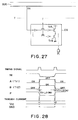
- a 16 bit microprocessor has, for example, 20 output buffers for outputting an address/data signal. Examples of the internal circuit of each output buffer OB are shown in Figs. 26 and 27.
- Each output buffer OB is controlled by a timing signal T to output an address/data signal supplied from a bus BUS such as an address bus and data bus.
- a bus BUS such as an address bus and data bus.
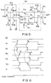
- Fig. 28 shows a through current flowing in the output buffer OB shown in Fig. 26 when an output signal is inverted. As seen from Fig. 26, a through current will flow at time tl and time t2 when an output of the output buffer is inverted from "1" to "O" and from "0" to "1", respectively.
- the output buffers OB are all controlled by the same timing signal T, so that a through current may flow through a plurality of output buffers OB at the same time.
- the total through current may take a value in the order of ampere.
- a number of output buffers OB shown in Fig. 25 operate in response to the same timing signal as described above. Therefore, for example, if many of output buffers change its output level from “H” level to “L” level, a rush current flowing through the ground pin (GND) of the semiconductor integrated circuit takes a value in the order of ampere. Thus, the potential (internal power source potential) at the ground pin rises, resulting in a malfunction.
- Fig. 29 illustrates a rise of the ground (GND) potential when all output buffers OB change its output level from "1" level to "O" level.
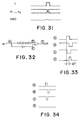
- the timing signal is supplied via delay means DL to each output buffer OB in order to prevent the ground potential from rising, as seen from Fig. 30. Therefore, as shown in Fig. 31, the operation timings of the output buffers OB are shifted sequentially so that the total current flowing at any timing can be suppressed to a small value.
- the pulse width of the timing signal T is generally the same as that of the main clock used within the LSI, so that sometimes an output pulse may not be obtained from the timing signal after it has passed through the delay means.
- Fig. 32 shows an example of a delay means
- Fig. 33 illustrate a normal state where a pulse is outputted
- Fig. 34 illustrates an abnormal state where a pulse is not outputted. If a pulse indicated at "A" in Fig. 33 is applied to the input IN of the delay means shown in Fig. 32, there are obtained pulses indicated at "B” and "C” in Fig. 33 at the circuit portions shown in Fig.
- a delay time is represented by DT. If the input pulse width is narrowed so as to speed up the operation time as seen from Fig. 34, there is obtained no pulse as indicated at "D” in Fig. 34. In other words, if delay means are used, it is not possible to make high the operation frequency (speed) of a semiconductor integrated circuit.
- the present invention has been made in consideration of the above circumstances, and aims at providing a semiconductor integrated circuit capable of effectively suppressing power source noises. This object is achieved by a circuit having the features listed in claim 1. Advantageous embodiments are contained in the subclaims.
- a noise eliminator circuit or a delay circuit for delaying either a leading edge or a trailing edge can be realized with a smaller number of transistors than conventional.
- Figs. 1 to 8 are circuit diagrams and operation timing charts of the first to fourth embodiments wherein a through current is prevented from flowing into an output buffer OB at the time of changing an output level thereof.
- two output transistors Trl and Tr2 (P- and N-type transistors) at the output terminal are turned off (with the output levels being high impedance Z) prior to the level change of an output signal, and in this state one of the transistors Trl and Tr2 is turned on and the other is turned off, to thereby establish the output level while blocking a through current.
- an input data such as an address signal and a data signal from a memory cell, a register and the like is applied to an input terminal IN connected to an inverter IV1.
- An output terminal of the inverter IV1 is connected to the gate of an output transistor Trl via a transistor Trll, and to the gate of an output transistor Tr2 via a transistor Trl2.
- the transistors Trll and Trl2 are connected in parallel with transistors Trl3 and Trl4.
- the gates of the transistors Trl and Tr2 are pulled up and down by transistors Trl5 and Trl6, respectively.
- the output terminal of the inverter IV1 is also connected to a delay circuit DL1.
- the output terminal of the delay circuit DL1 is connected to the gates of the transistors Trll and Trl2, and to an inverter IV2 whose output terminal is connected to the gate of the transistors Trl3 to Trl6.
- the circuit shown in Fig. 1 operates as follows. Referring to Fig. 2, when the signal at the input terminal IN falls at time tl, the level at point Al rises because of the function of the inverter IV1. This level rise is transmitted via the transistor Trll to point Cl to raise the level at point Cl. This level rise at point Cl causes the output transistor (P-type) Trl to turn off. At this time, the level at point Dl is "L" level so that the transistor Tr2 also is caused to turn off. As a result, the output level of the transistors Trl and Tr2 enters a high impedance state after time tl. The level rise at point Al is transmitted to and reaches point Bl via the delay circuit DL1 at time t2.
- the level at point Dl rises so that the transistor Tr2 turns on and the level at the output terminal P lowers to "L" .
- the above operation can be understood from curved arrows indicated near at times tl and t2 in Fig. 2.
- the transistor Tr2 is turned on during the delay time F of the delay circuit DL1, i.e., during the off-state or high impedance state of both the transistors Trl and Tr2. A through current will not flow accordingly through the transistors Trl and Tr2, thereby suppressing the potential change of the power source line.
- Transistors Tr21 to Tr23 as well as transistors Tr24 to Tr26 are serially connected between a pair of power sources V CC and V SS .
- An input terminal IN is connected to the gates of the transistors Tr21 and Tr22, and to the gates of the transistors Tr25 and Tr26.
- the input terminal IN is also connected via a delay circuit DL2 to the gates of the transistors Tr23 and Tr24.
- the interconnection between the transistors Tr21 and Tr22 is connected to the gate of a transistor Trl.
- the interconnection between the transistors Tr25 and Tr26 is connected to the gate of a transistor Tr2.
- the circuit shown in Fig. 3 operates as follows.
- the transistor Tr21 turns on and the level at point B2 rises.
- This level rise at point B2 causes the output transistor Trl to turn off.
- the level at point C2 is "L" level so that the output transistor Tr2 also is caused to turn off.
- both the output transistors Trl and Tr2 turn off and enter a high impedance state.
- the level fall at time tl at the input terminal IN reaches point A2 via the delay circuit DL2 at time t2. Therefore, the level fall at point A2 causes the transistor Tr24 to turn on so that the level at point C2 rises and the transistor Tr2 turns on to lower the level at the output terminal P.
- the transistor Tr2 since the transistor Tr2 is turned on under the condition that both the transistors Trl and Tr2 are in an off-state, a through current will not flow.
- Transistors Tr31 to Tr33 as well as transistors Tr34 to Tr36 are serially connected between a pair of power sources V CC and V SS .
- An output enable signal input terminal (OE ⁇ input terminal) is connected to the gates of the transistors Tr36 and Tr35, and via an inverter IV3 to the gates of the transistors Tr33 and Tr34.
- the interconnection between the transistors Tr31 and Tr32 as well as the interconnection between the transistors Tr34 and Tr35 are connected to a transistor 11 of a through current block circuit 30.
- the interconnection between the transistors Tr32 and Tr33 as well as the interconnection between the transistors Tr35 and Tr36 is connected to point A3 of the block circuit 30.
- This block circuit 30 has the same structure as the block circuit 10 shown in Fig. 1, and like elements to those shown in Fig. 1 are represented by using identical reference symbols.
- the circuit shown in Fig. 5 operates as follows. When the level at the input terminal IN falls at time tl, the transistor Tr33 turns off and the transistor Tr34 turns on. When the transistor Tr33 turns off, the level at point A3 rises. When the transistor Tr34 turns on, the level at point C3 rises.
- the following operation is similar to Fig. 1 as understood from curved arrows shown in Fig. 6. Namely, the output transistor Tr2 turns on under the condition that both the output transistors Trl and Tr2 are in an off-state.
- transistors Tr21 to Tr25 as well as transistors Tr26 to Tr30 are serially connected between a pair of power sources V CC and V SS .
- An interconnection between the transistors Tr22 and Tr23 is connected to the gate of an output transistor Trl. This gate is pulled up by a transistor Tr31.
- An interconnection between the transistors Tr28 and Tr29 is connected to the gate of an output transistor Tr2. This gate is pulled down by a transistor Tr32.
- An output enable signal input terminal (OE ⁇ input terminal) is connected to the gates of the transistors Tr21, Tr26 and Tr32, and via an inverter IV4 to the gates of the transistors Tr25, Tr31 and Tr30.
- An input terminal IN is connected to the gates of the transistors Tr22, Tr23, Tr28 and Tr29, and via a delay circuit DL3 to the transistors Tr24 and Tr27.
- the circuit shown in Fig. 7 operates as follows.
- the transistor Tr22 turns on and the level at point B4 rises.
- This level rise at point B4 causes the transistor Trl to turn off.
- the level at point C4 is "L" level so that the transistor Tr2 also is caused to turn off.
- both the output transistors Trl and Tr2 turn off and enter a high impedance state.
- the level fall at time tl reaches point A4 via the delay circuit DL3 at time t2 to lower the level at point A4. Therefore, the level fall at point A4 causes the transistor Tr27 to turn on so that the level at point C4 rises.
- the transistor Tr2 With the level rise at point C4, the transistor Tr2 turns on to lower the level at the output terminal P. As above, since the transistor Tr2 is turned on under the condition that both the transistors Trl and Tr2 are in an off-state and in a high impedance state, a through current will now flow.
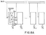
- Fig. 8A shows a device having a plurality pair of the through current block circuit 10 (20, 30) and the output buffer (Trl, Tr2). A plurality of data are outputted from terminals Pl to Pn at the same time.
- Fig. 9 is a circuit diagram showing the main part of an embodiment of the invention wherein the operation timings of output buffers OB are shifted. More in particular, an input terminal IN of an output buffer OB to be inputted with a signal (address/data signal) from a bus BUS, is connected to a delay circuit Dl (D2 to Dn) via an inverter IV6 and transistor Tr41. The output terminal of the delay circuit Dl is connected to the gate of a transistor Tr2, and via an inverter IV7 to the gate of a transistor Trl.
- the internal circuit of one output buffer OB is shown, the internal circuit of each of the other output buffers OB is substantially the same.
- the delay time of the delay circuit Dl to Dn in each output buffer OB is arranged to become slightly larger in the order recited.
- the timing signal T is outputted, it is applied to transistors 41 of the output buffers OB at the same time. Since the delay time of each delay circuit Dl to Dn is slightly different from each other, the output buffers OB sequentially start operating with a time difference, starting from the left side to the right side shown in Fig. 9. Accordingly, an output is delivered first at an output terminal Pl, then at an output terminal P2, and so on.
- Such a circuit arrangement allows to deal with a high operation frequency and make small a peak current flowing through the ground pin, thereby preventing a malfunction.
- the delay time of the delay circuit is changed for each output buffer as described above.
- the same delay time for a plurality of output buffers may also be used.
- the output terminals are divided into groups Pl to P4, P5 to P8, and so on each group containing four output terminals and having the same delay time.
- the delay circuit may be constructed of a plurality of serially connected inverters, a plurality of resistors, a plurality of capacitors, or a combination thereof.
- the size of a transistor constituting an inverter, the number of inverters to be connected, the value of a resistor, or the value of a capacitor is changed.
- the first circuit constructed of a combination of the delay circuit DL2 and three transistors Tr21 to Tr23 or the second circuit constructed of a combination of the delay circuit DL2 and three transistors Tr24 to Tr26 may be used as a circuit for delaying the leading edge or trailing edge of an input signal or as a noise eliminator circuit for eliminating noises superposed upon an input signal.
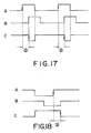
- the first circuit is shown in Fig. 15, and its equivalent circuit is shown in Fig. 13. The operation of this circuit is illustrated in Figs. 16 to 18.
- Fig. 16 illustrates a noise eliminating operation.
- a noise N is superposed on a signal at the input terminal IN.
- This noise N is transmitted to the transistor Tr21 so that its output becomes a high impedance state (tri-state) .
- This first circuit processes an internal signal so that its load is negligibly small, and the noise period (1) is short. Therefore, an output signal at the output terminal C takes a previous state of H level.
- the noise N is delayed by the delay circuit DL2 and reaches point B.
- the transistor Tr23 is off at this time so that the noise will not appear at the output terminal C.
- Figs. 17 and 18 illustrate a trailing edge delay operation. Although the high impedance state is retained at the output terminal C during the periods (2) and (3) respectively shown in Figs. 17 and 18, there is no problem during these periods (2) and (3) because of the same reason described with the period (1).
- the second circuit is shown in Fig. 21, and its equivalent circuit is shown in Fig. 19. The operation of this circuit is illustrated in Figs. 22 to 24.
- Fig. 22 illustrates a noise eliminating operation.
- a noise N is superposed on a signal at the input terminal IN.
- This noise N is transmitted to the transistor Tr26 so that its output becomes a high impedance state (tri-state).
- This second circuit processes an internal signal so that its load is negligibly small, and the noise period (4) is short. Therefore, an output signal at the output terminal C takes a previous state of L level.
- the noise N is delayed by the delay circuit DL2 and reaches point B.
- the transistor Tr24 is off at this time so that the noise will not appear at the output terminal C.
- Figs. 23 and 24 illustrate a trailing edge delay operation. Although the high impedance state is retained at the output terminal C during the periods (5) and (6) respectively shown in Figs. 23 and 24, there is no problem during these periods (5) and (6) because of the same reason described with the period (4).
- the number of transistors is reduced by one as compared with conventional circuits.
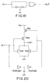
- the equivalent circuit shown in Fig. 13 of the circuit of Fig. 15 has been realized heretofore generally by the circuit shown in Fig. 14 which requires eight transistors Tr51 to Tr58.
- the embodiment circuit shown in Fig. 15 requires seven transistors Tr21 to Tr23, and Tr20a to Tr20d.
- the conventional circuit shown in Fig. 20 requires eight transistors Tr61 to Tr68
- the embodiment circuit shown in Fig. 21 requires seven transistors Tr24 to Tr26, and Tr20e to Tr20h.
Landscapes
- Engineering & Computer Science (AREA)
- Power Engineering (AREA)
- Physics & Mathematics (AREA)
- Computer Hardware Design (AREA)
- Computing Systems (AREA)
- General Engineering & Computer Science (AREA)
- Mathematical Physics (AREA)
- Logic Circuits (AREA)
- Static Random-Access Memory (AREA)
- Semiconductor Integrated Circuits (AREA)
- Electronic Switches (AREA)
- Dram (AREA)
Applications Claiming Priority (3)
| Application Number | Priority Date | Filing Date | Title |
|---|---|---|---|
| JP1324754A JPH03185921A (ja) | 1989-12-14 | 1989-12-14 | 半導体集積回路 |
| JP324754/89 | 1989-12-14 | ||
| EP90124192A EP0432790B1 (de) | 1989-12-14 | 1990-12-14 | Ausgangsdatenpufferschaltung für integrierte Halbleiterschaltung |
Related Parent Applications (1)
| Application Number | Title | Priority Date | Filing Date |
|---|---|---|---|
| EP90124192.7 Division | 1990-12-14 |
Publications (1)
| Publication Number | Publication Date |
|---|---|
| EP0686975A1 true EP0686975A1 (de) | 1995-12-13 |
Family
ID=18169307
Family Applications (2)
| Application Number | Title | Priority Date | Filing Date |
|---|---|---|---|
| EP95113987A Withdrawn EP0686975A1 (de) | 1989-12-14 | 1990-12-14 | Ausgangsdatenpufferschaltung für integrierte Halbleiterschaltung |
| EP90124192A Expired - Lifetime EP0432790B1 (de) | 1989-12-14 | 1990-12-14 | Ausgangsdatenpufferschaltung für integrierte Halbleiterschaltung |
Family Applications After (1)
| Application Number | Title | Priority Date | Filing Date |
|---|---|---|---|
| EP90124192A Expired - Lifetime EP0432790B1 (de) | 1989-12-14 | 1990-12-14 | Ausgangsdatenpufferschaltung für integrierte Halbleiterschaltung |
Country Status (5)
| Country | Link |
|---|---|
| US (1) | US5194764A (de) |
| EP (2) | EP0686975A1 (de) |
| JP (1) | JPH03185921A (de) |
| KR (1) | KR950001087B1 (de) |
| DE (1) | DE69028903D1 (de) |
Families Citing this family (28)
| Publication number | Priority date | Publication date | Assignee | Title |
|---|---|---|---|---|
| US5334889A (en) * | 1990-06-20 | 1994-08-02 | Oki Electric Industry, Co., Ltd. | CMOS output buffer circuit with less noise |
| US5491432A (en) * | 1992-08-07 | 1996-02-13 | Lsi Logic Corporation | CMOS Differential driver circuit for high offset ground |
| ATE135510T1 (de) * | 1992-09-18 | 1996-03-15 | Siemens Ag | Integrierte pufferschaltung |
| DE59207548D1 (de) * | 1992-09-18 | 1997-01-02 | Siemens Ag | Integrierte Pufferschaltung |
| US5604453A (en) * | 1993-04-23 | 1997-02-18 | Altera Corporation | Circuit for reducing ground bounce |
| DE4447546C2 (de) * | 1993-10-29 | 1996-06-27 | Mitsubishi Electric Corp | Integrierte Halbleiterschaltung |
| JPH07129538A (ja) * | 1993-10-29 | 1995-05-19 | Mitsubishi Denki Semiconductor Software Kk | 半導体集積回路 |
| US5721875A (en) * | 1993-11-12 | 1998-02-24 | Intel Corporation | I/O transceiver having a pulsed latch receiver circuit |
| JPH07182864A (ja) * | 1993-12-21 | 1995-07-21 | Mitsubishi Electric Corp | 半導体記憶装置 |
| JP2671787B2 (ja) * | 1993-12-24 | 1997-10-29 | 日本電気株式会社 | 出力バッファ回路 |
| DE4422784C2 (de) * | 1994-06-29 | 1999-05-27 | Texas Instruments Deutschland | Schaltungsanordnung mit wenigstens einer Schaltungseinheit wie einem Register, einer Speicherzelle, einer Speicheranordnung oder dergleichen |
| KR970005570B1 (ko) * | 1994-07-14 | 1997-04-17 | 현대전자산업 주식회사 | 데이타 출력버퍼 |
| KR0129592B1 (ko) * | 1994-09-09 | 1998-10-01 | 김주용 | 저잡음 출력 버퍼 |
| US5434519A (en) * | 1994-10-11 | 1995-07-18 | International Business Machines Corporation | Self-resetting CMOS off-chip driver |
| US5596284A (en) * | 1994-11-10 | 1997-01-21 | Brooktree Corporation | System for, and method of, minimizing noise in an integrated circuit chip |
| JPH08228141A (ja) * | 1995-02-21 | 1996-09-03 | Kawasaki Steel Corp | 出力バッファ回路 |
| US5539336A (en) * | 1995-05-01 | 1996-07-23 | Lsi Logic Corporation | High speed driver circuit with improved off transition feedback |
| US5825206A (en) * | 1996-08-14 | 1998-10-20 | Intel Corporation | Five volt safe output buffer circuit that controls the substrate and gates of the pull-up devices |
| US6097220A (en) | 1997-06-11 | 2000-08-01 | Intel Corporation | Method and circuit for recycling charge |
| KR100475046B1 (ko) * | 1998-07-20 | 2005-05-27 | 삼성전자주식회사 | 출력버퍼 및 그의 버퍼링 방법 |
| US6459313B1 (en) | 1998-09-18 | 2002-10-01 | Lsi Logic Corporation | IO power management: synchronously regulated output skew |
| US20030189448A1 (en) * | 2002-04-08 | 2003-10-09 | Silicon Video, Inc. | MOSFET inverter with controlled slopes and a method of making |
| US6724224B1 (en) * | 2003-04-07 | 2004-04-20 | Pericom Semiconductor Corp. | Bus relay and voltage shifter without direction control input |
| KR100842743B1 (ko) * | 2006-10-27 | 2008-07-01 | 주식회사 하이닉스반도체 | 고집적 반도체 장치 |
| JP5151413B2 (ja) | 2007-11-20 | 2013-02-27 | 富士通セミコンダクター株式会社 | データ保持回路 |
| CN105850043B (zh) * | 2013-12-27 | 2019-01-11 | 松下知识产权经营株式会社 | 半导体集成电路、锁存电路以及触发器 |
| KR102290384B1 (ko) * | 2015-02-16 | 2021-08-17 | 삼성전자주식회사 | 누설 전류 기반의 지연 회로 |
| CN105162442B (zh) * | 2015-10-08 | 2018-12-21 | 重庆中科芯亿达电子有限公司 | 一种功率管驱动集成电路 |
Citations (2)
| Publication number | Priority date | Publication date | Assignee | Title |
|---|---|---|---|---|
| US4556961A (en) * | 1981-05-26 | 1985-12-03 | Tokyo Shibaura Denki Kabushiki Kaisha | Semiconductor memory with delay means to reduce peak currents |
| EP0194939A2 (de) * | 1985-03-14 | 1986-09-17 | Fujitsu Limited | Halbleiterspeicheranordnung |
Family Cites Families (18)
| Publication number | Priority date | Publication date | Assignee | Title |
|---|---|---|---|---|
| CA945641A (en) * | 1970-04-27 | 1974-04-16 | Tokyo Shibaura Electric Co. | Logic circuit using complementary type insulated gate field effect transistors |
| JPS5787620A (en) * | 1980-11-20 | 1982-06-01 | Fujitsu Ltd | Clock generating circuit |
| JPS57168319A (en) * | 1981-04-09 | 1982-10-16 | Fujitsu Ltd | Parallel output buffer circuit |
| US4883986A (en) * | 1981-05-19 | 1989-11-28 | Tokyo Shibaura Denki Kabushiki Kaisha | High density semiconductor circuit using CMOS transistors |
| JPS5838032A (ja) * | 1981-08-13 | 1983-03-05 | Fujitsu Ltd | C―mosインバータ駆動用バッファ回路 |
| JPS59148426A (ja) * | 1983-02-15 | 1984-08-25 | Nec Corp | 同時動作タイミング制御回路 |
| JPS60130920A (ja) * | 1983-12-20 | 1985-07-12 | Nec Corp | 半導体集積論理回路 |
| US4786824A (en) * | 1984-05-24 | 1988-11-22 | Kabushiki Kaisha Toshiba | Input signal level detecting circuit |
| JPS61214817A (ja) * | 1985-03-20 | 1986-09-24 | Toshiba Corp | Cmos集積回路 |
| JPH07107978B2 (ja) * | 1985-11-07 | 1995-11-15 | ロ−ム株式会社 | C−mos回路 |
| US4882507B1 (en) * | 1987-07-31 | 1993-03-16 | Output circuit of semiconductor integrated circuit device | |
| US4857765A (en) * | 1987-11-17 | 1989-08-15 | International Business Machines Corporation | Noise control in an integrated circuit chip |
| US4992677A (en) * | 1988-03-23 | 1991-02-12 | Hitachi, Ltd. | High speed MOSFET output buffer with low noise |
| US4959563A (en) * | 1988-06-29 | 1990-09-25 | Texas Instruments Incorporated | Adjustable low noise output circuit |
| US4924120A (en) * | 1988-06-29 | 1990-05-08 | Texas Instruments Incorporated | Low noise output circuit |
| KR910004735B1 (ko) * | 1988-07-18 | 1991-07-10 | 삼성전자 주식회사 | 데이타 출력용 버퍼회로 |
| JPH0289292A (ja) * | 1988-09-26 | 1990-03-29 | Toshiba Corp | 半導体メモリ |
| US4975599A (en) * | 1989-07-26 | 1990-12-04 | International Business Machines Corporation | Method and resulting devices for compensating for process variables in a CMOS device driver circuit |
-
1989
- 1989-12-14 JP JP1324754A patent/JPH03185921A/ja active Pending
-
1990
- 1990-12-13 US US07/627,058 patent/US5194764A/en not_active Expired - Fee Related
- 1990-12-14 EP EP95113987A patent/EP0686975A1/de not_active Withdrawn
- 1990-12-14 KR KR1019900020570A patent/KR950001087B1/ko not_active Expired - Fee Related
- 1990-12-14 EP EP90124192A patent/EP0432790B1/de not_active Expired - Lifetime
- 1990-12-14 DE DE69028903T patent/DE69028903D1/de not_active Expired - Lifetime
Patent Citations (2)
| Publication number | Priority date | Publication date | Assignee | Title |
|---|---|---|---|---|
| US4556961A (en) * | 1981-05-26 | 1985-12-03 | Tokyo Shibaura Denki Kabushiki Kaisha | Semiconductor memory with delay means to reduce peak currents |
| EP0194939A2 (de) * | 1985-03-14 | 1986-09-17 | Fujitsu Limited | Halbleiterspeicheranordnung |
Also Published As
| Publication number | Publication date |
|---|---|
| EP0432790A2 (de) | 1991-06-19 |
| EP0432790A3 (en) | 1992-09-30 |
| KR950001087B1 (ko) | 1995-02-08 |
| US5194764A (en) | 1993-03-16 |
| DE69028903D1 (de) | 1996-11-21 |
| EP0432790B1 (de) | 1996-10-16 |
| JPH03185921A (ja) | 1991-08-13 |
| KR910013535A (ko) | 1991-08-08 |
Similar Documents
| Publication | Publication Date | Title |
|---|---|---|
| EP0686975A1 (de) | Ausgangsdatenpufferschaltung für integrierte Halbleiterschaltung | |
| EP0606912B1 (de) | CMOS Schaltungen zur Erzeugung mehrphasiger Taktsignalen | |
| IE53406B1 (en) | A buffer circuit including inverter circuitry | |
| US5825215A (en) | Output buffer circuit | |
| JP2003168969A (ja) | レベルシフト回路 | |
| EP0405833A2 (de) | Eingangspuffer mit programmierbarem Eingangsschaltpegel | |
| EP0477706B1 (de) | Schaltung zum Synchronisieren von asynchronen Zustandsmaschinen | |
| EP1406388B1 (de) | Integrierte Schaltungsanordnungen mit Dateninversion zur Verringerung von Störsignalen bei gleichzeitigem Schalten und Verschachtelung von Paralleldaten | |
| US6172516B1 (en) | Output buffering apparatus and method | |
| KR100211758B1 (ko) | 멀티 파워를 사용하는 데이터 출력버퍼 | |
| JPH06204823A (ja) | 補償回路と遅延を補償する方法 | |
| US6617881B2 (en) | Semiconductor integrated circuit | |
| US4761572A (en) | Semiconductor large scale integrated circuit with noise cut circuit | |
| US5739701A (en) | Input/output buffer circuit having reduced power consumption | |
| US7180326B2 (en) | Noise elimination circuit | |
| US11271549B2 (en) | Semiconductor device for controlling voltage at an input node of a circuit during a low power mode | |
| EP0107442A2 (de) | Signal-Eingangsschaltung | |
| US5715198A (en) | Output latching circuit for static memory devices | |
| KR19980058197A (ko) | 제어신호를 이용한 출력패드 회로 | |
| US6710638B2 (en) | Voltage conversion circuit and semiconductor device | |
| EP0311102B1 (de) | Halbleiter-IC mit einer Schaltung zur Vermeidung fehlerhafter Arbeitsweise, verursacht durch Speisespannungsströrungen | |
| US6005430A (en) | Clock skew circuit | |
| EP0772301A2 (de) | Schaltkreis zur Stabilisierung des Ausgangs einer Schaltung mit drei Zuständen | |
| US5495182A (en) | Fast-fully restoring polarity control circuit | |
| US6172527B1 (en) | Output circuit capable of reducing feedthrough current |
Legal Events
| Date | Code | Title | Description |
|---|---|---|---|
| PUAI | Public reference made under article 153(3) epc to a published international application that has entered the european phase |
Free format text: ORIGINAL CODE: 0009012 |
|
| 17P | Request for examination filed |
Effective date: 19950906 |
|
| AC | Divisional application: reference to earlier application |
Ref document number: 432790 Country of ref document: EP |
|
| AK | Designated contracting states |
Kind code of ref document: A1 Designated state(s): DE FR GB |
|
| RIN1 | Information on inventor provided before grant (corrected) |
Inventor name: KAJI, MICHIO Inventor name: IWASHITA, MASAKAZU Inventor name: GOTOU, MASAKAZU Inventor name: ATOH, MASAMI Inventor name: MIYAWAKI, TSUKASA Inventor name: YANO, JUNJI |
|
| STAA | Information on the status of an ep patent application or granted ep patent |
Free format text: STATUS: THE APPLICATION HAS BEEN WITHDRAWN |
|
| 18W | Application withdrawn |
Withdrawal date: 19960813 |