EP0687961A1 - Druckplatte und Verfahren zu deren Herstellung - Google Patents
Druckplatte und Verfahren zu deren Herstellung Download PDFInfo
- Publication number
- EP0687961A1 EP0687961A1 EP95108144A EP95108144A EP0687961A1 EP 0687961 A1 EP0687961 A1 EP 0687961A1 EP 95108144 A EP95108144 A EP 95108144A EP 95108144 A EP95108144 A EP 95108144A EP 0687961 A1 EP0687961 A1 EP 0687961A1
- Authority
- EP
- European Patent Office
- Prior art keywords
- printing plate
- substrate
- layer
- type photoconductor
- ink
- Prior art date
- Legal status (The legal status is an assumption and is not a legal conclusion. Google has not performed a legal analysis and makes no representation as to the accuracy of the status listed.)
- Granted
Links
- 238000007639 printing Methods 0.000 title claims abstract description 361
- 238000004519 manufacturing process Methods 0.000 title claims abstract description 55
- 239000000758 substrate Substances 0.000 claims abstract description 230
- 238000004070 electrodeposition Methods 0.000 claims abstract description 206
- 239000002659 electrodeposit Substances 0.000 claims abstract description 144
- 239000000463 material Substances 0.000 claims abstract description 68
- 230000003287 optical effect Effects 0.000 claims abstract description 54
- 238000010438 heat treatment Methods 0.000 claims abstract description 24
- 238000005406 washing Methods 0.000 claims abstract description 24
- 238000001035 drying Methods 0.000 claims abstract description 21
- 229920000620 organic polymer Polymers 0.000 claims abstract description 13
- 238000009877 rendering Methods 0.000 claims abstract description 13
- 238000000034 method Methods 0.000 claims description 54
- 239000005871 repellent Substances 0.000 claims description 53
- XLYOFNOQVPJJNP-UHFFFAOYSA-N water Substances O XLYOFNOQVPJJNP-UHFFFAOYSA-N 0.000 claims description 48
- 230000008569 process Effects 0.000 claims description 33
- 238000001459 lithography Methods 0.000 claims description 22
- 238000012546 transfer Methods 0.000 claims description 20
- 238000012216 screening Methods 0.000 claims description 13
- 230000001965 increasing effect Effects 0.000 claims description 6
- 239000010410 layer Substances 0.000 description 195
- 238000002360 preparation method Methods 0.000 description 39
- 239000011248 coating agent Substances 0.000 description 32
- 238000000576 coating method Methods 0.000 description 32
- XLOMVQKBTHCTTD-UHFFFAOYSA-N Zinc monoxide Chemical compound [Zn]=O XLOMVQKBTHCTTD-UHFFFAOYSA-N 0.000 description 29
- 229910052782 aluminium Inorganic materials 0.000 description 28
- 239000004065 semiconductor Substances 0.000 description 28
- XAGFODPZIPBFFR-UHFFFAOYSA-N aluminium Chemical compound [Al] XAGFODPZIPBFFR-UHFFFAOYSA-N 0.000 description 26
- 239000000203 mixture Substances 0.000 description 25
- 238000011161 development Methods 0.000 description 23
- 229920005989 resin Polymers 0.000 description 19
- 239000011347 resin Substances 0.000 description 19
- YXFVVABEGXRONW-UHFFFAOYSA-N Toluene Chemical compound CC1=CC=CC=C1 YXFVVABEGXRONW-UHFFFAOYSA-N 0.000 description 18
- 230000000694 effects Effects 0.000 description 17
- 239000010949 copper Substances 0.000 description 14
- 239000011787 zinc oxide Substances 0.000 description 14
- 238000007645 offset printing Methods 0.000 description 13
- 239000000243 solution Substances 0.000 description 13
- 125000002091 cationic group Chemical group 0.000 description 12
- 229910052751 metal Inorganic materials 0.000 description 12
- 239000002184 metal Substances 0.000 description 12
- 239000004925 Acrylic resin Substances 0.000 description 11
- 229920000178 Acrylic resin Polymers 0.000 description 11
- 239000000049 pigment Substances 0.000 description 10
- 239000002861 polymer material Substances 0.000 description 10
- IUVCFHHAEHNCFT-INIZCTEOSA-N 2-[(1s)-1-[4-amino-3-(3-fluoro-4-propan-2-yloxyphenyl)pyrazolo[3,4-d]pyrimidin-1-yl]ethyl]-6-fluoro-3-(3-fluorophenyl)chromen-4-one Chemical compound C1=C(F)C(OC(C)C)=CC=C1C(C1=C(N)N=CN=C11)=NN1[C@@H](C)C1=C(C=2C=C(F)C=CC=2)C(=O)C2=CC(F)=CC=C2O1 IUVCFHHAEHNCFT-INIZCTEOSA-N 0.000 description 9
- QTBSBXVTEAMEQO-UHFFFAOYSA-N Acetic acid Chemical compound CC(O)=O QTBSBXVTEAMEQO-UHFFFAOYSA-N 0.000 description 9
- KFZMGEQAYNKOFK-UHFFFAOYSA-N Isopropanol Chemical compound CC(C)O KFZMGEQAYNKOFK-UHFFFAOYSA-N 0.000 description 9
- GWEVSGVZZGPLCZ-UHFFFAOYSA-N Titan oxide Chemical compound O=[Ti]=O GWEVSGVZZGPLCZ-UHFFFAOYSA-N 0.000 description 9
- 230000008901 benefit Effects 0.000 description 9
- 229920006267 polyester film Polymers 0.000 description 9
- 229920001296 polysiloxane Polymers 0.000 description 9
- 230000002829 reductive effect Effects 0.000 description 9
- XKRFYHLGVUSROY-UHFFFAOYSA-N Argon Chemical compound [Ar] XKRFYHLGVUSROY-UHFFFAOYSA-N 0.000 description 8
- 230000015572 biosynthetic process Effects 0.000 description 8
- ZNQVEEAIQZEUHB-UHFFFAOYSA-N 2-ethoxyethanol Chemical compound CCOCCO ZNQVEEAIQZEUHB-UHFFFAOYSA-N 0.000 description 7
- 239000003795 chemical substances by application Substances 0.000 description 7
- 238000000151 deposition Methods 0.000 description 7
- 230000008021 deposition Effects 0.000 description 7
- 239000002245 particle Substances 0.000 description 7
- 230000009467 reduction Effects 0.000 description 7
- PXHVJJICTQNCMI-UHFFFAOYSA-N nickel Substances [Ni] PXHVJJICTQNCMI-UHFFFAOYSA-N 0.000 description 6
- 239000003921 oil Substances 0.000 description 6
- OKTJSMMVPCPJKN-UHFFFAOYSA-N Carbon Chemical compound [C] OKTJSMMVPCPJKN-UHFFFAOYSA-N 0.000 description 5
- 230000001070 adhesive effect Effects 0.000 description 5
- 229910052799 carbon Inorganic materials 0.000 description 5
- 238000006243 chemical reaction Methods 0.000 description 5
- 238000001723 curing Methods 0.000 description 5
- 239000006185 dispersion Substances 0.000 description 5
- QSHDDOUJBYECFT-UHFFFAOYSA-N mercury Chemical compound [Hg] QSHDDOUJBYECFT-UHFFFAOYSA-N 0.000 description 5
- 229910052753 mercury Inorganic materials 0.000 description 5
- 238000007747 plating Methods 0.000 description 5
- BASFCYQUMIYNBI-UHFFFAOYSA-N platinum Substances [Pt] BASFCYQUMIYNBI-UHFFFAOYSA-N 0.000 description 5
- 230000035945 sensitivity Effects 0.000 description 5
- 229920003048 styrene butadiene rubber Polymers 0.000 description 5
- OGIDPMRJRNCKJF-UHFFFAOYSA-N titanium oxide Inorganic materials [Ti]=O OGIDPMRJRNCKJF-UHFFFAOYSA-N 0.000 description 5
- 229910052786 argon Inorganic materials 0.000 description 4
- 229910052802 copper Inorganic materials 0.000 description 4
- 239000003822 epoxy resin Substances 0.000 description 4
- 229920002313 fluoropolymer Polymers 0.000 description 4
- 239000004811 fluoropolymer Substances 0.000 description 4
- -1 for example Substances 0.000 description 4
- 229910052759 nickel Inorganic materials 0.000 description 4
- 238000000016 photochemical curing Methods 0.000 description 4
- 229920000647 polyepoxide Polymers 0.000 description 4
- 239000000047 product Substances 0.000 description 4
- 229930187593 rose bengal Natural products 0.000 description 4
- AZJPTIGZZTZIDR-UHFFFAOYSA-L rose bengal Chemical compound [K+].[K+].[O-]C(=O)C1=C(Cl)C(Cl)=C(Cl)C(Cl)=C1C1=C2C=C(I)C(=O)C(I)=C2OC2=C(I)C([O-])=C(I)C=C21 AZJPTIGZZTZIDR-UHFFFAOYSA-L 0.000 description 4
- 229940081623 rose bengal Drugs 0.000 description 4
- STRXNPAVPKGJQR-UHFFFAOYSA-N rose bengal A Natural products O1C(=O)C(C(=CC=C2Cl)Cl)=C2C21C1=CC(I)=C(O)C(I)=C1OC1=C(I)C(O)=C(I)C=C21 STRXNPAVPKGJQR-UHFFFAOYSA-N 0.000 description 4
- GGCZERPQGJTIQP-UHFFFAOYSA-N sodium;9,10-dioxoanthracene-2-sulfonic acid Chemical compound [Na+].C1=CC=C2C(=O)C3=CC(S(=O)(=O)O)=CC=C3C(=O)C2=C1 GGCZERPQGJTIQP-UHFFFAOYSA-N 0.000 description 4
- 239000007787 solid Substances 0.000 description 4
- XOLBLPGZBRYERU-UHFFFAOYSA-N tin dioxide Chemical compound O=[Sn]=O XOLBLPGZBRYERU-UHFFFAOYSA-N 0.000 description 4
- 206010034972 Photosensitivity reaction Diseases 0.000 description 3
- 239000005062 Polybutadiene Substances 0.000 description 3
- 239000004809 Teflon Substances 0.000 description 3
- 229920006362 Teflon® Polymers 0.000 description 3
- 238000005299 abrasion Methods 0.000 description 3
- 239000000853 adhesive Substances 0.000 description 3
- 125000000129 anionic group Chemical group 0.000 description 3
- 239000011247 coating layer Substances 0.000 description 3
- XCJYREBRNVKWGJ-UHFFFAOYSA-N copper(II) phthalocyanine Chemical compound [Cu+2].C12=CC=CC=C2C(N=C2[N-]C(C3=CC=CC=C32)=N2)=NC1=NC([C]1C=CC=CC1=1)=NC=1N=C1[C]3C=CC=CC3=C2[N-]1 XCJYREBRNVKWGJ-UHFFFAOYSA-N 0.000 description 3
- 238000007772 electroless plating Methods 0.000 description 3
- 239000008206 lipophilic material Substances 0.000 description 3
- 230000036211 photosensitivity Effects 0.000 description 3
- 229910052697 platinum Inorganic materials 0.000 description 3
- 229920002037 poly(vinyl butyral) polymer Polymers 0.000 description 3
- 229920002857 polybutadiene Polymers 0.000 description 3
- 239000000843 powder Substances 0.000 description 3
- 239000011369 resultant mixture Substances 0.000 description 3
- 230000001235 sensitizing effect Effects 0.000 description 3
- 239000010936 titanium Substances 0.000 description 3
- 229910052719 titanium Inorganic materials 0.000 description 3
- WFKWXMTUELFFGS-UHFFFAOYSA-N tungsten Chemical compound [W] WFKWXMTUELFFGS-UHFFFAOYSA-N 0.000 description 3
- 229910052721 tungsten Inorganic materials 0.000 description 3
- 239000010937 tungsten Substances 0.000 description 3
- 229910052725 zinc Inorganic materials 0.000 description 3
- 239000011701 zinc Substances 0.000 description 3
- LVGUZGTVOIAKKC-UHFFFAOYSA-N 1,1,1,2-tetrafluoroethane Chemical compound FCC(F)(F)F LVGUZGTVOIAKKC-UHFFFAOYSA-N 0.000 description 2
- OZAIFHULBGXAKX-UHFFFAOYSA-N 2-(2-cyanopropan-2-yldiazenyl)-2-methylpropanenitrile Chemical compound N#CC(C)(C)N=NC(C)(C)C#N OZAIFHULBGXAKX-UHFFFAOYSA-N 0.000 description 2
- SOGAXMICEFXMKE-UHFFFAOYSA-N Butylmethacrylate Chemical compound CCCCOC(=O)C(C)=C SOGAXMICEFXMKE-UHFFFAOYSA-N 0.000 description 2
- 229910021578 Iron(III) chloride Inorganic materials 0.000 description 2
- RTAQQCXQSZGOHL-UHFFFAOYSA-N Titanium Chemical compound [Ti] RTAQQCXQSZGOHL-UHFFFAOYSA-N 0.000 description 2
- NIXOWILDQLNWCW-UHFFFAOYSA-N acrylic acid group Chemical group C(C=C)(=O)O NIXOWILDQLNWCW-UHFFFAOYSA-N 0.000 description 2
- 229920000180 alkyd Polymers 0.000 description 2
- 239000000956 alloy Substances 0.000 description 2
- 229910045601 alloy Inorganic materials 0.000 description 2
- 239000011230 binding agent Substances 0.000 description 2
- 239000001055 blue pigment Substances 0.000 description 2
- 239000006229 carbon black Substances 0.000 description 2
- 238000004040 coloring Methods 0.000 description 2
- 239000002131 composite material Substances 0.000 description 2
- 239000004020 conductor Substances 0.000 description 2
- 239000000470 constituent Substances 0.000 description 2
- 230000035613 defoliation Effects 0.000 description 2
- 238000013461 design Methods 0.000 description 2
- 230000002708 enhancing effect Effects 0.000 description 2
- 238000005530 etching Methods 0.000 description 2
- 239000003925 fat Substances 0.000 description 2
- 239000000945 filler Substances 0.000 description 2
- 239000011888 foil Substances 0.000 description 2
- 238000013007 heat curing Methods 0.000 description 2
- 230000005660 hydrophilic surface Effects 0.000 description 2
- 230000006872 improvement Effects 0.000 description 2
- 229920000831 ionic polymer Polymers 0.000 description 2
- RBTARNINKXHZNM-UHFFFAOYSA-K iron trichloride Chemical compound Cl[Fe](Cl)Cl RBTARNINKXHZNM-UHFFFAOYSA-K 0.000 description 2
- 239000012948 isocyanate Substances 0.000 description 2
- 150000002513 isocyanates Chemical class 0.000 description 2
- 239000007788 liquid Substances 0.000 description 2
- 230000007246 mechanism Effects 0.000 description 2
- 230000003446 memory effect Effects 0.000 description 2
- 238000002156 mixing Methods 0.000 description 2
- 238000012986 modification Methods 0.000 description 2
- 230000004048 modification Effects 0.000 description 2
- 230000001590 oxidative effect Effects 0.000 description 2
- 238000003909 pattern recognition Methods 0.000 description 2
- 230000002688 persistence Effects 0.000 description 2
- 108091008695 photoreceptors Proteins 0.000 description 2
- 229920000642 polymer Polymers 0.000 description 2
- 239000002244 precipitate Substances 0.000 description 2
- 238000012545 processing Methods 0.000 description 2
- 238000011084 recovery Methods 0.000 description 2
- 239000012266 salt solution Substances 0.000 description 2
- 229920002050 silicone resin Polymers 0.000 description 2
- 229910052709 silver Inorganic materials 0.000 description 2
- 239000010944 silver (metal) Substances 0.000 description 2
- 229910001220 stainless steel Inorganic materials 0.000 description 2
- 239000010935 stainless steel Substances 0.000 description 2
- 239000011550 stock solution Substances 0.000 description 2
- 239000011135 tin Substances 0.000 description 2
- DPBJAVGHACCNRL-UHFFFAOYSA-N 2-(dimethylamino)ethyl prop-2-enoate Chemical compound CN(C)CCOC(=O)C=C DPBJAVGHACCNRL-UHFFFAOYSA-N 0.000 description 1
- VHUUQVKOLVNVRT-UHFFFAOYSA-N Ammonium hydroxide Chemical compound [NH4+].[OH-] VHUUQVKOLVNVRT-UHFFFAOYSA-N 0.000 description 1
- RYGMFSIKBFXOCR-UHFFFAOYSA-N Copper Chemical compound [Cu] RYGMFSIKBFXOCR-UHFFFAOYSA-N 0.000 description 1
- WOBHKFSMXKNTIM-UHFFFAOYSA-N Hydroxyethyl methacrylate Chemical compound CC(=C)C(=O)OCCO WOBHKFSMXKNTIM-UHFFFAOYSA-N 0.000 description 1
- 229920000877 Melamine resin Polymers 0.000 description 1
- 239000004640 Melamine resin Substances 0.000 description 1
- VVQNEPGJFQJSBK-UHFFFAOYSA-N Methyl methacrylate Chemical compound COC(=O)C(C)=C VVQNEPGJFQJSBK-UHFFFAOYSA-N 0.000 description 1
- 239000004952 Polyamide Substances 0.000 description 1
- HCHKCACWOHOZIP-UHFFFAOYSA-N Zinc Chemical compound [Zn] HCHKCACWOHOZIP-UHFFFAOYSA-N 0.000 description 1
- RGTGNSLGFMHBDM-UHFFFAOYSA-J [Zn++].[Cd++].[O-]S([O-])(=O)=O.[O-]S([O-])(=O)=O Chemical compound [Zn++].[Cd++].[O-]S([O-])(=O)=O.[O-]S([O-])(=O)=O RGTGNSLGFMHBDM-UHFFFAOYSA-J 0.000 description 1
- UKLDJPRMSDWDSL-UHFFFAOYSA-L [dibutyl(dodecanoyloxy)stannyl] dodecanoate Chemical compound CCCCCCCCCCCC(=O)O[Sn](CCCC)(CCCC)OC(=O)CCCCCCCCCCC UKLDJPRMSDWDSL-UHFFFAOYSA-L 0.000 description 1
- 238000010521 absorption reaction Methods 0.000 description 1
- 125000003647 acryloyl group Chemical group O=C([*])C([H])=C([H])[H] 0.000 description 1
- 150000001413 amino acids Chemical class 0.000 description 1
- QGZKDVFQNNGYKY-UHFFFAOYSA-N ammonia Natural products N QGZKDVFQNNGYKY-UHFFFAOYSA-N 0.000 description 1
- 150000001450 anions Chemical class 0.000 description 1
- 238000002048 anodisation reaction Methods 0.000 description 1
- 238000007664 blowing Methods 0.000 description 1
- UDSAIICHUKSCKT-UHFFFAOYSA-N bromophenol blue Chemical compound C1=C(Br)C(O)=C(Br)C=C1C1(C=2C=C(Br)C(O)=C(Br)C=2)C2=CC=CC=C2S(=O)(=O)O1 UDSAIICHUKSCKT-UHFFFAOYSA-N 0.000 description 1
- CQEYYJKEWSMYFG-UHFFFAOYSA-N butyl acrylate Chemical compound CCCCOC(=O)C=C CQEYYJKEWSMYFG-UHFFFAOYSA-N 0.000 description 1
- QHIWVLPBUQWDMQ-UHFFFAOYSA-N butyl prop-2-enoate;methyl 2-methylprop-2-enoate;prop-2-enoic acid Chemical compound OC(=O)C=C.COC(=O)C(C)=C.CCCCOC(=O)C=C QHIWVLPBUQWDMQ-UHFFFAOYSA-N 0.000 description 1
- 150000001768 cations Chemical class 0.000 description 1
- 229910052804 chromium Inorganic materials 0.000 description 1
- 239000011651 chromium Substances 0.000 description 1
- 239000003086 colorant Substances 0.000 description 1
- 238000009500 colour coating Methods 0.000 description 1
- 238000010276 construction Methods 0.000 description 1
- 238000007796 conventional method Methods 0.000 description 1
- 238000003851 corona treatment Methods 0.000 description 1
- 125000004122 cyclic group Chemical group 0.000 description 1
- 239000008367 deionised water Substances 0.000 description 1
- 229910021641 deionized water Inorganic materials 0.000 description 1
- 238000010586 diagram Methods 0.000 description 1
- 239000012975 dibutyltin dilaurate Substances 0.000 description 1
- PEVJCYPAFCUXEZ-UHFFFAOYSA-J dicopper;phosphonato phosphate Chemical compound [Cu+2].[Cu+2].[O-]P([O-])(=O)OP([O-])([O-])=O PEVJCYPAFCUXEZ-UHFFFAOYSA-J 0.000 description 1
- 238000010017 direct printing Methods 0.000 description 1
- 208000028659 discharge Diseases 0.000 description 1
- 238000010828 elution Methods 0.000 description 1
- 238000004945 emulsification Methods 0.000 description 1
- 238000002474 experimental method Methods 0.000 description 1
- 239000010408 film Substances 0.000 description 1
- 230000006870 function Effects 0.000 description 1
- 239000007789 gas Substances 0.000 description 1
- 239000011521 glass Substances 0.000 description 1
- LNEPOXFFQSENCJ-UHFFFAOYSA-N haloperidol Chemical compound C1CC(O)(C=2C=CC(Cl)=CC=2)CCN1CCCC(=O)C1=CC=C(F)C=C1 LNEPOXFFQSENCJ-UHFFFAOYSA-N 0.000 description 1
- 229910001385 heavy metal Inorganic materials 0.000 description 1
- 229920001477 hydrophilic polymer Polymers 0.000 description 1
- 230000002209 hydrophobic effect Effects 0.000 description 1
- AMGQUBHHOARCQH-UHFFFAOYSA-N indium;oxotin Chemical compound [In].[Sn]=O AMGQUBHHOARCQH-UHFFFAOYSA-N 0.000 description 1
- 229910052742 iron Inorganic materials 0.000 description 1
- XEEYBQQBJWHFJM-UHFFFAOYSA-N iron Substances [Fe] XEEYBQQBJWHFJM-UHFFFAOYSA-N 0.000 description 1
- 150000002739 metals Chemical class 0.000 description 1
- 239000011259 mixed solution Substances 0.000 description 1
- 229910001453 nickel ion Inorganic materials 0.000 description 1
- 239000011368 organic material Substances 0.000 description 1
- 230000002085 persistent effect Effects 0.000 description 1
- IEQIEDJGQAUEQZ-UHFFFAOYSA-N phthalocyanine Chemical compound N1C(N=C2C3=CC=CC=C3C(N=C3C4=CC=CC=C4C(=N4)N3)=N2)=C(C=CC=C2)C2=C1N=C1C2=CC=CC=C2C4=N1 IEQIEDJGQAUEQZ-UHFFFAOYSA-N 0.000 description 1
- 239000004033 plastic Substances 0.000 description 1
- 229920003023 plastic Polymers 0.000 description 1
- 229920002647 polyamide Polymers 0.000 description 1
- 229920006122 polyamide resin Polymers 0.000 description 1
- 229920000728 polyester Polymers 0.000 description 1
- 229920001225 polyester resin Polymers 0.000 description 1
- 239000004645 polyester resin Substances 0.000 description 1
- 229920005596 polymer binder Polymers 0.000 description 1
- 239000002491 polymer binding agent Substances 0.000 description 1
- 238000006116 polymerization reaction Methods 0.000 description 1
- 229920001343 polytetrafluoroethylene Polymers 0.000 description 1
- 239000004810 polytetrafluoroethylene Substances 0.000 description 1
- 230000001105 regulatory effect Effects 0.000 description 1
- 150000003839 salts Chemical class 0.000 description 1
- 238000004904 shortening Methods 0.000 description 1
- 230000003595 spectral effect Effects 0.000 description 1
- 239000004094 surface-active agent Substances 0.000 description 1
- RYCLIXPGLDDLTM-UHFFFAOYSA-J tetrapotassium;phosphonato phosphate Chemical compound [K+].[K+].[K+].[K+].[O-]P([O-])(=O)OP([O-])([O-])=O RYCLIXPGLDDLTM-UHFFFAOYSA-J 0.000 description 1
- 229910052718 tin Inorganic materials 0.000 description 1
- 235000010215 titanium dioxide Nutrition 0.000 description 1
- 239000012463 white pigment Substances 0.000 description 1
- NWJUKFMMXJODIL-UHFFFAOYSA-N zinc cadmium(2+) selenium(2-) Chemical compound [Zn+2].[Se-2].[Se-2].[Cd+2] NWJUKFMMXJODIL-UHFFFAOYSA-N 0.000 description 1
Images


Classifications
-
- G—PHYSICS
- G03—PHOTOGRAPHY; CINEMATOGRAPHY; ANALOGOUS TECHNIQUES USING WAVES OTHER THAN OPTICAL WAVES; ELECTROGRAPHY; HOLOGRAPHY
- G03G—ELECTROGRAPHY; ELECTROPHOTOGRAPHY; MAGNETOGRAPHY
- G03G13/00—Electrographic processes using a charge pattern
- G03G13/26—Electrographic processes using a charge pattern for the production of printing plates for non-xerographic printing processes
- G03G13/28—Planographic printing plates
- G03G13/286—Planographic printing plates for dry lithography
-
- G—PHYSICS
- G03—PHOTOGRAPHY; CINEMATOGRAPHY; ANALOGOUS TECHNIQUES USING WAVES OTHER THAN OPTICAL WAVES; ELECTROGRAPHY; HOLOGRAPHY
- G03G—ELECTROGRAPHY; ELECTROPHOTOGRAPHY; MAGNETOGRAPHY
- G03G17/00—Electrographic processes using patterns other than charge patterns, e.g. an electric conductivity pattern; Processes involving a migration, e.g. photoelectrophoresis, photoelectrosolography; Processes involving a selective transfer, e.g. electrophoto-adhesive processes; Apparatus essentially involving a single such process
- G03G17/02—Electrographic processes using patterns other than charge patterns, e.g. an electric conductivity pattern; Processes involving a migration, e.g. photoelectrophoresis, photoelectrosolography; Processes involving a selective transfer, e.g. electrophoto-adhesive processes; Apparatus essentially involving a single such process with electrolytic development
Definitions
- the present invention relates to a process for preparing a printing plate and a printing plate produced by said process. More particularly, the present invention relates to a process for preparing a printing plate using an N-type photoconductor layer having an optical memory property and a printing plate produced using the printing plate preparation process.
- a process commonly used in the art comprises coating a photosensitive resin on an aluminum plate or a zinc plate, bringing the coated plate into close contact with a photographic original plate having a desired pattern, and conducting exposure and development.
- a plate product of an aluminum plate bearing thereon a previously coated photosensitive resin has become commercially available as a PS (presensitized plate), and the exposure in a desired pattern of the PS plate followed by development to prepare a printing plate has spread in the art.
- an electrophotographic plate preparation process which can simply prepare an ink-receptive toner image on the printing plate, has been developed wherein the surface of a photoconductor or an organic photoconductor substrate is subjected to corona discharge treatment in a dark place and then exposure and toner development (dry powder development, wet liquid development, or the like) to form a toner image on the surface of the photoconductor substrate.
- an electrophotographic plate preparation process utilizing the properties of an oxide photoconductor, particularly zinc oxide (ZnO), photoconductor substrate prepared by coating the surface of a conductive substrate with a coating prepared by dispersing a fine powder of ZnO in a polymer binder and then drying the resultant coating is subjected to a series of the above steps of corona discharge, exposure, and toner development to prepare a printing plate.
- ZnO zinc oxide
- This process is advantageous in that all the plate preparation operations can be carried out in a dry state. Since ZnO is inherently hydrophilic, it has good wettability by dampening water used in offset printing, rendering the printing plate prepared by the above process suitable for offset printing.
- OPC organic photoconductor
- the currently most popular PS plate has gained public favor in that the resolution and durability are excellent and good print quality can be attained.
- the PS plate is disadvantageous in that it is expensive and has unsatisfactory photosensitivity (low sensitivity) in a novel exposing method, wherein optical drawing is carried out at a high speed, is not always compatible with the digital printing plate preparation process being in the course of development in recent years.
- Efforts have, of course, been made to increase the sensitivity of the photosensitive resin used in the PS plate to such an extent that the PS plate becomes suitable for laser digital plate preparation. The sensitivity, however, could not have been increased to that of the electrophotographic printing plate preparation process.
- a printing plate prepared by an electrophotographic plate preparation process utilizing an oxide photoconductor can be prepared at low cost by using a conductive paper substrate or the like and has been used extensively in the field of simple printing by taking advantage of dry developer. In general, however, this printing plate has low resolution and cannot be applied to high-quality printing and printing in large volumes.
- the use of liquid developer can improve the resolution as compared with the use of dry developer. Since, however, the plate wear is substantially the same, the use in printing in large volumes is impossible.
- the printing plate prepared by the above electrophotographic printing plate preparation process utilizing the organic photoconductor (OPC) has a plate wear of 100000 to 200000 sheets.
- OPC organic photoconductor
- the OPC layer at the non-image area should be dissolved away with the toner image being used as an etching resist to expose the hydrophilic surface of the substrate. This operation deteriorates the high resolution attained by the wet development, and the resultant printing plate generally has such a resolution as will be applicable to printing for newspaper (100 to 133 lines/in.) but could not have been put to practical use for high-quality printing (not less than 175 to 300 lines/in.).
- an N-type photoconductor layer formed on an N-type photoconductor substrate using a substrate having a conductive surface is exposed in a desired pattern by batch exposure and/or photo-drawing exposure, electrical conductivity is developed and persistent memory (optical memory) occurs.
- An ink-receptive component is electrochemically deposited (electrodeposited) on the exposed area to prepare an electrodeposited substrate.
- the electrodeposited substrate as such, is used as a printing plate.
- the ink-receptive component of the electrodeposited substrate is transferred onto a substrate for a printing plate to prepare a printing plate having an ink-receptive area.
- the above process can simply prepare a printing plate which can provide high-quality prints with high plate wear. Further, since photo-drawing can be used in the process, the process can be simplified, resulting in lowered production cost.
- the following three types of printing plate preparation processes can be provided by taking advantage of the optical memory property.
- an object of the present invention is to provide a printing plate, which can provide high-quality prints and high plate wear, and a printing plate preparation process which can prepare such a printing plate in a simple manner, enabling a reduction in and simplification of steps involved in the printing plate preparation, an improvement in reliability of the operation, a reduction in cost, and the use of photo-drawing.
- the process for preparing a printing plate according to the first invention comprises the steps of: providing an N-type photoconductor layer having an optical memory property on the surface of a substrate having an electrical conductivity at least in its surface to form an N-type photoconductor substrate; subjecting the N-type photoconductor layer to a desired pattern-wise exposure by batch exposure and/or photo-drawing exposure to render exposed areas electrically conductive; immersing the N-type photoconductor substrate in an electrodeposition bath to electrodeposit an ionic organic polymer contained in the electrodeposition bath to form an electrodeposit layer; and washing and drying the electrodeposited substrate which, as such, is to be used as a printing plate.
- the printing plate of the present invention comprises: an N-type photoconductor substrate formed by providing an N-type photoconductor layer having an optical memory property on the surface of a substrate having an electrical conductivity at least in its surface; and either or both of a lipophilic area and an oil-repellent area which has been electrodeposited pattern-wise on the surface of the N-type photoconductor layer.
- the N-type photoconductor layer formed on an N-type photoconductor substrate is subjected to a desired pattern-wise exposure by batch exposure and/or photo-drawing exposure to render exposed areas electrically conductive, and an ionic organic polymer contained in an electrodeposition bath is electrodeposited on the exposed areas to form an electrodeposit layer, thereby preparing a printing plate.
- a printing plate which can provide high-quality prints with high plate wear con be prepared in a simple manner.
- photo-drawing can be used in the process, the process can be simplified, resulting in lowered production cost.
- the second aspect of the present invention is accomplished by utilizing the first aspect of the present invention.
- the process for preparing a printing plate according to the second aspect comprises the steps of: providing an N-type photoconductor layer having an optical memory property on the surface of a substrate having an electrical conductivity at least in its surface to form an N-type photoconductor substrate; subjecting the N-type photoconductor layer to a desired pattern-wise exposure by batch exposure and/or photo-drawing exposure to render exposed areas electrically conductive; immersing the N-type photoconductor substrate in an electrodeposition bath to electrodeposit an ink-receptive component on the exposed areas; washing and drying the electrodeposited substrate; and transferring the ink-receptive component present on the N-type photoconductor layer onto a substrate for a printing plate.
- a printing plate comprising a substrate for a printing plate and, formed thereon by the above process, an ink-receptive area comprising an ink-receptive component.
- the third aspect of the present invention relates to a process for preparing a printing plate by taking advantage of light and heat.
- the development of electrical conductivity by exposure and the erase of the electrical conductivity by heating are carried out with respect to an N-type photoconductor layer, and an electrodeposition material is electrodeposited on the remaining conductive areas to provide a printing plate for wet printing or dry printing.
- the process for preparing a printing plate according to the present invention basically comprises utilizing the optical memory of an photoconductor, and an ionic organic polymer contained in an electrodeposition bath is electrodeposited on the optical memory area to prepare a printing plate.
- the electrodeposit layer formed by the electrodeposition is ink-receptive or ink-unreceptive depending upon the electrodeposition material used.
- the photoconductor as the photosensitive material used in the present invention is an optical memory N-type photoconductor having such a capability that, after exposure, the exposure effect can be stored for a long period of time.
- the light irradiation causes the electronic conduction to be increased in the exposed area, so that the electrical conductivity of the negative charge in the exposed area becomes much higher than the unexposed area. Consequently, depending upon the construction of the semiconductor material, the unexposed area has an electrical insulating property with the exposed area becoming electrically conductive. That is, the light irradiation enables one semiconductor surface to be divided into a conductive area and an insulating area. Such a principle has already been utilized in electrophotography.
- a certain N-type photoconductor has an optical memory property such that the light irradiation effect (exposure effect) can be stored for a certain period of time.
- This optical memory property is not permanent but kept for a period of time which varies depending upon the material used. It disappears after the given period of time, and the insulating property is recovered. The time taken for the recovery can be markedly shortened by suitable heating.
- the photosensitivity is equal or next to that in the silver salt photography and, hence, has an advantage that the N-type photoconductor can be easily applied not only to contact exposure with a photographic original plate but also to high-speed photo-drawing scanning of argon or semiconductor laser. Further, when the N-type photoconductor is used, the toner development becomes unnecessary, offering resolution sufficient for microphotography.
- the utilization of the exposure effect and the optical memory property enables the N-type photoconductor to be applied to a substrate for electrodeposition.
- the application of the N-type photoconductor to a substrate for electrodeposition was first made in a copy system in 1961 by E. Johnson & B. Neher (U.S. Patent No. 3010833). Thereafter, the copy system was improved and completed as electrolytic development type electrophotography (see Insatsu Kogaku IV P. 315, published on December, 1971, Kyoritsu Shuppan Co., Ltd.; Shashin Kogyo (separate volume), vol. 222; Gazo No Kagaku; Japanese Patent Publication No. 10706/1974; and the like).
- electrolytic development type electrophotography all the applications are copying of documents, photographs and the like. Therefore, the semiconductor substrate per se becomes a product as a copying paper.
- a metal is electrodeposited from a metal salt solution, or alternatively a reduction coloring dye is used by taking advantage of the reducibility of the surface of the semiconductor electrode, and monochrome and color copying are possible.
- a reduction coloring dye is used by taking advantage of the reducibility of the surface of the semiconductor electrode, and monochrome and color copying are possible.
- the monochrome copying since the development is carried out once, the copying is completed by exposure utilizing the optical memory property followed by development.
- the development is carried out a plurality of times (usually four times) in such a manner that, after the previous exposure effect is erased by heating to an original state, next exposure for a different color is carried out (3M Corporation: Electrocolor, "Denshi Shashin-ho No Denkai Genzo-ho (Electrolytic Development by Electrophotography)")).
- Electrocolor "Denshi Shashin-ho No Denkai Genzo-ho (Electrolytic Development by Electrophotography)"
- the electrolytic development type electrophotography has been applied to the production of a printing plate which should provide an image with a much higher precision than copying and have plate wear and photosensitivity high enough to be used for printing in large volumes.
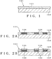
- Fig. 1 is a schematic cross-sectional view of an N-type photoconductor substrate used in the present invention.
- an N-type photoconductor substrate 101 comprises a conductive substrate 102 and an N-type photoconductor layer 103 formed on the conductive substrate 102.
- the conductive substrate 102 may comprise a metal plate, which as such is electrically conductive, such as a plate of Al, Zn, Cu, Fe, Ni, Cr, stainless steel, an alloy, or the like.
- it may comprise an electrical insulating substrate, such as glass, a plastic plate, a film, or paper, and a conductive deposit coating of indium tin oxide (ITO), tin dioxide (SnO2), a metal, or the like provided thereon or a metallic film laminated thereon.
- ITO indium tin oxide
- SnO2 tin dioxide
- Al, Zn, Stainless steel, film materials, and the like are particularly preferred. That the interface of the conductive substrate 102 and the N-type photoconductor layer 103 is electrically conductive suffices for the conductive substrate 102. Therefore, the conductive substrate 102 may be also formed of carbon or a carbon-containing conductive material.
- the N-type photoconductor layer 103 is formed of an optical memory N-type semiconductor.
- the optical memory N-type photoconductor include zinc cadmium sulfate, zinc cadmium selenide, zinc oxide, titanium oxide, and organic semiconductors. Among them, zinc oxide, titanium oxide, and the like are useful from the viewpoint of electrical properties, optical memory properties, easiness of production, profitability, and the like.
- the N-type photoconductor may be properly selected from the above materials.
- the semiconductor should satisfy such a property requirement that the electrical resistance of the optical memory area is low enough to enable the deposition of an electrodeposition material with the electrical resistance of the area, having no optical memory, being high enough to inhibit the deposition of an electrodeposition material.
- an N-type photoconductor may be preferably used which has a bright resistance of not more than 108 ⁇ cm, the difference between a dark resistance and a bright resistance being not less than 102 ⁇ cm.
- the zinc oxide for electrophotography is brought to a paste using as a binder an electrical insulating resin and the paste is homogeneously coated and dried on the conductive substrate 102 to form a coating having a thickness of several ⁇ m to 30 ⁇ m, thereby providing an N-type photoconductor substrate 101.
- Electrical insulating resins include alkyd resin, styrene/butadiene copolymer resin, and acrylic resin. In general, styrene/butadiene copolymer resin and acrylic resin are easy to handle.
- a sensitizer may be added in order to improve the spectral sensitivity of the N-type photoconductor layer 103 of zinc oxide and regulate the sensitizing wavelength.
- Sensitizers usable herein include rose bengal, bromophenol blue, and permanent blue.
- the addition of the sensitizer enables the wavelength of light used in exposure to be suitably selected in a wide range of from ultraviolet light region to visible light/near infrared region. Therefore, the N-type photoconductor substrate 101 used in the present invention has a feature that it is suitable also for output wavelengths of general-purpose lasers such as argon laser and semiconductor laser.
- the exposure of the N-type photoconductor layer 103 of the N-type photoconductor substrate 101 is carried out using a previously prepared optical drawing device or a photographic original plate (Fig. 2A).
- This exposure causes an exposed area 104 alone to develop memory type conductivity for a long period of time and serves as an electrodeposition area with the unexposed area of the N-type photoconductor layer 103 being kept in an insulating state.
- an ionic organic polymer component contained in an electrodeposition bath described below can be electrodeposited in the electrodeposition bath on the exposed area (electrodeposition area) alone, enabling an electrodeposit layer 105 to be partially formed on the N-type photoconductor substrate 101 (Fig. 2B).
- the unexposed area of the N-type photoconductor layer 103 is merely in a contaminated state without electrodeposition and, hence, can be cleaned by washing with water after the electrodeposition. After the washing with water, the electrodeposited plate is dried to provide the printing plate of the present invention.
- the printing plate 111 of the present invention thus prepared may be heated or photo-cured in order to enhance the abrasion resistance of the electrodeposit layer 105 or to increase the adhesion to the substrate for a printing plate.
- the electrodeposition may be carried out using any conventional electrodeposition device, and the principle thereof is known in the art.
- Fig. 3 shows a schematic principal diagram of an electrodeposition tank.
- the electrodeposition tank 131 contains an electrodeposition solution 132.
- the N-type photoconductor substrate 101 which has been subjected to a desired pattern-wise exposure, is used as a cathode, and an insoluble conductive material, not causing electrolytic elution, for example, Ti, Pt, or carbon electrode, is used as a counter electrode 133, i.e., a positive electrode.
- Each electrode is connected to an external direct voltage source 140.
- an ionic organic polymer component contained in the electrodeposition solution 132 is electrodeposited on the exposed area 104 of the N-type photoconductor substrate 101 to form an electrodeposit layer 105. Thereafter, the electrodeposited substrate is pulled up, washed with water, and dried to provide a printing plate 111 as shown in Fig. 2B. Since the N-type photoconductor layer 103 is a photoreceptor, all the above procedures should be carried out in a dark place or under safelight.
- the electrodeposit layer 105 is generally formed of an organic material (polymer material). It is formed by a method well known as "electrodeposition (electrocoating)." The electrodeposition is classified into cationic electrodeposition and anionic electrodeposition according to the method of electrodeposition on the surface of the main electrode. This classification is based on whether the electrodeposition material behaves as cation or anion.
- Ionic organic polymer materials usable in the electrodeposition include various organic polymer materials such as natural fats and oils, synthetic fats and oils, alkyd resins, polyester resins, acrylic resins, and epoxy resins.
- maleinized oils and polybutadiene resin are known as the ionic organic polymer material from of old, and the resultant electrodeposit layer 105 (electrodeposited material) is cured by an oxidative polymerization.
- epoxy resin organic polymer materials are mainly used alone or after modification.
- polyamide resin organic polymer materials, such as polybutadiene resin, melamine resin, and acrylic resin, and a strong electrodeposit layer 5 is formed by heat curing, photo-curing, or the like.
- photo-curing or heat curing can be facilitated by adding a curing agent, such as an amino acid or a blocked isocyanate, or introducing a polymer group or a polymerizable unsaturated group into the resin per se.
- a curing agent such as an amino acid or a blocked isocyanate
- the electrodeposited substrate in its surface comprising an oxide photoconductor is inherently hydrophilic.
- the above resins having a capability of being electrodeposited can be strongly adhered or fixed to the photoconductor. Further, in a dry state, they are receptive to an ink, facilitating the application of dampening water at the time of printing. Furthermore, since they have a high adhesion to the surface of a photoconductor, the frequency of printing failure derived from the deformation or defoliation of an electrodeposit (that is, an image area) is significantly reduced, even when a number of cyclic printing operations are carried out, providing a printing plate having high plate wear.
- a water-repellent, oil-repellent ionic organic polymer material is used as the electrodeposition materials.
- the materials having such properties include silicone resin and fluororesin, and an example of the practical use of such materials is such that these materials are electrodeposited on the surface of the structure to impart a water-repellent, oil-repellent property to the surface of the structure.
- composite plating where these resins are dispersed in a metal plating bath and co-electrodeposited simultaneously with metal electrodeposition.
- composite plating comprising a combination of a nickel plating solution with a fluororesin may be mentioned. Therefore, the printing plate of the present invention is applicable to dry lithography.
- the printing plate may be prepared quite the same manner as shown in Fig. 2.
- the printing plate preparation process is the same as the process for preparing a plate for wet lithography, and these processes are different from each other in electrodeposition material alone.
- the N-type photoconductor substrate is subjected to pattern-wise exposure, the semiconductor substrate 101 after exposure is immersed in an electrodeposition solution 132, containing an oil-repellent electrodeposition material, held in an electrodeposition tank 131 shown in Fig. 3, a counter electrode 133 is disposed, and a direct voltage is applied for electrodeposition.
- the thickness of the resultant electrodeposit coating is, for example, about 2 to 20 ⁇ m, and the electrodeposition voltage is, for example, about 40 to 100 V.
- the semiconductor substrate 101 is pulled up, washed with water, and dried to prepare a printing plate 111.
- the electrodeposit layer 105 is oil-repellent (ink-repellent), the ink does not deposit thereon.
- a naked semiconductor layer 103 which is in a dry state, is lipophilic, and the ink deposits thereon.
- the deposited ink is transferred onto a printing medium to carry out printing.
- the dry printing is opposite to the wet offset printing using dampening water and is called “waterless lithography" because no dampening water is used.
- the ink used is preferably a special ink having lower affinity for the oil-repellent area (electrodeposit layer 105).
- the dry lithography since no water is used, the dry lithography, as compared with the wet lithography, has various advantages, such as simplification of a printing machine, high-density and high-precision printing, and easy control.
- the electrodeposited oil-repellent area (oil-repellent member layer) serves as a relief plate, and the ink is deposited on the concave area. Therefore, the plate for dry lithography is exactly a deep-etch plate. In this case, the amount of the ink deposited is large. Therefore, as compared with the conventional plate for wet printing (plano-convex plate type), the amount of the ink used is larger although the density is higher.
- a plate for dry lithography which is of the same plano-convex plate type as used in the wet process, can be prepared by again subjecting the area between oil-repellent areas as a mask to exposure and electrodeposition to provide a lipophilic area (a lipophilic member layer) having a higher thickness than the oil-repellent area. Since the oil-repellent area has an electrical insulating property (this area is not electrodeposited), the re-electrodeposition on the lipophilic area can be easily carried out by subjecting the naked photoconductor to exposure on the whole area or exposure using a mask to impart selective local conductivity (a capability of being electrodeposited).
- a finely divided pigment or dye is dispersed in an anionic or cationic electrodeposition bath and co-electrodeposited together with an ionic polymer material, thereby carrying out color coating. Therefore, also in the present invention, a suitable color may be provided to the electrodeposition component in order to enhance the pattern recognition of the resultant printing plate.
- an N-type photoconductor is used, and when the N-type photoconductor is used as a main electrode for electrodeposition, electrons only are passed through the N-type photoconductor layer and the N-type photoconductor acts as a cathode. Therefore, the electrodeposition bath used should be cationic, and a cationic material is reduced and deposited on the exposed area (conductive area) of the N-type photoconductor layer.
- an electrodeposition bath of a dispersion comprising the above epoxy resin, polybutadiene resin, polyamide or other cationic resins and a colorant and electrodeposition of a metal (for example, a lipophilic metal such as Cu) using a conventional electrodeposition bath.
- a metal for example, a lipophilic metal such as Cu
- Specific examples of the cationic electrodeposition material are described in many documents, for example, Japanese Patent Publication No. 184577/1985 and Japanese Patent Laid-Open Nos. 210901/1988 and 22379/1989, and, therefore, detailed description of the cationic electrodeposition material will be omitted.
- the process for preparing a printing plate according to the present invention basically utilizes an optical memory property of a photoconductor.
- An ink-receptive component is electrodeposited on the optical memory area, and the ink-receptive component is transferred onto a hydrophilic substrate for a printing plate, thereby preparing a printing plate.
- the photoconductor as a photosensitive material used in the present invention utilizes the photoconductor substrate of the first aspect of the invention and is an optical memory N-type photoconductor which, after pattern-wise exposure, has a function of storing the exposure effect for a long period of time.
- the present invention has advantages such as high plate wear and repeated utilization of the N-type photoconductor.
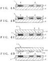
- an N-type photoconductor layer 3 in an N-type photoconductor substrate 1 is exposed using a previously prepared photo-drawing device or a photographic original plate (Fig. 4A).
- This exposure causes conductivity having an memory property to be developed in an exposed area 4 only, and the exposed area 4 serves as an electrodeposition area, while an unexposed area in the N-type photoconductor layer 3 is kept in an electrical insulating state. Therefore, an ink-receptive component contained in an electrodeposition bath described below can be electrodeposited in the electrodeposition bath on the exposed area (electrodeposition area) alone, enabling an electrodeposit layer 5 to be partially formed on the N-type photoconductor substrate 1 (Fig. 4B).
- the unexposed area of the N-type photoconductor layer 3 is merely in a contaminated state without electrodeposition and, hence, can be cleaned by washing with water after the electrodeposition.
- a substrate 12, for a printing plate at least the surface of which is hydrophilic, is brought into press contact with the ink-receptive component layer 5 on the N-type photoconductor layer 1 and then peeled off to transfer the ink-receptive component layer 5 from the N-type photoconductor substrate 1 onto the substrate 12 for a printing plate (Figs. 4C and 4D).
- an ink-receptive area 13 of a lipophilic ink-receptive component is formed on the hydrophilic substrate 12 for a printing plate, thereby preparing the printing plate 11 of the present invention.
- the selected ink-receptive component for electrodeposition in the present invention has an adhesive property at room temperature or an adhesive property when it is in a hot state.
- the substrate 12 for a printing plate may be, for example, an aluminum substrate the surface of which has been anodized to impart high friction resistance enough to withstand printing in large volumes.
- the printing plate 11 of the present invention thus prepared may be heated or photo-cured to enhance the abrasion resistance of the ink-receptive area 13 or to increase the adhesion to the substrate 12 for a printing plate, thereby improving the plate wear.
- a release layer 6 as shown in Fig. 5, which does not inhibit the electrodeposition, may be previously formed on the N-type photoconductor layer 3 of the N-type photoconductor substrate 1.
- the formation of the release layer 6 facilitates the release of the ink-receptive component layer 5 from the interface of the release layer 6, enabling the ink-receptive component layer 5 to be stably transferred onto the substrate 12 for a printing plate.
- the release layer 6 may be formed of a surfactant or silicone release agent.
- silicone generally has an electrical insulating property, it has a release effect even in a very thin coating form and does not inhibit the conductivity for electrodeposition in practical use.
- the exposed area (electrodeposition area) 4 is subjected to primary electrodeposition of a releasable material to previously form a thin electrodeposit layer 7 (Fig. 6A) and the thin electrodeposit layer 7 is then subjected to secondary electrodeposition of an ink-receptive component to form an ink-receptive component layer 5 (Fig. 6B).
- the thin electrodeposit layer 7 is transferred at the time of transfer of the ink-receptive component layer 5 onto the substrate 12 for a printing plate, thereby forming an ink-receptive area 23.
- a printing plate 21 is provided.
- the releasable material for forming the thin electrodeposit layer 7 include electrodeposition materials, for example, metals, such as Ni, Cu, Ag, and Sn, and alloys.
- the printing plate 21, as such, may be used for printing.
- the above releasable materials are inherently lipophilic and highly ink-receptive, the printing resistance can be provided to some extent.
- An oxide photoconductor such as ZnO
- ZnO is inherently chemically oxidative. Light irradiation renders the oxide semiconductor reductive. For this reason, it is known that reductive deposition (electroless plating) of a metal from a metal salt contained in a solution having a low reduction potential, such as a heavy metal salt solution, can be carried out with successful results. Therefore, it is possible to carry out selective electroless plating of a metal, such as Ni, Cu, Ag, or Sn, on light-exposed area of the oxide semiconductor, and it is also possible to form, instead of the thin deposit layer 7 by the primary electrodeposition, a thin deposit layer 7 on the exposed area 4 of the N-type photoconductor layer 3 by electroless plating.
- the other constituent features are the same as those of the first invention.
- the exposed area 4 remains conductive, enabling the N-type photoconductor substrate 1 to be repeatedly used. Therefore, a plurality of identical printing plates can be prepared by repetition of electrodeposition and transfer using an identical N-type photoconductor substrate, contributing to an increase in efficiency and a reduction in production cost.
- N-type photoconductor substrate 1 after transfer of the ink-receptive component layer 5 onto the substrate 12 for a printing plate is allowed to stand or heat-treated to erase the conductivity of the exposed area 4 and, thereafter, different pattern-wise exposure is carried out to form a new exposed area 4 which is then used for the preparation of a different printing plate. That is, a single N-type photoconductor substrate may be used a plurality of times for the preparation of various printing plates, enabling a marked reduction in production cost.
- the electrodeposition device used in the present invention may be one as shown in Fig. 3.
- An electrodeposition agent is electrodeposited according to the first aspect of the invention to form an ink-receptive component layer 105.
- the N-type photoconductor substrate 101 may be pulled up from the electrodeposition 132 and dried, and, as described above, the ink-receptive component layer 105 can be press-transferred onto the substrate 12 for a printing plate at room temperature or while heating.
- the optical memory is erased. Since the N-type photoconductor layer 103 is a photoreceptor, all the above steps should be carried out in a dark room or under safelight.
- the optical memory property (conversion to conductive state) of an photoconductor and rapid erasability (conversion to electrical insulating state) of the optical memory by heat are utilized.
- the conductivity of optical memory is developed by exposure, hot pattern drawing is carried out to erase some of the optical memory, and an electrodeposition material is electrodeposited on the area remaining conductive after the hot pattern drawing to form an electrodeposit layer, thereby preparing a printing plate.
- the electrodeposit layer is ink-receptive, ink-repellent, or dampening water-receptive depending upon the electrodeposition material constituting the electrodeposit layer.
- the photoconductor as a photosensitive material used in the present invention is an N-type photoconductor having an optical memory property such that the conductivity is developed by exposure and the exposure effect is stored for a long period of time.
- the present invention uses the photoconductor substrate of the first aspect of the invention, that is, is a modified process of the present invention.
- a certain N-type photoconductor has an optical memory property such that the light irradiation effect (exposure effect) can be stored for a certain period of time.
- This optical memory property is not permanent but kept for a period of time which varies depending upon the material used. It disappears after the given period of time, and the insulating property is recovered. The time taken for the recovery can be markedly shortened by suitable heating.
- the present invention is based on effective use of the erasability of the optical memory by heat.
- an object of the third aspect of the invention is to provide a process for simply producing a printing plate which can provide a print having a high quality and a high plate wear.
- the process for producing a printing plate according to the third aspect comprises the steps of: providing an N-type photoconductor layer having an optical memory property on the surface of a substrate having an electrical conductivity at least in its surface to form an N-type photoconductor substrate; exposing the whole surface or a necessary region of the N-type photoconductor layer to render exposed areas electrically conductive; heating the exposed areas by hot pattern drawing to erase the conductivity of the heated areas; immersing the N-type photoconductor substrate in an electrodeposition bath to electrodeposit an electrodeposition material on the remaining conductive areas alone to form an electrodeposit layer; and washing and drying the electrodeposited substrate to prepare a printing plate.
- Another process for preparing a printing plate according to the present invention comprises the steps of: providing an N-type photoconductor layer having an optical memory property on the surface of a substrate having an electrical conductivity at least in its surface to form an N-type photoconductor substrate; exposing the whole surface or a necessary region of the N-type photoconductor layer to render exposed areas electrically conductive; heating the exposed areas by hot pattern drawing to erase the conductivity of the heated areas; immersing the N-type photoconductor substrate in an electrodeposition bath to electrodeposit a light-screening and/or electrical insulating first electrodeposit layer on the remaining conductive areas alone to form a first electrodeposit layer; washing the electrodeposited substrate; exposing the N-type photoconductor substrate to again render exposed areas electrically conductive; immersing the N-type photoconductor substrate in an electrodeposition bath to electrodeposit a second electrodeposition material on only areas with the first deposit layer having not been formed, thereby forming a second electrodeposit layer; and washing and drying the electrodeposited substrate to
- the N-type photoconductor layer in its entirety or necessary region of the N-type photoconductor substrate is rendered conductive by exposure, the exposed areas is heated by hot pattern drawing to erase the conductivity of the heated areas, and an electrodeposition material is electrodeposited on the remaining conductive areas to prepare a printing plate.
- Any of printing plates for wet printing and dry printing may be prepared by the same process through the selection of properties (repellency or receptivity to ink and receptivity to dampening water) of the N-type photoconductor layer and the electrodeposition material.
- a light-screening and/or electrical insulating first electrodeposit layer is electrodeposited on the remaining conductive areas to form a first electrodeposit layer, the N-type photoconductor substrate is again exposed to again render exposed areas electrically conductive, and a second electrodeposition material is electrodeposited on only areas with the first deposit layer having not been formed (when the first electrodeposition material has an electrical insulating property, such areas correspond to the exposed areas, while when the first electrodeposition material has an electrical insulating property alone, the first electrodeposit layer serves as an insulating mask), thereby forming a second electrodeposit layer.
- a printing plate is prepared.
- a plate for dry printing can be provided by rendering any one of the first electrodeposit layer and the second electrodeposit layer ink-receptive with the other being rendered ink-repellent.
- a plate for wet printing can be provided by rendering any one of the first electrodeposit layer and the second electrodeposit layer ink-receptive with the other being rendered hydrophilic.
- any of a printing plate for wet printing and a printing plate for dry printing which can provide a high-quality print with a high plate wear, may be prepared in the same process. Further, it is also possible to use a thermal process using a laser beam, which process can cope with digital data.
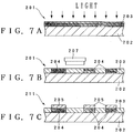
- an image pattern is formed using a suitable heat source 207 on the surface of the conductive N-type photoconductor layer 203 (Fig. 7B). This erases the conductivity at the heated areas, causing the insulating property to be locally returned with the other areas (unheated areas) being left as remaining conductive areas 204.
- the N-type photoconductor substrate 201 is subjected to electrodeposition in an electrodeposition bath, whereby the electrodeposition material 205 can be deposited on the remaining conductive areas only. Consequently, an electrodeposit layer 205 is partially formed on the N-type photoconductor substrate 201 (Fig. 7C). On the other hand, electrodeposition does not occur on the areas which has been locally returned to an electrical insulating state.
- the printing plate 211 of the present invention thus prepared may be heated or photo-cured to enhance the abrasion resistance of the electrodeposit layer 205 to increase the adhesion to the N-type photoconductor layer 203, thereby improving the plate wear.
- the electrodeposition material is generally receptive to an ink
- the electrodeposit layer 205 can be easily inked at the time of printing.
- the surface of the N-type photoconductor layer is hydrophilic and, hence, has good receptivity to dampening water. Therefore, the printing plate 211 can be effectively utilized for wet lithography.
- the electrodeposit layer 205 becomes ink-repellent, so that no ink is deposited on the layer 205 with the ink being deposited on the dried surface of the N-type photoconductor layer. Therefore, in this case, the resultant printing plate can be used for dry lithography wherein no dampening water is used.
- An example of electrodeposition of a water-repellent, oil-repellent resin is to impart a water-repellent, oil-repellent property to the surface of the structure.
- a finely divided pigment or dye may be dispersed in the ionic electrodeposition bath and co-deposited together with the ionic polymer material at the time of electrodeposition, thereby providing a colored deposit.
- the pattern recognition of the printing plate can be improved by coloring of the electrodeposit layer 205, or fillers can be used to improve the properties of the electrodeposit layer 205.
- an electrodeposition solution with polytetrafluoroethylene (PTFE: teflon) being dispersed therein may be used to form an electrodeposit layer 205 having increased ink repellency, thereby improving the suitability of the printing plate 211 for dry printing.
- PTFE polytetrafluoroethylene
- Specific examples of such electrodeposition solution include a combined electrodeposition solution in the form of a dispersion of PTFE in a nickel ion solution.
- hot pattern drawing for thermally erasing the memory-type conductivity developed in the N-type semiconductor layer 203 may be carried out by various methods such as the simplest method wherein hot drawing is carried out with a suitable hot pen, a method wherein recording is carried out by means of a thermal recording head provided with a heating element, a method wherein a gas laser beam or a semiconductor laser beam is condensed to carry out scanning recording in a heat mode, and a method wherein a pattern permeable to hot rays is previously prepared, brought into close contact with the semiconductor layer, and subjected to batch exposure to infrared light. All of these thermal recording means are known in the art, and, therefore, detailed description thereof will be omitted.
- an N-type photoconductor substrate 201 is subjected to homogeneous exposure and hot pattern drawing to form an ink-receptive or ink-repellent electrodeposit layer, and the hydrophilicity of the N-type photoconductor layer 203 and the ink deposition thereof in a dried state are utilized to prepare a plate for wet or dry printing.
- the printing plate prepared by the above printing plate preparation process is a printing plate utilizing the difference in properties between the electrodeposit layer and the N-type photoconductor layer.
- the property difference can be further made large to prepare a printing plate having further improved suitability for printing.
- a printing plate for dry lithography in order to further enhance the ink repellency of the ink-repellent electrodeposit layer, it is difficult to select a proper material.
- the formation of an electrodeposit layer having higher receptivity to an ink than the N-type photoconductor layer is relatively easy.
- an N-type photoconductor layer 203 of an N-type photoconductor substrate 201 is homogeneously exposed in the same manner as in the above printing plate preparation process (Fig. 8A).
- an image pattern is drawn on the conductive area of the N-type photoconductor layer 203 by means of a suitable heat source 207 (Fig. 8B).
- the N-type photoconductor substrate 201 is subjected to electrodeposition in an electrodeposition tank to electrodeposit a light-screening and/or electrical insulating first electrodeposition material, thereby forming a first electrodeposit layer 225 (Fig. 8C). Therefore, the first electrodeposit layer 225 thus formed has a light-screening and/or electrical insulating property.
- the N-type photoconductor substrate 201 is heated or allowed to stand for a long period of time to erase the remaining conductive area 204 of the N-type photoconductor layer 203.
- the whole surface of the N-type photoconductor substrate 201 is subjected to homogeneous exposure using the first electrodeposit layer 225 as a light-screening mask (Fig. 8D).
- the first electrodeposit layer 225 has a light-screening property
- the N-type photoconductor layer 203 in only its areas where no first electrodeposit layer 225 has been formed is exposed to again develop the conductivity (Fig. 8D showing this embodiment).
- the conductivity is again developed on the whole surface of the N-type photoconductor layer 203 (not shown).
- the N-type photoconductor substrate 201 is subjected to electrodeposition in an electrodeposition bath to electrodeposit a second electrodeposition material, having properties different from the first electrodeposition material on the exposed area 204' (conductive area) only (when the first electrodeposit layer 225 has a light-screening property) to form a second electrodeposit layer 226, thereby preparing a printing plate 221 (Fig. 8E).
- the conductivity is developed also in the N-type photoconductor layer 203 underlying the first electrodeposit layer 225.
- the first electrodeposit layer 225 serves as an insulating mask at the time of electrodeposition of the second electrodeposition material, so that the second electrodeposit layer 226 is formed in only the areas where no first electrodeposit layer has been formed. Therefore, the resultant printing plate 221 is the same as in the above case (when the first electrodeposit layer 225 has a light-screening property).
- the printing plate 221 prepared by combining the first electrodeposition material with the second electrodeposition material in such a manner that the second electrodeposit layer 226 is rendered ink-repellent when the first electrodeposit layer 225 is ink-receptive, while the second electrodeposit layer 226 is rendered ink-receptive when the first electrodeposit layer 225 is ink-repellent, has a greater difference between the ink repellency and the ink receptivity, so that the suitability of the printing plate 221 for dry printing is superior.
- the lipophilicity of the N-type photoconductor 203 is generally lower than that of the electrodeposit layer
- the addition of an acrylic resin or an epoxy resin to the electrodeposit layer can improve the lipophilicity of the electrodeposit layer, which makes it possible to easily prepare a plate, for dry printing, having a large difference between the ink receptivity and the ink repellency and better suitability for dry printing.
- the other constituent features are the same as those of the first invention.
- a paste of an N-type photoconductor having the following composition was coated on a 0.15 mm-thick aluminum substrate having a specular surface, and the resultant coating was dried to form a 10 ⁇ m-thick coating, thereby preparing an N-type photoconductor substrate.
- the N-type photoconductor substrate was allowed to stand in a dark room overnight to erase the optical memory effect, and previously prepared 175 line/in. halftone plate and negative photographic film containing a letter were brought into close contact with the surface of the N-type photoconductor substrate, and the resultant laminate was exposed to tungsten light. Thereafter, the substrate was immersed in the following electrodeposition bath to electrodeposit an ink-receptive component.
- the electrodeposition conditions were as follows.
- Acrylic resin 50 parts Ethyl cellosolve 25 parts Isopropyl alcohol 3 parts Acetic acid 1.5 parts Phthalocyanine blue pigment 3 parts Water 800 parts
- acrylic resin, ethyl cellosolve, and the pigment were mixed together.
- the resultant mixture was milled in a ball mill until the pigment particles became fine.
- the remaining components were added thereto, and the mixture was stirred to prepare the above composition.
- Main electrode cathode Counter electrode: titanium Distance between electrodes: 5 to 10 cm Bath temp.: 25°C Applied voltage: 60 to 80 V Thickness of electrodeposit coating: about 3 ⁇ m Drying after electrodeposition: washing with water followed by air blow to blow off free water Heat treatment: 100 to 130°C for 10 to 20 min The photoconductor printing plate was applied to the following wet offset printing.
- a conventional simple offset sheet-fed press (a printing machine manufactured by AB Dick Co., Ltd. for the present example), as such, was used without any modification.
- a conventional printing method a conventional offset ink and dampening water were used, the above photoconductor printing plate was set in a printing roll and lightly wiped with an etchant to regulate the receptivity to dampening water, a necessary amount of dampening water was applied, inking was carried out, and paper was fed to initiate printing.
- the prints thus obtained were good, and the quality thereof was comparable to that of prints obtained by a PS plate.
- the plate wear was not less then several tens of thousands of sheets.
- the printing plate of the present invention had a quality equal to the PS plate.
- Example A2 a 0.2 mm-thick polyester film with a deposit coating of aluminum formed on one side thereof was used as a film substrate instead of the aluminum substrate of Example A1.
- the method of forming an photoconductor layer, the composition of an electrodeposition bath, conditions for preparation of a printing plate by electrodeposition were the same as those of Example A1, except that a flat bed type argon laser drawing devise was used for pattern-wise exposure to attempt a digital direct plate preparation of a 175 line halftone plate.
- the heat treatment after a series of steps of electrodeposition, washing with water and drying, was not carried out, and, after washing with water and air blowing, the plate was allowed to stand in a room or alternatively dried by air of several tens of °C to complete the preparation of a printing plate.
- Example A1 In a printing operation, the quality of the prints was similar to that of Example A1.
- Example A1 and Example A2 a commercially available ultraviolet curing cationic electrodeposition material was used as an ionic ink-receptive organic polymeric material.
- the ultraviolet curing electrodeposition material used was cationic Elecoat UC 500 (trade name), manufactured by Shimidzu Co., Ltd., which was composed mainly of a polymer having a photo-curable acryloyl group. Electrodeposition was carried out according to the following procedure.
- Electrodeposition time about 20 sec Drying and curing conditions Redrying: about 75°C Curing (Hg lamp used): not less than 800 mj/cm2
- photo-curing after the electrodeposition provided printing plates having quality and printing performance equivalent to those in Example A1 and Example A2. It was confirmed that these printing plates could be effectively used in wet offset printing.
- Example A4 a dry offset (a waterless) printing plate was prepared, and printing was actually carried out according to the following procedure.
- the photoconductor substrates used were the same as those in Example A1 and Example A2. Pattern-wise exposure was carried out in the same manner as in Example A1 and Example A2.
- a dispersion prepared by mixing and dispersing an ionic fluoropolymer and an atomized (average particle diameter: 0.2 ⁇ m) teflon (tetrafluoroethane (PTFE)) in each other was used as the electrodeposition material.
- the electrodeposition material containing an ionic fluoropolymer exists as a commercially available product called "Elecoat Nicelon ((trade name) manufactured by Shimidzu Co., Ltd.).
- the structure of this material is mainly such that a side chain having a perfluoro group is attached as a pendant group to an acrylic skeleton.
- This material is water-repellent and oil-repellent.
- it has a feature that it can satisfactorily disperse PTFE having better water repellency and oil repellency and homogeneously co-precipitate PTFE in an electrodeposit coating, resulting in further improved water repellency and oil repellency.
- an electrocoating prepared by incorporating PTFE in an amount of 25% (weight ratio on a solid basis) into Elecoat Nicelon was used as the water-repellent, oil-repellent electrodeposition material.
- Electrodeposition was carried out under the same conditions as that in Example A3 to form an about 4 ⁇ m-thick electrodeposit coating.
- Heat treatment after a series of steps of electrodeposition-washing with water-drying increases the concentration of PTFE particles around the surface of the electrodeposit coating, enhancing the oil-repellent effect. For this reason, heat treatment was carried out at 180 to 200°C for about 10 min in the case of the aluminum substrate and at 120°C for 10 min in the case of the polyester film substrate to prepare printing plates.
- Dry offset printing was carried out according to the following procedure.
- the printing machine used in the previous examples was used also in this example.
- a printing plate was mounted on a plate cylinder, and a blanket cylinder and an impression cylinder were adjusted. Thereafter, a conventional special printing ink for a silicone plate (a silicone plate being commonly used for dry printing) was placed in an ink duct and fed to the printing plate through an ink roller without use of dampening water.
- a major difference between the special ink for dry printing used herein and an ink for wet printing is that the special ink for dry printing has very high tackiness (i.e., is sensuously hard) and, unlike the ink for wet printing, does not have sticky high enough to cause thread-forming.
- the ink was not deposited on the oil-repellent electrodeposit but deposited only on the surface of the exposed photoconductor layer.
- the deposited ink was transferred onto the blanket according to the printing mechanism and again transferred onto paper being passed through the blanket cylinder to carry out printing.
- the printing machine could be operated with good results.
- This system is more exactly a dry deep-etch plate offset printing method wherein an ink is fed into a dent or concave between protruded oil-repellent material layers. For this reason, the amount of the ink used was large, and high-density prints could be obtained as in the case of dry printing using the conventional silicone plate.
- the plate wear was not less than 100000 sheets for the aluminum plate and about 20000 sheets for the polyester plate.
- the surface of the printing plate was sufficiently exposed to ultraviolet light (intense tungsten light may also be usable), and electrodeposition was carried out using the electrocoating of Example A3 to form an ink-receptive layer between the oil-repellent layers.
- the already formed oil-repellent layer has an electrical insulating property and, hence, serves as an electro deposition mask to prevent an electrodeposit from being deposited thereon.
- the ink-receptive layer was electrodeposited between the oil-repellent layers to a thickness larger by 2 to 3 ⁇ m than the thickness of the oil-repellent layer.
- the so-called "plano-convex plate" was obtained wherein the ink-receptive layer was in a protruded state.
- plano-convex plate type dry printing plate had advantages including that the provision of the ink-receptive layer facilitated the deposition of the ink enabling easily inking, the amount of the ink used is smaller than that in the case of the deep-etch plate and the transfer onto the blanket and the paper is easier.
- a 0.2 mm-thick polyester film with a deposit coating of aluminum formed on one side thereof was used as a film substrate.
- a paste of an N-type photoconductor having the following composition was coated thereon, and the resultant coating was dried to form a 10 ⁇ m-thick photoconductor layer.
- Zinc oxide SAZEX 2000, manufactured by Sakai Chemical Co., Ltd.
- Titanium oxide rutile type
- BM-S Polyvinyl butyral
- the N-type photoconductor substrate was allowed to stand in a dark room overnight to erase the optical memory effect, and previously prepared 175 line/in. halftone plate and negative photographic film containing a letter were brought into close contact with the surface of the N-type photoconductor substrate, and the resultant laminate was exposed to light from a high pressure mercury lamp. Thereafter, the substrate was then immersed in the electrodeposition bath of Example A3 to electrodeposit an ink-receptive component. The electrodeposition was carried out in the same manner as in Example A3.
- photo-curing after the electrodeposition provided a printing plate having a quality and a plate wear equivalent to those in Example A3. It was confirmed that the printing plate could be effectively used in wet offset printing.
- a comparison of printing plates using an photoconductor having an optical memory property according to the present invention and a process for producing the same with the conventional PS plates, printing plates by electrophotography, and silver salt printing plates, and the like reveals that, in general, the low cost and easy processing are comparable to those in the printing plates prepared by electrophotography, the quality (the quality of the printed image, plate wear, and the like) is comparable to that of the PS plates and the sensitivity is comparable to that attained in the electrophotography and the silver salt process (the optical drawing method or the like being usable), that is, that the printing plate of the present invention is a versatile printing plate.
- the process for preparing a printing method and the printing plate according to the present invention have, unlike the conventional plate preparation processes and printing plates, versatility, enabling the use in various printing processes, such that printing can be carried out in the conventional wet printing using dampening water by the conventional method, a printing plate for dry printing not using dampening water can be easily prepared in the same manner by using an oil-repellent electrodeposition material and offset printing and direct printing (particularly in dry process) are possible.
- the use of the printing plate and the plate preparation process according to the present invention enables printing which copes with a wider range of prints and offers various effects including that the amount of ink consumed can be reduced, high-density printing is possible and high added values can be provided such as the provision of cost-effective and high-quality prints in various fields.
- a paste of an N-type photoconductor having the following composition was coated on a 0.15 mm-thick aluminum substrate having a specular surface, and the resultant coating was dried to form a 10 ⁇ m-thick coating. Further, a dilute solution of a silicone release agent was lightly coated at such a coverage as will not inhibit the conductivity to prepare an N-type photoconductor substrate.
- Acrylic resin 50 parts Ethyl cellosolve 25 parts Isopropyl alcohol 3 parts Acetic acid 1.5 parts Phthalocyanine blue pigment 3 parts Water 800 parts
- acrylic resin, ethyl cellosolve, and the pigment were mixed together.
- the resultant mixture was milled in a ball mill until the pigment particles became fine (not more than 0.2 ⁇ m).
- the remaining components were added thereto, and the mixture was stirred to prepare the above composition.
- Main electrode cathode Counter electrode: platinum plate Applied voltage: increased from an initial voltage of 20 V gradually to 80 V according to an increase in an electrodeposit coating. Thickness of electrodeposit coating: about 3 ⁇ m Drying after electrodeposition: washing with water followed by air blow to blow off free water Then, a 0.2 mm-thick aluminum substrate, of which the surface has been rendered hydrophilic by anodization, was prepared as a substrate for a printing plate. The aluminum substrate was put on top of the N-type photoconductor substrate so that the anodized surface of the aluminum substrate faced the electrodeposited surface of the N-type photoconductor substrate.
- the laminate was pressed, and both the substrates were separated from each other to transfer the electrodeposited ink-receptive component of the N-type photoconductor substrate onto the aluminum substrate. All the above steps of exposure, electrodeposition, and transfer were carried out in a dark room.
- the aluminum substrate was heat-treated at 150°C for 10 to 20 min to improve the adhesion of the transferred ink-receptive portion and to impart the plate wear, thereby preparing the printing plate of the present invention.
- Printing was carried out by a sheet-fed offset press using the printing plate.
- the pretreatment of the printing plate at the time of printing was carried out in the same manner as used in the conventional PS plate.
- the plate wear of the printing plate according to the present invention was about 100000 sheets, and the quality of the prints was good.
- the above N-type photoconductor substrate could be repeatedly used for electrodeposition and transfer operations to prepare 10 or more identical printing plates.
- N-type photoconductor substrate was prepared in the same manner as in Example B1, except that no silicone release agent was coated. The substrate was then exposed in the same manner as in Example B1.
- the N-type photoconductor substrate was immersed in the following electrodeposition bath to carry out primary electrodeposition of Cu on the exposed area.
- the primary electrodeposition was carried out under the following conditions.
- Example B1 pH of bath for primary electrodeposition of Cu: 8.8 Temp. of bath for primary electrodeposition of Cu: 55°C Electrodeposition rate (5 A/dm2): 1.0 ⁇ m/min Secondary electrodeposition of the ink-receptive component on Cu was carried out in the same manner as in Example B1, and the ink-receptive component was transferred onto the aluminum substrate in the same manner as in Example B1 to prepare the printing plate of the present invention.
- the ink-receptive portion of the printing plate had a copper color because Cu had been transferred together with the ink-receptive component.
- the printing plate was heat-treated in the same manner as in Example B1, and the surface of the printing plate was washed with a dilute ferric chloride (FeCl3) solution to remove Cu present on the surface of the ink-receptive portion.
- Printing was carried out using this printing plate in the same manner as in Example B1.
- the plate wear was about 100000, and the quality of the prints was good.
- the plate wear was about several thousands to ten thousand sheets, and Cu was partially peeled off to cause unevenness of printing.
- N-type photoconductor substrate was prepared in the same manner as in Example B1, except that a flexible substrate of a 0.2 mm-thick polyester film with an aluminum foil bonded thereto was used instead of the aluminum substrate of Example B1.
- the N-type photoconductor substrate was wound around a drum type argon laser drawing device (an exposing device) and exposed using a 200 line/in. halftone plate, and electrodeposition and transfer were carried out in the same manner as in Example B1 to prepare a printing plate.
- the printing plate was heat-treated in the same manner as in Example B1.
- Printing was carried out in the same manner as in Example B1, except that the above heat-treated printing plate was used. As a result, the plate wear of the printing plate was about 100000, and the quality of the prints was good.
- the N-type photoconductor substrate after transfer was heat-treated at 80 to 110°C for 10 to 20 min to erase the optical memory (electrical conductivity at the exposed area), cooled at room temperature, and again subjected to optical drawing exposure using other image data, electrodeposition, and transfer, thereby preparing a printing plate.
- the above N-type photoconductor substrate could be repeatedly used for electrodeposition and transfer operations to prepare 10 or more identical printing plates.
- N-type photoconductor substrate was prepared in the same manner as in Example B3, and optical drawing exposure was carried out. Then, the N-type photoconductor was immersed in an electrodeposition bath to electrodeposit the ink-receptive component.
- the electrodeposition bath used was prepared as follows. At the outset, N,N-dimetylaminoethyl acrylate: 115 parts, 2-hydroxyethyl methacrylate: 150 parts, n-butyl acrylate: 400 parts, methyl methacrylate: 150 parts, n-butyl methacrylate: 185 parts, and azobisisobutyronitrile: 50 parts were mixed together, and a reaction was allowed to proceed to prepare as a stock solution (solid content: about 60%) a solution of an adhesive electrodeposition material dissolved in ethyl cellosolve.
- Main electrode cathode Counter electrode: platinum plate Applied voltage: 80 V (for 60 sec) Drying after electrodeposition: washing with water followed by air blow to blow off free water
- the surface of the ink-receptive component electrodeposited on the N-type photoconductor substrate was highly adhesive, and when the N-type photoconductor substrate was pressed against the anodized aluminum substrate as the substrate for a printing plate, the ink-receptive component was easily peeled and transferred onto the side of the anodised aluminum substrate.
- the printing plate thus prepared was heat-treated at 130°C for 10 min, and printing was carried out using this printing plate in the same manner as in Example B1. As a result, the plate wear was about 100000, and the quality of the prints was good.
- a paste of an N-type photoconductor having the following composition was coated on a flexible substrate of a 0.2 mm-thick polyester film with an aluminum foil adhered thereto, and the resultant coating was dried to form a 10 ⁇ m-thick coating. Further, a dilute solution of a silicone release agent was lightly coated in such an amount as will not sacrifice the electrical conductivity, thereby preparing an N-type photoconductor substrate.
- Titanium oxide 20 g Polyvinyl butyral (BM-S, manufactured by Sekisui Chemical Co., Ltd.) 5 g Toluene 40 ml
- a printing plate was prepared in the same manner as described just above, except that a paper substrate was used as the substrate for a printing plate instead of the anodized aluminum substrate and the heat treatment at 130°C for 10 min was omitted.
- the paper substrate used was such that an agent, for imparting a hydrophilic property, comprising a titanium white pigment as a main component and a hydrophilic polymer material (such as PVA) as a binder was coated on the surface of water-resistant paper (thickness 0.3 mm) to render the whole surface of the paper receptive to dampening water.
- Printing was carried out using this printing plate in the same manner as in Example 1, and the quality of the prints was good. Due to the omission of the heat treatment, the use of the paper substrate, and other factors, the plate wear was about several thousand to ten thousand sheets.
- N-type photoconductor substrate could be repeatedly used for electrodeposition and transfer operations to prepare 10 or more identical printing plates.
- the present invention enables a printing plate to be prepared by a very simple process by taking advantage of an N-type photoconductor substrate and the persistence of the exposure effect or memory property thereof. Further, the transfer of an ink-receptive component onto the surface of a hydrophilic substrate as a substrate for a printing plate enables the transferred ink-receptive component to be used as an ink-receptive component of the printing plate. Since the ink-receptive portion can be formed homogeneously with high resolution and high fineness, the resultant printing plate has excellent plate wear and can provide high-quality prints.
- an identical N-type photoconductor substrate can be repeatedly used for the production of a plurality of identical printing plates. Furthermore, since the optical memory property of the N-type photoconductor layer can be easily erased, the identical N-type photoconductor substrate can be repeatedly used for exposure and electrodeposition and transfer, which enables a plurality of different types of printing plates to be prepared from an identical N-type photoconductor substrate. Furthermore, digital images and numerical design data subjected to image processing can be utilized in an optical drawing device, enabling optical drawing to become possible without use of any photographic original plate. This further simplifies the process, resulting in a marked reduction in production cost.
- a deposit coating of aluminum was formed on one side of a 0.2 mm-thick polyester film, and the aluminum-deposited film was used as a substrate.
- a paste of an N-type photoconductor having the following composition was coated thereon, and the resultant coating was dried to form a 20 ⁇ m-thick dried coating, thereby preparing an N-type photoconductor substrate. Since the preparation of the N-type photoconductor substrate was carried out in a bright room, the whole surface of the N-type photoconductor layer became electrically conductive.
- Acrylic resin 50 parts Ethyl cellosolve 25 parts Isopropyl alcohol 3 parts Acetic acid 1.5 parts Water 800 parts Phthalocyanine blue (pigment) 3 parts
- acrylic resin, ethyl cellosolve, and the pigment were mixed together.
- the resultant mixture was milled in a ball mill until the pigment particles became fine (not more than 0.2 ⁇ m).
- the remaining components were added thereto, and the mixture was stirred to prepare the above composition.
- Main electrode N-type optical semiconductor substrate
- cathode Counter electrode titanium plate Distance between electrodes: 5 to 10 cm
- Applied voltage 60 V
- Bath temp. 25°C
- Thickness of electrodeposit coating about 3 ⁇ m
- Drying after electrodeposition washing with water followed by air blow to blow off free water
- the resultant printing plate was used to carry out printing by means of a simple offset sheet-fed press (manufactured by AB Dick Co., Ltd.).
- the ink, dampening water, and etchant used were commercially available products.
- the printing plate was mounted on a plate cylinder, and the surface thereof was lightly treated with the etchant.
- the amount of necessary dampening water was regulated, and inking and feed of paper were carried out for printing.
- the prints obtained using the printing plate according to the present invention had a good quality which was comparable to the quality of prints obtained using a PS plate.
- N-type photoconductor substrate was prepared in a bright place in the same manner as in Example C1.
- N-type semiconductor substrate Thereafter, two types of digital thermal recording were carried out on the N-type semiconductor substrate.
- One of them was thermal recording using a thermal head for conventional thermal recording, and the other was scanning thermal recording using 500 mmW large output semiconductor laser (870 nm).
- a 1 ⁇ m-thick black coating layer (containing carbon) was provided on one side of a 175 ⁇ m-thick transparent polyester film, the transparent polyester film and the N-type photoconductor substrate were brought into close contact with each other so that the black coating layer faced N-type photoconductor layer.
- Electrodeposition was carried out under the same conditions as those of Example C1 to prepare a printing plate for wet lithography.
- N-type photoconductor substrate was prepared in a bright place in the same manner as in Example C1.
- the N-type photoconductor substrate was immersed in an electrodeposition bath to electrodeposit an ink-repellent component on the remaining conductive portion, thereby forming an electrodeposit layer.
- the composition of the electrodeposition bath used was the same as that in Example C1, except that the following oil-repellent resin component was used instead of the electrodeposition resin component in Example C1. Further, the electrodeposition conditions were the same as those used in Example C1.
- the ionic fluoropolymer has a structure such that a side chain having a perfluoro group is attached to an acrylic skeleton. This material, as such, is water-repellent and oil-repellent. In addition, it has a feature that it can satisfactorily disperse PTFE having better water repellency and oil repellency and homogeneously co-precipitate PTFE in an electrodeposit coating.
- the heat treatment was carried out at 120°C for 10 min to prepare a printing plate for dry lithography.
- the resultant printing plate was mounted on a plate cylinder of a simple offset sheet-fed press (manufactured by AB Dick Co., Ltd.), and a blanket cylinder and an impression cylinder were adjusted. Thereafter, a conventional special printing ink for a silicone plate was placed in an ink duct and fed to the printing plate through an ink roller without use of dampening water, and printing was then carried out on sheets.
- the ink was not deposited on the oil-repellent electrodeposit but deposited only on the surface of the exposed surface of the N-type photoconductor layer.
- the deposited ink was transferred onto the blanket according to the printing mechanism and again transferred onto paper being passed through the blanket cylinder to carry out printing.
- the plate wear was about 20000 sheets.
- N-type photoconductor substrate was prepared in a bright place in the same manner as in Example C1.
- a first electrodeposit layer (thickness 2 ⁇ m) was formed by electrodeposition of an ink-repellent component on the remaining conductive portions in an electrodeposition bath in the same manner as in Example C3.
- the composition of the electrodeposition bath used was the same as that in Example C3.
- the N-type photoconductor substrate was then allowed to stand in a bright place for several hours (or alternatively may be exposed to light from a 1 kW mercury lamp for 10 sec) to again expose the N-type photoconductor substrate, thereby rendering the whole surface of the N-type photoconductor layer (including a region where the first electrodeposit layer is formed) electrically conductive. Thereafter, an ink-receptive component was electrodeposited on the conductive portion using same electrodeposition bath and electrodeposition conditions as in Example C1, thereby forming a second electrodeposit layer (thickness 3 ⁇ m).
- the second electrodeposit layer is not formed on the first electrodeposit layer. Thereafter, washing with water and drying followed by heat treatment at 120°C for 10 min were carried out to prepare a plate A for dry printing.
- an N-type photoconductor substrate was prepared in a bright place in the same manner as in Example C1, and digital thermal recording (negative mode) was carried out by means of a thermal head on an N-type photoconductor substrate in the same manner as in Example C2.
- an ink-receptive component was electrodeposited on the remaining conductive portions using the same electrodeposition bath (except that 15 parts of carbon black was used instead of 3 parts of phthalocyanine as the color component) and electrodeposition conditions as in Example C1 to form a first electrodeposit layer (thickness 3 ⁇ m).
- the first electrodeposit layer contains carbon black. Therefore, although the electrical insulating property thereof is unsatisfactory as compared with that of the first electrodeposit layer in the printing plate A, it has a light screening property.
- the N-type photoconductor substrate was exposed for a short period of time (exposed to light from a 1 kW mercury lamp for 10 sec).
- the first electrodeposit layer served as a light screening mask, and the N-type photoconductor layer in its region where no first electrodeposit layer had been formed was again rendered electrically conductive.
- an ink-repellent component was electrodeposited on the conductive areas in an electrodeposition bath in the same manner as in Example C3, thereby forming a second electrodeposit layer (thickness 2 ⁇ m).
- the composition of the electrodeposition bath used was that of the electrodeposition bath of Example C3.
- washing with water and drying were curried out followed by heat treatment at 120°C for 10 min, thereby preparing a plate B for dry printing.
- the printing plate of Example C3 is a deep-etch plate consisting of an N-type semiconductor layer and an oil-repellent electrodeposit layer, and inking is carried out in the concave areas (N-type semiconductor layer), so that the amount of the ink used is large although high-density printing is possible.
- the printing plates A and B of Example C4 are of plano-convex type (the same type as the conventional wet lithography) wherein the ink-receptive area is 1 ⁇ m higher than the oil-receptive area, so that the amount of the ink used is substantially the same as that in the case of wet lithography, enabling the amount of the ink used to be reduced as compared with the conventional dry lithography.
- the printing plates A and B of Example C4 are of plano-convex type, the deposition of the ink is good enough to facilitate inking. Further, as opposed to wet printing, emulsification of ink by dampening water does not occur. Therefore, high-density printing is possible even when the amount of the ink used may be smaller than that used in the wet printing. In addition, sharper printed images can be provided.
- the second electrodeposit layer as the ink-receptive area of the printing plate A in Example 4 and the first electrodeposit layer as the ink-receptive area of the printing plate B in Example C4 have a higher lipophilic property than the N-type semiconductor layer as the ink-receptive area of Example C3, so that inking is possible even when an ink having higher tackiness than a special ink for dry printing is used. For this reason, it is expected that in the preparation of an ink which is less susceptible to scumming or tinting of the print and failure of inking, a design having a higher degree of freedom is possible, which in turn makes it possible to prepare an ink which is easy to use.
- a paste of an N-type photoconductor having the following composition was coated on a 0.15 mm-thick aluminum substrate having a specular surface, and the resultant coating was dried to form a 20 ⁇ m-thick coating, thereby preparing an N-type photoconductor substrate.
- Zinc oxide (SAZEX 2000, manufactured by Sakai Chemical Co., Ltd.) 4 g Titanium oxide (rutile type) 16 g Dye having absorption in near infrared region (Kayasorb CY-10, manufactured by Nippon Kayaku Co., Ltd.) 0.1 g Polyvinyl butyral (BM-S, manufactured by Sekisui Chemical Co., Ltd.) 5 g Toluene 50 ml
- Example C1 After exposure with a high pressure mercury lamp, scanning thermal recording was carried out using a semiconductor laser (780 nm) having a large output of 500 mW.
- the recording mode was negative, the recording density was 2500 dpi, and output images were letters, including kanji (Chinese characters), and symbols of 2 points, 4 points, and 6 points.
- electrodeposition was carried out under the same conditions as those of Example C1 to prepare a printing plate for wet lithography. Offset printing was carried out using the resultant printing plate in the same manner as in Example C1. As a result, it was confirmed that the quality of prints obtained using the printing plate of the present invention was good and corresponded to 2500 dpi.
- the utilization of an N-type semiconductor substrate having an optical memory property, the persistence of the exposure effect, and the formation of a pattern latent image by erase upon heating can highly simplify the process, enabling shortening and simplification of the plate preparation process and an improvement in reliability of the operation.
- plates for wet or dry printing which provide high-quality prints with high plate wear, can be freely prepared by an identical process through the selection of an electrodeposition material, which enables the preparation of printing plates having versatility high enough to be applicable to various printing processes.
- thermal plate preparation since thermal plate preparation is possible, plate preparation utilizing laser or precise thermal head is applicable to the field of high-quality printing, so that the formation of a pattern by using the conventional thermal head for the output in word processors or personal computers, a hot pen, or other means can be advantageously used in the field of simple printing and printing for business purposes. Therefore, the use of the printing plate preparation process according to the present invention offers many effects such as a wider range of printing, the reduced amount of ink consumed, improved quality of the print, and markedly reduced production cost.
Landscapes
- Physics & Mathematics (AREA)
- General Physics & Mathematics (AREA)
- Health & Medical Sciences (AREA)
- Life Sciences & Earth Sciences (AREA)
- Chemical & Material Sciences (AREA)
- Chemical Kinetics & Catalysis (AREA)
- Electrochemistry (AREA)
- Molecular Biology (AREA)
- Printing Plates And Materials Therefor (AREA)
- Manufacture Or Reproduction Of Printing Formes (AREA)
Applications Claiming Priority (9)
| Application Number | Priority Date | Filing Date | Title |
|---|---|---|---|
| JP13634594 | 1994-05-26 | ||
| JP136345/94 | 1994-05-26 | ||
| JP13634594 | 1994-05-26 | ||
| JP20938994 | 1994-08-11 | ||
| JP20938994 | 1994-08-11 | ||
| JP209389/94 | 1994-08-11 | ||
| JP268369/94 | 1994-10-06 | ||
| JP26836994 | 1994-10-06 | ||
| JP26836994 | 1994-10-06 |
Publications (2)
| Publication Number | Publication Date |
|---|---|
| EP0687961A1 true EP0687961A1 (de) | 1995-12-20 |
| EP0687961B1 EP0687961B1 (de) | 2001-01-03 |
Family
ID=27317254
Family Applications (1)
| Application Number | Title | Priority Date | Filing Date |
|---|---|---|---|
| EP95108144A Expired - Lifetime EP0687961B1 (de) | 1994-05-26 | 1995-05-26 | Druckplatte und Verfahren zu deren Herstellung |
Country Status (3)
| Country | Link |
|---|---|
| US (1) | US5589307A (de) |
| EP (1) | EP0687961B1 (de) |
| DE (1) | DE69519765T2 (de) |
Families Citing this family (6)
| Publication number | Priority date | Publication date | Assignee | Title |
|---|---|---|---|---|
| US5821018A (en) * | 1995-09-05 | 1998-10-13 | Fuji Xerox Co., Ltd. | Image forming member and image forming process |
| US6706165B2 (en) * | 2000-01-07 | 2004-03-16 | President And Fellows Of Harvard College | Fabrication of metallic microstructures via exposure of photosensitive composition |
| CN1221401C (zh) * | 2000-01-19 | 2005-10-05 | 富士胶片株式会社 | 平版印版支承体的电解处理装置和电解处理方法 |
| US6977112B2 (en) * | 2000-07-10 | 2005-12-20 | Canon Finetech, Inc. | Non-contact information recording medium for ink-jet recording and image forming process |
| US7129180B2 (en) * | 2003-09-12 | 2006-10-31 | Micron Technology, Inc. | Masking structure having multiple layers including an amorphous carbon layer |
| US7132201B2 (en) * | 2003-09-12 | 2006-11-07 | Micron Technology, Inc. | Transparent amorphous carbon structure in semiconductor devices |
Citations (8)
| Publication number | Priority date | Publication date | Assignee | Title |
|---|---|---|---|---|
| US3010833A (en) | 1959-06-23 | 1961-11-28 | Cataldo John | Ink adjuvants |
| FR1296342A (fr) * | 1960-07-28 | 1962-06-15 | Kodak Pathe | Procédé photoconductolithographique |
| US3245784A (en) * | 1961-10-16 | 1966-04-12 | Minnesota Mining & Mfg | Lithographic master and process of preparation |
| FR1512079A (fr) * | 1966-02-21 | 1968-02-02 | Fuji Photo Film Co Ltd | Procédé électrophotographique électrolytique |
| JPS4910706A (de) | 1972-05-25 | 1974-01-30 | ||
| JPS60184577A (ja) | 1984-03-02 | 1985-09-20 | Seiko Instr & Electronics Ltd | 導電性高分子樹脂電着組成物 |
| JPS63210901A (ja) | 1987-02-27 | 1988-09-01 | Nippon Paint Co Ltd | カラ−表示装置の製法 |
| JPS6422379A (en) | 1987-07-17 | 1989-01-25 | Nippon Paint Co Ltd | Production of colored display device |
Family Cites Families (2)
| Publication number | Priority date | Publication date | Assignee | Title |
|---|---|---|---|---|
| US3802879A (en) * | 1969-05-28 | 1974-04-09 | Energy Conversion Devices Inc | Method of printing and apparatus therefor |
| JP3154717B2 (ja) * | 1990-10-19 | 2001-04-09 | 三菱製紙株式会社 | 反転現像による電子写真平版印刷版の製造方法 |
-
1995
- 1995-05-26 EP EP95108144A patent/EP0687961B1/de not_active Expired - Lifetime
- 1995-05-26 US US08/452,060 patent/US5589307A/en not_active Expired - Lifetime
- 1995-05-26 DE DE69519765T patent/DE69519765T2/de not_active Expired - Fee Related
Patent Citations (8)
| Publication number | Priority date | Publication date | Assignee | Title |
|---|---|---|---|---|
| US3010833A (en) | 1959-06-23 | 1961-11-28 | Cataldo John | Ink adjuvants |
| FR1296342A (fr) * | 1960-07-28 | 1962-06-15 | Kodak Pathe | Procédé photoconductolithographique |
| US3245784A (en) * | 1961-10-16 | 1966-04-12 | Minnesota Mining & Mfg | Lithographic master and process of preparation |
| FR1512079A (fr) * | 1966-02-21 | 1968-02-02 | Fuji Photo Film Co Ltd | Procédé électrophotographique électrolytique |
| JPS4910706A (de) | 1972-05-25 | 1974-01-30 | ||
| JPS60184577A (ja) | 1984-03-02 | 1985-09-20 | Seiko Instr & Electronics Ltd | 導電性高分子樹脂電着組成物 |
| JPS63210901A (ja) | 1987-02-27 | 1988-09-01 | Nippon Paint Co Ltd | カラ−表示装置の製法 |
| JPS6422379A (en) | 1987-07-17 | 1989-01-25 | Nippon Paint Co Ltd | Production of colored display device |
Non-Patent Citations (2)
| Title |
|---|
| "Insatsu Kogaku", vol. IV, December 1971, KYORITSU SHUPPAN CO.,LTD., pages: 315 |
| SHASHIN KOGYO, vol. 222 |
Also Published As
| Publication number | Publication date |
|---|---|
| DE69519765D1 (de) | 2001-02-08 |
| DE69519765T2 (de) | 2001-05-23 |
| US5589307A (en) | 1996-12-31 |
| EP0687961B1 (de) | 2001-01-03 |
Similar Documents
| Publication | Publication Date | Title |
|---|---|---|
| EP0911155B1 (de) | Vorrichtung zur Herstellung einer Druckplatte und Drucker und Drucksystem die diese Vorrichtung verwenden | |
| DE2917486A1 (de) | Verfahren zum herstellen einer lithographischen druckplatte | |
| US4204865A (en) | Direct-imaging flexible offset printing plate and method of manufacture | |
| EP0687961B1 (de) | Druckplatte und Verfahren zu deren Herstellung | |
| DE1597795A1 (de) | Verfahren zur Herstellung einer Gravierungsdruckplatte | |
| EP0434594B1 (de) | Verfahren und Materialien zur Herstellung einer Druckschablone | |
| JP3257474B2 (ja) | 画像形成記録方法及びそれに用いる画像形成材料 | |
| JPH06293125A (ja) | 電着オフセット印刷方法および印刷版 | |
| US3106156A (en) | Photoconductography employing molybdenum or ferrous oxide | |
| JPH08106181A (ja) | 印刷版の製版方法および印刷版 | |
| US3095808A (en) | Photoconductolithography employing rubeanates | |
| JPH08156219A (ja) | 印刷版の製版方法 | |
| US3053179A (en) | Photoconductolithography employing magnesium salts | |
| US3096260A (en) | Two-step electrophotography | |
| US3106157A (en) | Photoconductolithography employing nickel salts | |
| US3455240A (en) | Imaging system | |
| US3492206A (en) | Printing method utilizing electrolysis | |
| CA1077343A (en) | Lithographic printing plate | |
| JPS59116760A (ja) | 平版印刷版の製造方法 | |
| JPH0844215A (ja) | 印刷版の製版方法および印刷版 | |
| US4705696A (en) | Method of making a lithographic printing plate, printing plates made by the method, and the use of such printing plates to make lithographic prints | |
| JPH11115334A (ja) | 平版印刷用原版及びそれを用いた平版印刷版の作成方法 | |
| US3106517A (en) | Photoconductography employing spongy images containing gelatin hardeners | |
| JP2780281B2 (ja) | 平版印刷版およびその製造方法 | |
| JPH1124494A (ja) | 画像記録方法および画像記録装置 |
Legal Events
| Date | Code | Title | Description |
|---|---|---|---|
| PUAI | Public reference made under article 153(3) epc to a published international application that has entered the european phase |
Free format text: ORIGINAL CODE: 0009012 |
|
| AK | Designated contracting states |
Kind code of ref document: A1 Designated state(s): DE FR GB |
|
| 17P | Request for examination filed |
Effective date: 19951228 |
|
| 17Q | First examination report despatched |
Effective date: 19980115 |
|
| GRAG | Despatch of communication of intention to grant |
Free format text: ORIGINAL CODE: EPIDOS AGRA |
|
| 17Q | First examination report despatched |
Effective date: 19980115 |
|
| GRAG | Despatch of communication of intention to grant |
Free format text: ORIGINAL CODE: EPIDOS AGRA |
|
| GRAH | Despatch of communication of intention to grant a patent |
Free format text: ORIGINAL CODE: EPIDOS IGRA |
|
| GRAH | Despatch of communication of intention to grant a patent |
Free format text: ORIGINAL CODE: EPIDOS IGRA |
|
| GRAA | (expected) grant |
Free format text: ORIGINAL CODE: 0009210 |
|
| AK | Designated contracting states |
Kind code of ref document: B1 Designated state(s): DE FR GB |
|
| REF | Corresponds to: |
Ref document number: 69519765 Country of ref document: DE Date of ref document: 20010208 |
|
| ET | Fr: translation filed | ||
| PLBE | No opposition filed within time limit |
Free format text: ORIGINAL CODE: 0009261 |
|
| STAA | Information on the status of an ep patent application or granted ep patent |
Free format text: STATUS: NO OPPOSITION FILED WITHIN TIME LIMIT |
|
| REG | Reference to a national code |
Ref country code: GB Ref legal event code: IF02 |
|
| 26N | No opposition filed | ||
| PGFP | Annual fee paid to national office [announced via postgrant information from national office to epo] |
Ref country code: FR Payment date: 20060506 Year of fee payment: 12 |
|
| PGFP | Annual fee paid to national office [announced via postgrant information from national office to epo] |
Ref country code: GB Payment date: 20060518 Year of fee payment: 12 |
|
| PGFP | Annual fee paid to national office [announced via postgrant information from national office to epo] |
Ref country code: DE Payment date: 20060602 Year of fee payment: 12 |
|
| GBPC | Gb: european patent ceased through non-payment of renewal fee |
Effective date: 20070526 |
|
| REG | Reference to a national code |
Ref country code: FR Ref legal event code: ST Effective date: 20080131 |
|
| PG25 | Lapsed in a contracting state [announced via postgrant information from national office to epo] |
Ref country code: DE Free format text: LAPSE BECAUSE OF NON-PAYMENT OF DUE FEES Effective date: 20071201 |
|
| PG25 | Lapsed in a contracting state [announced via postgrant information from national office to epo] |
Ref country code: GB Free format text: LAPSE BECAUSE OF NON-PAYMENT OF DUE FEES Effective date: 20070526 |
|
| PG25 | Lapsed in a contracting state [announced via postgrant information from national office to epo] |
Ref country code: FR Free format text: LAPSE BECAUSE OF NON-PAYMENT OF DUE FEES Effective date: 20070531 |