EP0687980A2 - Unité d'entrée-sortie - Google Patents
Unité d'entrée-sortie Download PDFInfo
- Publication number
- EP0687980A2 EP0687980A2 EP95105480A EP95105480A EP0687980A2 EP 0687980 A2 EP0687980 A2 EP 0687980A2 EP 95105480 A EP95105480 A EP 95105480A EP 95105480 A EP95105480 A EP 95105480A EP 0687980 A2 EP0687980 A2 EP 0687980A2
- Authority
- EP
- European Patent Office
- Prior art keywords
- data
- input
- output
- clock signal
- self
- Prior art date
- Legal status (The legal status is an assumption and is not a legal conclusion. Google has not performed a legal analysis and makes no representation as to the accuracy of the status listed.)
- Withdrawn
Links
Images


Classifications
-
- G—PHYSICS
- G06—COMPUTING OR CALCULATING; COUNTING
- G06F—ELECTRIC DIGITAL DATA PROCESSING
- G06F13/00—Interconnection of, or transfer of information or other signals between, memories, input/output devices or central processing units
- G06F13/38—Information transfer, e.g. on bus
- G06F13/42—Bus transfer protocol, e.g. handshake; Synchronisation
- G06F13/4204—Bus transfer protocol, e.g. handshake; Synchronisation on a parallel bus
- G06F13/4221—Bus transfer protocol, e.g. handshake; Synchronisation on a parallel bus being an input/output bus, e.g. ISA bus, EISA bus, PCI bus, SCSI bus
- G06F13/423—Bus transfer protocol, e.g. handshake; Synchronisation on a parallel bus being an input/output bus, e.g. ISA bus, EISA bus, PCI bus, SCSI bus with synchronous protocol
Definitions
- This invention relates to an improved method and apparatus for transmitting digital data at high speeds via a parallel data bus, and more particularly, to a method and apparatus that provides a cost effective modular, high banded input/output element that can serve economically a few channels and is modularly scalable to serve several hundred channels.
- General purpose computer systems are comprised of central processing element(s), local memory (storage) elements and input/output (I/O) elements.
- processing and storage elements have benefitted directly from the continuous advances being made in circuit density, enabling more and more processing capability/storage per chip.
- the I/O element gated by other physical constraints, has not been able to track the performance gains of the processing/storage elements. Hence, the I/O element can limit the overall computer systems' performance in many applications. Further aggravating this problem are new system applications, such as client/server, that require large numbers of I/O, and multimedia that demand higher performance I/O elements. It also follows that for many applications, the smaller and smaller, yet faster, central processor elements (benefitting from circuit technology density advances) require more and more I/O capability to satisfy the increased demand for data (to be moved and/or to be processed). These trends can be expected to persist.
- I/O element Given that a primary role of a computer system I/O element is that of a transformer of bus speed (as well as of protocol and technology) between increasingly faster processor/storage elements and the slower, relatively unchanging speed of the attached I/O controllers, plus increases in required connectivity will continue to drive the need for improved efficiency and performance of the I/O element.
- the I/O element often takes the form, especially on the most powerful systems, of a large multiplexer feeding and being fed by a network of more numerous and slower buses/links (becoming more numerous and slower the further away from the host they are in the network).
- a current typical large computer system I/O element can require more than 100 channel functions as the middle stage/level in a hierarchically arranged busing network (between the highest level internal bus (fastest) and the more numerous and slower I/O controllers).
- the channel functions are packaged as part of the computer system and provide the interfaces to communicate, over distance (km), with the I/O controllers.
- the narrow buses are cycled faster than wider buses to achieve equivalent data transmission performance; however, this restricts maximum bus (cable) length.
- This trade-off between cable distance/net length and cycle time is typical with most prior art bus/link technologies and is a significant packaging constraint.
- Optimal packaging for cost and extendibility is compromised by requiring all channels to be within a limited (e.g., 3 meters) cable distance from the processor storage/control elements. This is especially troublesome in the more powerful systems where the system package must accommodate 100 or more channels.
- prior art systems operate the numerous channels/buses synchronously to the host system clock to avoid inflating host circuit count via additional synchronizing buffers and logic.
- the channels/buses operating cycle time ranges are slower than the host, thus clock multiplier logic is used to provide clocks that are a multiple of the host clock cycle. This adds complexity to the design (as different multipliers can be required when host cycle times change) to remain within channel/bus operating ranges.
- An object of this invention is the provision of a cost effective bus data transfer system that can operate at high data transfer rates without tight control of the bus length, and without system clock constraints; a system in which the maximum bus length is limited only by the attenuation loss in the bus.
- Another object of the invention is the provision of a general purpose, low cost, high performance, point to point data communication link where the width and speed of the interface can easily be modified to tailor it to specific bandwidth requirements and to specific implementation technologies, including VLSI technologies.
- a further object of the invention is the provision of a bus data transfer system that operates a clock speed equal to the data rate.
- a more specific object of the invention is the provision of a system that adjusts the phase or arrival time of the incoming data on the receive side so it can be optimally sampled by the local receive clock, compensating for many of the manufacturing tolerances associated with the physical link (chip, cable, card wiring, connectors, etc.) as well as temperature changes and power supply output variations.
- Another object of the invention is the provision of an enhanced I/O element to facilitate decentralization of the I/O element into (n) sub-elements, with significant advantage to system cost, flexibility and extendibility.
- One more object is to allow a customized array of different channel adaptors to be implemented within the I/O element without impacting expensive host specific hardware and software.
- a still further object of the invention is to enable each I/O sub-element to operate asynchronously to the host clock, thereby avoiding the clock control complexity associated with the previously described variable clock multiplier logic. This permits the I/O sub-elements to be used by a wider range of hosts/hostcycle times.
- this invention contemplates the provision of a self-timed interface (STI) in which a clock signal clocks bit serial data onto a parallel, electrically conductive bus and the clock signal is transmitted on a separate line of the bus.
- the received data on each line of the bus is individually phase aligned with the clock signal.
- the received clock signal is used to define boundary edges of a data bit cell. It is defined individually for each line and the data on each line is individually phase adjusted so that, for example, a data transition position is in the center of the defined cell.
- the data is read into a buffer where it is decoded and read out synchronously with the receiver system clock.
- the propagation delay is significant.
- the buslength is not critical and is independent of the transmit and received system clock.
- the phase adjustment can compensate for a skew of up to one bit cell across the width of the bus.
- data to be transmitted is transferred to a buffer synchronously with the transmitter system clock, which may or may not be the receiver system clock.
- a controller formats the data into packets for byte parallel, bit serial, transmission along with headers specifically coded to provide unique data patterns that allow for correction of skew of up to three bit cells in addition to the initial phase adjustment.
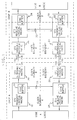
- FIG. 1 of the drawings it illustrates one embodiment in which a self-timed interface in accordance with the teachings of this invention can be used.
- This exemplary embodiment of the self-timed interface provides data communications between two microprocessor chips, labeled here as Chip A and Chip B.
- Chip A and Chip B are microprocessor chips
- the self-timed interface of this invention is applicable to provide data transfer between a wide variety of components or nodes.
- Chip A has a transmit port labeled 12A and Chip B has a transmit port labeled 12B.
- Chips A and B have receive ports labeled 14A and 14B, respectively.
- the ports are connected by two self-timed interface busses 16; one for each transmission direction.
- each bus 16 is one byte wide, and comprised of nine electrical conductors; eight conductors for data and one conductor for a clock signal.
- Each transmit port (12A and 12B) includes a transmit logical macro 18 that provides a logical interface between the host logic and the self-timed interface link 16.
- Sync buffers 22 provide an interface between the host clock and the self-timed interface clock. This allows the self-timed interface link to run at a predetermined cycle time that is independent of the host clock, making the self-timed interface link independent of the host.
- An outbound physical macro 24 serializes a word-wide data flow into a byte-wide data flow that is transmitted along with the clock on the self-timed interface link 16.
- Each receive port (i.e., 14A and 14B) includes an inbound physical macro 26 that first dynamically aligns each data bit with the self-timed interface clock signal. It aligns any bits with skew up to three bit cells and deserializes the bytes into words.
- a receive logical macro 28 provides an interface between the self-timed interface receiver logic and the host logic and generates link acknowledge signals and link reject signals, which are coupled by internal links 33 and transmitted back to the transmitting port via an outbound self-timed interface link 16. In order to compensate for variations in electrical path delay, the phase of the incoming data is adjusted, or self-timed.
- Each bit (line) is individually phase aligned to the transmitted reference clock and further aligned to compensate, within embodiment, for up to three bit cells of skew between any two data lines.
- the self-timing operation has three parts. The first is to acquire bit synchronization; the second is byte/word alignment; and the third is maintaining synchronization.
- the link takes itself from a completely untimed state into synchronous operation. Any previous condition on the STI interface or logic is disregarded with a complete logic reset.
- the bit synchronization process can be rapidly established, for example on the order of 200 microseconds.
- the phase of the incoming data is manipulated on a per line basis until the data valid window or bit interval is located. This is accomplished using a phase detector that locates an average edge position on the incoming data relative to the local clock. Using two phase detectors one can locate two consecutive edges on data and these two consecutive edges define the bit interval or data valid window.
- the data to be sampled by the local clock is the phase of the data located halfway between the two edges of the data.
- Byte alignment takes place by manipulating the serial data stream in whole bit times to properly adjust the byte position relative to a deserializer output.
- Word alignment takes place next by manipulating the deserializer data four bit intervals a time to ensure proper word synchronization on the STI interface. A timing sequence allows proper bit, byte and word synchronization.
- Synchronization maintenance occurs as part of the link operation in response to temperature and power supply variations.
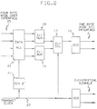
- FIG. 2 illustrates one embodiment of a transmit serializer for a bit serial byte parallel interface used in the practice of the invention.
- a four byte wide data register 23 receives parallel inputs 25 (bytes 0, 1, 2 and 3 inputs shown here) and multiplexes them to a one byte wide self-timed interface.
- Data is clocked from the register 23 by a divide by two of the self-timed interface clock on line 27.
- Bit zero from bytes 0, 1, 2 and 3 are serialized and transmitted on link 0 of the self-timed interface, shown here.
- Bit 1 from bytes 0, 1, 2 and 3 will be transmitted on link 1 (not shown)and so on.
- the STI clock is one half the frequency of the transmitted data (baud) rate, i.e., a 75 Mhz clock will be used for a 150 Mbit/S data rate.
- the clock will be generated from an STI oscillator source, this is done to decouple the system or host clock from the STI link.
- the data will be transmittedwith both edges of the clock.
- the deserializer data output for a particular data line is monitored for the expected timing pattern (X 0 1 0 where X is a don't care) to determine the proper order of the received data. If at any time a zero is detected in the bit 3 position the multiplexer is incremented thus moving the byte boundary by one bit time. This process is repeated until the proper byte boundary is located.
- the multiplexer control wraps around from a binary 3 to a binary 0 in case the correct position was incorrectly passed through the previous time. this function allows synchronization of data lines skewed by more than an entire bit time.
- the clock rate is the same as the data rate.
- the data edges that define a data window are each detected independently of the other and the data is sampled at the midpoint between the edges when the edges have been aligned with the clock.
- the position of the edges of incrementally separated phases of the input data stream are successively compared to the position of the rising and falling edges of the clock in order to locate the edges of the data stream with respect to both edges of the clock (e.g., the rising and falling edges).
- the data phase pairs are generated in this specific embodiment of the invention by three incrementally selectable delay elements 80, 82, and 84.
- the elements 80 and 82 provide delays, respectively, in 1/10th and 1/5th bit time increments and element 84 provides fine increments on the order of 1/20th of a bit time.
- the fine delay element 84 is separated into three groups to provide early edge detection, system data detection, and late edge detection.
- An early guard band selector 86 successively selects one phase of the data stream to provide an "early" phase of the incrementally separated phases - one for the rising edge and one for the falling edge.
- a late guard band selector 90 successively selects one phase of the data stream to provide a "late" phase of the incremental phases - again one for the rising edge and one for the falling edge.
- a selector 88 selects incremental phases for the mid-cell system data position.
- a selected data phase is coupled as an input to master-slave RES-FES latch pairs 92, 94, and 96.
- the rising edge data samples are clocked into the RES latches and the falling edge data samples are clocked into the FES latches.
- the outputs of the RES-FES latch pair 92 are connected to an early edge detector 98.
- the outputs of the RES-FES latch pair 96 are coupled to a late edge detector 100.
- the RES latch of pair 94 is coupled to the early edge detector 98 and the FES latch of pair 94 is coupled to the late edge detector 100.
- Each edge detector (98 and 100) outputs a "lead", a "lag” or a "do nothing" output which indicates the location of a data edge with respect to the reference clock edge location.
- the output of each edge detector is coupled via a suitable filter 102 (i.e., a random walk filter), back to its respective selector 86 and selector 90, respectively.
- the selectors shift the phase of the data coupled to the RES-FES latches in the direction indicated, or if "do nothing" is indicated, the phase of the data at that edge is not shifted.
- Data control logic 104 controls the system data output by selecting the phase of the data that is halfway between the two data edges when the data edges are aligned with the reference clock. A phase of the data (Data 1 and Data 2) is outputted at each reference clock edge.
- the edge detect circuitry will sample the incoming data with the received reference clock.
- the edge detector will output a "lead", a "lag” or a "do nothing" signal that indicates the data edge location relative to the reference clock.
- This signal is filtered by a Random Walk Filter (RWF) and fed-back to the selectors of their respective RES and FES circuits. The selectors shift the phase of the data into the RES and FES as indicated by the edge detector.
- RWF Random Walk Filter
- Each will locate the transitions on data relative to the received (ref) clock by manipulating the incoming phase of the data into the edge detector as described above.
- the phase of the system data is controlled by the data control logic which selects the phase of the data halfway between the two edge detectors.
- the order of bits out of the deserializer are manipulated to the correct order (see byte/word synchronization below).
- the 16 microsecond timer trips the algorithm resets a deserializer error latch and restarts the 16 microsecond counter.
- the deserializer output is compared against the expected timing pattern (X 0 1 0 where X is a don't care). A single miscompare on any cycle during the next 16 microseconds will set the deserializer error latch.
- the algorithm checks the addresses of the EGB, LGB, and data selectors, deserializer error latch.
- the deserializer output latch In order for a bit to end the initial bit synchronization search state, the deserializer output latch must have remained reset AND the all selectors must be properly centered in their tracking range (centering ensures that adjustments can be made to allow for the tracking of temp. and power supply variations after the initial bit synchronization process). If both conditions are not met then the algorithm adds a bulk delay element, resets the 16 microsecond counter and the search process begins once again. Each and every bit (data line) on the STI interface undergoes this process in parallel.
- Word alignment is established by manipulating the deserializer output bus four bits at a time until word synchronization is established. Note that the first register is shifted by four bit times relative to the second register. Four bit times is the maximum any data bit can be skewed relative to another data bit (3 bit times on link + 1 bit time from phase alignment section).
- the physical macro will continuously monitor the incoming data to ensure that the optimum clock sampling relationship exists. Small updates will be made to track temperature, power supply and data jitter. These updates will be seamless and transparent to the host logic. Approximately 1/2 a bit time of delay will be needed to compensate for temperature and power supply variations to maintain proper synchronization. This added delay is in the fine delay elements section.
- the circuitry that makes these on the fly bulk adjustments can be inhibited so no on the fly bulk delay adjustments are made during normal operation.
- the second case exists when one of the guard bands reaches the end of its range and the on the fly bulk delay adjustment is inhibited, the physical macro will signal the logical STI macro that a bit synchronization is required soon.
- the link should finish the immediate work and force the link into timing mode.
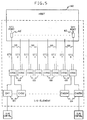
- a host processor 60 in this exemplary embodiment needs only eight STI ports 62 to support up to 256 input-output channels 65, which are in turn coupled to input-output controllers 65.
- STI links 66 couple the ports 62 to input-output sub-elements 68 labeled IOSE.
- the sub-elements 68 which may be integral with or physically located away from the host 60, each can support up to 32 channel functions.
- the extended operating length of the self-timed interface 66 i.e., up to ten meters without performance degradation) makes it possible to package this many channel functions in a cost effective manner.
- a single STI is capable of supporting 32 channel functions. For those system configurations requiring only up to 32 channels therefore, only one STI port, cable and I/O sub-element need be used. This enables incremental cost advantages over current centralized I/O elements in which even the smallest channel configuration can incur the cost of hardware in place for the maximum (e.g., 256) channel configuration.
- STI enables each I/O sub-element to operate asynchronously to the host clock, thereby avoiding the clock control complexity associated with the previously described variable clock multiplier logic. This permits the I/O sub-elements to be used by a wider range of hosts/host cycle times. Because of the high performance of STI, fewer are needed, thus the re-synchronizing buffers/logic at each end is not burdensome.
Landscapes
- Engineering & Computer Science (AREA)
- Theoretical Computer Science (AREA)
- Physics & Mathematics (AREA)
- General Engineering & Computer Science (AREA)
- General Physics & Mathematics (AREA)
- Information Transfer Systems (AREA)
- Communication Control (AREA)
- Synchronisation In Digital Transmission Systems (AREA)
Applications Claiming Priority (2)
| Application Number | Priority Date | Filing Date | Title |
|---|---|---|---|
| US08/261,561 US5513377A (en) | 1994-06-17 | 1994-06-17 | Input-output element has self timed interface using a received clock signal to individually phase aligned bits received from a parallel bus |
| US261561 | 2002-09-30 |
Publications (1)
| Publication Number | Publication Date |
|---|---|
| EP0687980A2 true EP0687980A2 (fr) | 1995-12-20 |
Family
ID=22993866
Family Applications (1)
| Application Number | Title | Priority Date | Filing Date |
|---|---|---|---|
| EP95105480A Withdrawn EP0687980A2 (fr) | 1994-06-17 | 1995-04-12 | Unité d'entrée-sortie |
Country Status (3)
| Country | Link |
|---|---|
| US (1) | US5513377A (fr) |
| EP (1) | EP0687980A2 (fr) |
| JP (1) | JPH088890A (fr) |
Cited By (2)
| Publication number | Priority date | Publication date | Assignee | Title |
|---|---|---|---|---|
| US6839861B2 (en) | 2001-07-30 | 2005-01-04 | International Business Machines Corporation | Method and system for selecting data sampling phase for self timed interface logic |
| DE10350388A1 (de) * | 2003-10-28 | 2005-06-02 | Micronas Gmbh | Bussystem mit wenigen Steuerleitungen |
Families Citing this family (45)
| Publication number | Priority date | Publication date | Assignee | Title |
|---|---|---|---|---|
| JP3490131B2 (ja) | 1994-01-21 | 2004-01-26 | 株式会社ルネサステクノロジ | データ転送制御方法、データプロセッサ及びデータ処理システム |
| EP0687986A3 (fr) * | 1994-06-17 | 1996-02-14 | Ibm | Méthode et appareil pour la transmission de données digitales dans des systèmes massivement parallèles |
| US5640605A (en) * | 1994-08-26 | 1997-06-17 | 3Com Corporation | Method and apparatus for synchronized transmission of data between a network adaptor and multiple transmission channels using a shared clocking frequency and multilevel data encoding |
| US5706484A (en) * | 1995-12-20 | 1998-01-06 | Intel Corporation | Method for eliminating transition direction sensitive timing skews in a source synchronous design |
| US5757297A (en) * | 1996-06-07 | 1998-05-26 | International Business Machines Corporation | Method and apparatus for recovering a serial data stream using a local clock |
| US5859881A (en) * | 1996-06-07 | 1999-01-12 | International Business Machines Corporation | Adaptive filtering method and apparatus to compensate for a frequency difference between two clock sources |
| US5872959A (en) * | 1996-09-10 | 1999-02-16 | Lsi Logic Corporation | Method and apparatus for parallel high speed data transfer |
| US6021503A (en) * | 1996-12-21 | 2000-02-01 | Micron Communications, Inc. | Bit synchronization for interrogator |
| DE19713660A1 (de) * | 1997-04-02 | 1998-10-08 | Siemens Nixdorf Inf Syst | Phasenjustierung schneller paralleler Signale |
| US5894570A (en) * | 1997-04-08 | 1999-04-13 | International Business Machines Corporation | System for initializing a self-timed link |
| US5968179A (en) * | 1997-04-08 | 1999-10-19 | International Business Machines Corporation | Method for initializing a self-timed link |
| US6262998B1 (en) * | 1997-12-24 | 2001-07-17 | Nortel Networks Limited | Parallel data bus integrated clocking and control |
| US6223317B1 (en) * | 1998-02-28 | 2001-04-24 | Micron Technology, Inc. | Bit synchronizers and methods of synchronizing and calculating error |
| TR200002649T2 (tr) | 1998-03-16 | 2000-11-21 | Jazio Inc. | VLSI CMOS arayüz devreleri için yüksek hızlı sinyal üretimi. |
| US6327205B1 (en) | 1998-03-16 | 2001-12-04 | Jazio, Inc. | Signal latching of high bandwidth DRAM arrays when skew between different components is higher than signal rate |
| US6160423A (en) * | 1998-03-16 | 2000-12-12 | Jazio, Inc. | High speed source synchronous signaling for interfacing VLSI CMOS circuits to transmission lines |
| JP3616247B2 (ja) * | 1998-04-03 | 2005-02-02 | 株式会社アドバンテスト | Ic試験装置におけるスキュー調整方法及びこれに用いる疑似デバイス |
| US6976083B1 (en) | 1999-02-19 | 2005-12-13 | International Business Machines Corporation | Apparatus for providing direct data processing access using a queued direct input-output device |
| US6397350B1 (en) * | 1999-02-19 | 2002-05-28 | International Business Machines Corporation | Method of providing direct data processing access using a queued direct input-output device |
| US6347341B1 (en) * | 1999-02-22 | 2002-02-12 | International Business Machines Corporation | Computer program product used for exchange and transfer of data having a siga vector and utilizing a queued direct input-output device |
| US6643752B1 (en) * | 1999-12-09 | 2003-11-04 | Rambus Inc. | Transceiver with latency alignment circuitry |
| US7266634B2 (en) | 2000-01-05 | 2007-09-04 | Rambus Inc. | Configurable width buffered module having flyby elements |
| US7404032B2 (en) * | 2000-01-05 | 2008-07-22 | Rambus Inc. | Configurable width buffered module having switch elements |
| US7017002B2 (en) * | 2000-01-05 | 2006-03-21 | Rambus, Inc. | System featuring a master device, a buffer device and a plurality of integrated circuit memory devices |
| US7356639B2 (en) | 2000-01-05 | 2008-04-08 | Rambus Inc. | Configurable width buffered module having a bypass circuit |
| US7363422B2 (en) * | 2000-01-05 | 2008-04-22 | Rambus Inc. | Configurable width buffered module |
| US6502161B1 (en) * | 2000-01-05 | 2002-12-31 | Rambus Inc. | Memory system including a point-to-point linked memory subsystem |
| US6725390B1 (en) * | 2000-06-29 | 2004-04-20 | Intel Corporation | Method and an apparatus for adjusting clock signal to sample data |
| US20020093986A1 (en) * | 2000-12-30 | 2002-07-18 | Norm Hendrickson | Forward data de-skew method and system |
| US20020091885A1 (en) * | 2000-12-30 | 2002-07-11 | Norm Hendrickson | Data de-skew method and system |
| US7123660B2 (en) * | 2001-02-27 | 2006-10-17 | Jazio, Inc. | Method and system for deskewing parallel bus channels to increase data transfer rates |
| US6907552B2 (en) * | 2001-08-29 | 2005-06-14 | Tricn Inc. | Relative dynamic skew compensation of parallel data lines |
| DE10344818B4 (de) * | 2003-09-27 | 2008-08-14 | Qimonda Ag | Vorrichtung zum Kalibrieren der relativen Phase zweier Empfangssignale eines Speicherbausteins |
| US6984991B2 (en) * | 2004-05-11 | 2006-01-10 | International Business Machines Corporation | Initialization of a bidirectional, self-timed parallel interface with automatic testing of AC differential wire pairs |
| US8112655B2 (en) * | 2005-04-21 | 2012-02-07 | Violin Memory, Inc. | Mesosynchronous data bus apparatus and method of data transmission |
| US9286198B2 (en) | 2005-04-21 | 2016-03-15 | Violin Memory | Method and system for storage of data in non-volatile media |
| US8452929B2 (en) * | 2005-04-21 | 2013-05-28 | Violin Memory Inc. | Method and system for storage of data in non-volatile media |
| US7401246B2 (en) * | 2005-06-30 | 2008-07-15 | Intel Corporation | Nibble de-skew method, apparatus, and system |
| US11328764B2 (en) | 2005-09-26 | 2022-05-10 | Rambus Inc. | Memory system topologies including a memory die stack |
| US7464225B2 (en) * | 2005-09-26 | 2008-12-09 | Rambus Inc. | Memory module including a plurality of integrated circuit memory devices and a plurality of buffer devices in a matrix topology |
| US7562271B2 (en) | 2005-09-26 | 2009-07-14 | Rambus Inc. | Memory system topologies including a buffer device and an integrated circuit memory device |
| US8028186B2 (en) * | 2006-10-23 | 2011-09-27 | Violin Memory, Inc. | Skew management in an interconnection system |
| US7624310B2 (en) * | 2007-07-11 | 2009-11-24 | Micron Technology, Inc. | System and method for initializing a memory system, and memory device and processor-based system using same |
| US9465756B2 (en) * | 2009-12-23 | 2016-10-11 | Violin Memory Inc. | Configurable interconnection system |
| US9213487B2 (en) * | 2013-10-16 | 2015-12-15 | Qualcomm Incorporated | Receiver architecture for memory reads |
Family Cites Families (15)
| Publication number | Priority date | Publication date | Assignee | Title |
|---|---|---|---|---|
| US4050097A (en) * | 1976-09-27 | 1977-09-20 | Honeywell Information Systems, Inc. | Synchronization technique for data transfers over an asynchronous common bus network coupling data processing apparatus |
| DE2936938C2 (de) * | 1979-09-12 | 1987-01-08 | Siemens AG, 1000 Berlin und 8000 München | Schaltungsanordnung zum Ausgleich der Phasenunterschiede zwischen dem Streckentakt auf einer mit einer PCM-Vermittlungsstelle verbindenden PCM-Zeitmultiplexleitung und dem Amtstakt dieser Vermittlungsstelle |
| US4694472A (en) * | 1982-04-26 | 1987-09-15 | American Telephone And Telegraph Company | Clock adjustment method and apparatus for synchronous data communications |
| GB8528890D0 (en) * | 1985-11-23 | 1986-01-02 | Int Computers Ltd | Data transmission system |
| US4771440A (en) * | 1986-12-03 | 1988-09-13 | Cray Research, Inc. | Data modulation interface |
| US5022057A (en) * | 1988-03-11 | 1991-06-04 | Hitachi, Ltd. | Bit synchronization circuit |
| JPH0267525A (ja) * | 1988-09-02 | 1990-03-07 | Hitachi Ltd | 光スイツチ装置及びスイツチ間伝送方法 |
| US4914429A (en) * | 1988-12-09 | 1990-04-03 | Transwitch Corp. | Switch components and multiple data rate non-blocking switch network utilizing the same |
| JPH02166918A (ja) * | 1988-12-21 | 1990-06-27 | Nec Corp | デイジタル位相調整回路 |
| JPH02192337A (ja) * | 1989-01-20 | 1990-07-30 | Fujitsu Ltd | 位相調整回路 |
| JPH03154239A (ja) * | 1989-11-10 | 1991-07-02 | Pioneer Electron Corp | 光ディスクカッティング装置 |
| US4965884A (en) * | 1989-11-22 | 1990-10-23 | Northern Telecom Limited | Data alignment method and apparatus |
| JPH05175945A (ja) * | 1991-12-25 | 1993-07-13 | Fujitsu Ltd | 無瞬断通信処理ユニット切り離し方式 |
| JPH0653955A (ja) * | 1992-04-21 | 1994-02-25 | Nec Corp | パラレルビット同期方式 |
| US5400370A (en) * | 1993-02-24 | 1995-03-21 | Advanced Micro Devices Inc. | All digital high speed algorithmic data recovery method and apparatus using locally generated compensated broad band time rulers and data edge position averaging |
-
1994
- 1994-06-17 US US08/261,561 patent/US5513377A/en not_active Expired - Lifetime
-
1995
- 1995-04-12 EP EP95105480A patent/EP0687980A2/fr not_active Withdrawn
- 1995-05-15 JP JP7115415A patent/JPH088890A/ja active Pending
Cited By (3)
| Publication number | Priority date | Publication date | Assignee | Title |
|---|---|---|---|---|
| US6839861B2 (en) | 2001-07-30 | 2005-01-04 | International Business Machines Corporation | Method and system for selecting data sampling phase for self timed interface logic |
| DE10350388A1 (de) * | 2003-10-28 | 2005-06-02 | Micronas Gmbh | Bussystem mit wenigen Steuerleitungen |
| US7634602B2 (en) | 2003-10-28 | 2009-12-15 | Micronas Gmbh | Bus system with few control lines |
Also Published As
| Publication number | Publication date |
|---|---|
| JPH088890A (ja) | 1996-01-12 |
| US5513377A (en) | 1996-04-30 |
Similar Documents
| Publication | Publication Date | Title |
|---|---|---|
| US5513377A (en) | Input-output element has self timed interface using a received clock signal to individually phase aligned bits received from a parallel bus | |
| US5832047A (en) | Self timed interface | |
| US5522088A (en) | Shared channel subsystem has a self timed interface using a received clock signal to individually phase align bits received from a parallel bus | |
| EP0522764B1 (fr) | Schéma de multiplexage pour signaux de contrôle de modem | |
| EP1397895B1 (fr) | Transmission en parallele avec codes de synchronisation multiples | |
| US4450572A (en) | Interface for serial data communications link | |
| KR950005147B1 (ko) | 패킷 통신용 패킷 스위칭 회로망 및 그것에 의한 패킷 스위칭 방법 | |
| US5694612A (en) | Self-timed interface for a network of computer processors interconnected in parallel | |
| EP1366422B1 (fr) | Methode et appareil de calibrage de canaux en temps reel | |
| US5598442A (en) | Self-timed parallel inter-system data communication channel | |
| EP0405756A2 (fr) | Réseau de données autocicatrisant et contrôleur de noeud de réseau | |
| EP0996262A1 (fr) | Système de communication comportant une pluralité de liaisons de données synchronisées | |
| KR102518285B1 (ko) | PCIe 인터페이스 및 인터페이스 시스템 | |
| JP2004520778A (ja) | スキュー耐性のないデータグループを有するパラレルデータ通信 | |
| WO1989009523A1 (fr) | Procede et appareil de transmission stabilisee de donnees | |
| US7340021B1 (en) | Dynamic phase alignment and clock recovery circuitry | |
| EP0141659B1 (fr) | Interface de communication | |
| US5502817A (en) | Ultra high speed data collection, processing and distribution ring with parallel data paths between nodes | |
| US6192482B1 (en) | Self-timed parallel data bus interface to direct storage devices | |
| EP0276076B1 (fr) | Commutateur de signaux numériques | |
| US6611538B1 (en) | Data transmission synchronization system | |
| US20020112111A1 (en) | Parallel and point-to-point data bus architecture | |
| AU682352C (en) | Ultra high speed data collection, processing and distribution ring with parallel data paths between nodes |
Legal Events
| Date | Code | Title | Description |
|---|---|---|---|
| PUAI | Public reference made under article 153(3) epc to a published international application that has entered the european phase |
Free format text: ORIGINAL CODE: 0009012 |
|
| AK | Designated contracting states |
Kind code of ref document: A2 Designated state(s): DE FR GB |
|
| STAA | Information on the status of an ep patent application or granted ep patent |
Free format text: STATUS: THE APPLICATION HAS BEEN WITHDRAWN |
|
| 18W | Application withdrawn |
Withdrawal date: 19960716 |