EP0688059B1 - Dielektrisches Filter - Google Patents
Dielektrisches Filter Download PDFInfo
- Publication number
- EP0688059B1 EP0688059B1 EP95401420A EP95401420A EP0688059B1 EP 0688059 B1 EP0688059 B1 EP 0688059B1 EP 95401420 A EP95401420 A EP 95401420A EP 95401420 A EP95401420 A EP 95401420A EP 0688059 B1 EP0688059 B1 EP 0688059B1
- Authority
- EP
- European Patent Office
- Prior art keywords
- excitation
- holes
- dielectric
- hole
- external coupling
- Prior art date
- Legal status (The legal status is an assumption and is not a legal conclusion. Google has not performed a legal analysis and makes no representation as to the accuracy of the status listed.)
- Expired - Lifetime
Links
- 230000005284 excitation Effects 0.000 claims description 131
- 239000004020 conductor Substances 0.000 claims description 110
- 230000008878 coupling Effects 0.000 claims description 93
- 238000010168 coupling process Methods 0.000 claims description 93
- 238000005859 coupling reaction Methods 0.000 claims description 93
- 230000005540 biological transmission Effects 0.000 claims description 5
- 239000000758 substrate Substances 0.000 description 17
- 230000001965 increasing effect Effects 0.000 description 10
- 238000004806 packaging method and process Methods 0.000 description 10
- 238000003780 insertion Methods 0.000 description 4
- 230000037431 insertion Effects 0.000 description 4
- 230000003247 decreasing effect Effects 0.000 description 3
- 230000005672 electromagnetic field Effects 0.000 description 3
- 238000005452 bending Methods 0.000 description 2
- 230000002950 deficient Effects 0.000 description 2
- 238000002474 experimental method Methods 0.000 description 2
- 230000001939 inductive effect Effects 0.000 description 2
- 238000004519 manufacturing process Methods 0.000 description 2
- 239000002184 metal Substances 0.000 description 2
- 238000000034 method Methods 0.000 description 2
- 239000000126 substance Substances 0.000 description 2
- 238000013459 approach Methods 0.000 description 1
- 238000010420 art technique Methods 0.000 description 1
- 239000003990 capacitor Substances 0.000 description 1
- 230000001413 cellular effect Effects 0.000 description 1
- 230000001419 dependent effect Effects 0.000 description 1
- 230000002542 deteriorative effect Effects 0.000 description 1
- 239000003989 dielectric material Substances 0.000 description 1
- 238000010295 mobile communication Methods 0.000 description 1
- 238000003825 pressing Methods 0.000 description 1
- 238000005096 rolling process Methods 0.000 description 1
- 238000005476 soldering Methods 0.000 description 1
Images


Classifications
-
- H—ELECTRICITY
- H01—ELECTRIC ELEMENTS
- H01P—WAVEGUIDES; RESONATORS, LINES, OR OTHER DEVICES OF THE WAVEGUIDE TYPE
- H01P1/00—Auxiliary devices
- H01P1/20—Frequency-selective devices, e.g. filters
- H01P1/213—Frequency-selective devices, e.g. filters combining or separating two or more different frequencies
- H01P1/2136—Frequency-selective devices, e.g. filters combining or separating two or more different frequencies using comb or interdigital filters; using cascaded coaxial cavities
-
- H—ELECTRICITY
- H01—ELECTRIC ELEMENTS
- H01P—WAVEGUIDES; RESONATORS, LINES, OR OTHER DEVICES OF THE WAVEGUIDE TYPE
- H01P1/00—Auxiliary devices
- H01P1/20—Frequency-selective devices, e.g. filters
- H01P1/201—Filters for transverse electromagnetic waves
- H01P1/205—Comb or interdigital filters; Cascaded coaxial cavities
- H01P1/2056—Comb filters or interdigital filters with metallised resonator holes in a dielectric block
Definitions
- the present invention relates to a dielectric filter for use in a mobile communication device such as a cellular telephone or other portable telephone.
- a prior art dielectric filter comprising a dielectric block 1 is shown in Fig. 14.
- the shaded portions indicate visible parts of the dielectric material of the dielectric block. On these visible portions, no conductor is formed.
- this dielectric filter has, for example, two resonator holes 2 extending between a pair of opposite end surfaces of the dielectric filter, indicated by reference numerals 1a and 1b.
- Inner conductors 3 are formed on the inner surfaces of the resonator holes 2.
- An outer conductor 4 is formed on the outer surface of the block 1.
- a pair of input/output electrodes 7 are formed at desired locations on the outer surface of the dielectric block.
- the inner conductors 3 are not formed at portions (hereinafter referred to as nonconductive portions) close to one "open" surface 1a (hereinafter referred to as the open end surface) of the openings of the resonator holes 2. These nonconductive portions are isolated from the outer conductor 4.
- the inner conductors 3 are electrically connected or shorted to the outer conductor 4.
- This dielectric filter consists of two stages of resonators each of which is formed in a respective one of the resonator holes 2. These resonators are interconnected in a so-called comb-line connection coupling by stray capacitance created in the nonconductive portions.
- an external coupling capacitance Ce is produced between each input/output electrode 7 and the corresponding inner conductor 3, as shown in Fig. 14.
- This external coupling capacitance Ce provides external coupling.
- phase-adjusting wave-separating circuit When an antenna filter is constructed by using two such dielectric filters, a phase-adjusting wave-separating circuit is inserted between one filter end and an antenna end acting as the common input/output end of both filters, so that the phase of reflected waves in the passband of the opposite filter will cause the opposite filter to appear as an open circuit.
- a lumped constant device such as a capacitive device or an inductive device or a distributed constant line such as cable or stripline is used as the wave-separating circuit.
- the area of the input/output electrodes may be increased.
- the resonator holes may be positioned in eccentric positions to shorten the distance between each input/output electrode and the corresponding inner conductor. In this way, adequate external coupling is derived.
- the unloaded Q (or, Q o ) of each resonator drops.
- an increase in the area of the input/output electrodes reduces the effective dielectric constant, thus increasing the resonator's electrical length.
- phase-adjusting components such as capacitors, coils, or striplines are required in addition to the dielectric filters.
- some operation for mounting and soldering them to a substrate or for forming them on a substrate is required. Consequently, it is difficult to miniaturize the antenna filter. Hence, the cost of the components or fabrication cost is increased.
- the phase of the filter is also determined. This makes it impossible to set external coupling and phase independently. In consequence, it is difficult to obtain a particular desired degree of external coupling and a particular desired phase simultaneously. Where a desired phase is associated with connection to another filter or external circuit, it is necessary to add a separate part for adjusting the phase.
- US-A-4 559 508 discloses the features as defined in the preamble of claim 1.
- the present invention is intended to solve the foregoing problems with the prior art techniques. It is an object of the invention to provide a dielectric filter permitting one to obtain appropriate external coupling easily without modifying the shape or dimensions of the input/output electrodes and/or without decreasing the Q o of the resonators.
- a first feature of the invention which lies in a dielectric filter comprising: a dielectric block having two opposite end surfaces and an outer surface; resonator holes formed in the dielectric block between said end surfaces and acting as input/output stages; inner conductors formed on inner surfaces of the resonator holes, respectively; and an outer conductor formed on the outer surface of the dielectric block.
- This dielectric filter is characterized in that excitation holes are formed in the block adjacently to the resonator holes and have inner conductors formed inside the excitation holes, and that the excitation holes are electromagnetically coupled to the resonator holes acting as the input/output stages, respectively, thereby providing external coupling.
- a second feature of the invention lies in a dielectric filter comprising: a dielectric block having two opposite end surfaces and an outer surface; resonator holes formed in the dielectric block between said end surfaces and acting as input/output stages; inner conductors formed on inner surfaces of the resonator holes, respectively; and an outer conductor formed on the outer surface of the dielectric block.
- This dielectric filter is characterized in that excitation holes are formed in the block adjacently to the resonator holes acting as the input/output stages and have inner conductors formed inside the excitation holes, and that the positions, shapes, or sizes of the excitation holes have been so set that desired external coupling and phase are obtained.
- a third feature of the invention lies in a dielectric filter comprising: a dielectric block having two opposite end surfaces and an outer surface; resonator holes formed in the dielectric block between said end surfaces; inner conductors formed on inner surfaces of the resonator holes, respectively; and an outer conductor formed on the outer surface of the dielectric block.
- This dielectric filter is characterized in that excitation holes are formed in the block adjacently to the resonator holes and have inner conductors formed inside the excitation holes, and that external coupling-adjusting holes are formed in the block close to the excitation holes, respectively, acting as input/output stages and have inner conductors formed on inner surfaces of the external coupling-adjusting holes, respectively.
- a fourth feature of the invention is based on any one of the first through third features described above and characterized in that input/output electrodes are formed on one end surface of the dielectric block or extend from this end surface to one side surface of the dielectric block, are electrically connected with the inner conductors formed inside the excitation holes, and are disconnected from the outer conductor.
- a fifth feature of the invention is based on any one of the first through third features described above and characterized in that the dielectric block has regions in which said excitation holes are formed, and that the regions have been partially removed so that one end surface of the dielectric block has steps.
- a sixth feature of the invention is based on any one of the first through third features described above and characterized in that the inner conductors formed inside the excitation holes or the inner conductors formed inside the external coupling-adjusting holes have been partially removed to adjust external coupling and phase.
- a seventh feature of the invention is based on any one of the first through third features described above and characterized in that there is further provided input/output terminals which are inserted in the excitation holes and electrically connected with the inner conductors formed inside the excitation holes.
- An eighth feature of the invention is based on any one of the first through third features described above and characterized in that there is further provided a metallic casing mounted on the dielectric block so as to cover at least a part of the block.
- the excitation holes are electromagnetically coupled to their respective resonator holes, whereby the filter provides external coupling.
- the degree of the external coupling is adjusted or set by varying the diameters or positions of the excitation holes.
- the excitation holes are electromagnetically coupled to their respective resonator holes, whereby the filter provides external coupling. Desired external coupling and phase can be established by varying the positions, the shapes, or the sizes of the excitation holes.
- desired external coupling is provided by varying the positions, the shapes, or the sizes of the external coupling-adjusting holes. That is, the external coupling can be established with greater degree of freedom because the external coupling-adjusting holes are provided. Where resonator holes are formed on opposite sides of each excitation hole, the coupling between two resonator holes on opposites sides of at least one excitation hole can be suppressed.
- the filter can be connected with an external circuit, or a packaging substrate, through the input/output electrodes electrically connected with the conductors formed inside the excitation holes.
- These input/output electrodes are not intended to provide external coupling. Rather, the shapes and the dimensions of these electrodes can be set at will. That is, the shapes and the dimensions can be set in such a way that the characteristics such as Q o are not deteriorated.
- the input/output electrodes are designed to extend from one end surface to one side surface, any one of the end surface and/or the side surface can be used as a mounting surface. That is, the dielectric filter can be placed either horizontally or vertically.
- the conductors inside the excitation holes or the conductors inside the external coupling-adjusting holes have been partially removed.
- the external coupling and phase can be adjusted.
- the dielectric block has been partially removed, so that the length of the excitation holes is adjusted.
- the degree of external coupling can be varied by varying the length of the excitation holes 5, as well as the diameter or the positions of the holes 5. Therefore, the external coupling can be adjusted or established with greater degree of freedom. Hence, more appropriate external coupling can be obtained.
- the filter can be connected with an external circuit, or a packaging substrate, via input/output terminals electrically connected with the conductors formed inside the excitation holes. That is, the filter can be mounted on a terminal insertion type packaging substrate.
- the dielectric filter can be placed either horizontally or vertically by bending the input/output terminals. Furthermore, the location at which the connection with the packaging substrate is made can be set at will by varying the length of the input/output terminals. In this case, it is not necessary to form input/output electrodes. The characteristics such as Q o can be improved further.
- leakage of electro-magnetic field from the openings of the resonator holes can be reduced by mounting a metallic casing on the filter.
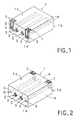
- this dielectric filter comprises a dielectric block 1 taking the form of a substantially rectangular parallelepiped.
- Two resonator holes 2 and a pair of excitation holes 5 are formed in the block 1.
- the resonator holes 2 extend between two opposite end surfaces of the block.
- Inner conductors 3 are formed on the inner surfaces of the resonator holes 2 and excitation holes 5, respectively.
- An outer conductor 4 is formed substantially over the whole surface of the dielectric block 1.
- the excitation holes 5 are formed outside the resonator holes 2, respectively.
- a pair of input/output electrodes 7 extend from the open end surface 1a to one side surface 1c (the top surface in the figure).
- the electrodes 7 are electrically connected with inner conductors 3 but disconnected from the outer conductor 4. That is, the inner conductors 3 in the excitation holes 5 are disconnected from the outer conductor 4 at the open end surface 1a and electrically connected with the outer conductor 4 at the shorted end surface 1b.
- Nonconductive portions are formed in the inner conductors 3 inside the resonator holes 2 near the open end surface 1a. At the shorted end surface 1b, the inner conductors 3 are electrically connected or shorted to the outer conductor 4. Resonators formed by the resonator holes 2, respectively, are connected to each other in so-called comb-line connection by stray capacitance created in the nonconductive portions.
- the excitation holes 5 and their respective adjacent resonator holes 2 are electromagnetically coupled together.
- This electromagnetic coupling provides external coupling of the input/output portions of the dielectric filter.
- the input/output electrodes 7 are formed simply to make a connection with an external circuit.
- the degree of the external coupling can be adjusted or established by varying the distance between the conductor 3 inside each excitation hole 5 and the conductor 3 inside the adjacent resonator hole 2, which is accomplished by varying the inside diameter or the position of the excitation hole 5. That is, if the inside diameter of each excitation hole 5 is increased, or if it is brought closer to the resonator hole 2, then the distance between the adjacent inner conductors is reduced. This provides stronger external coupling.
- the external coupling is determined neither by the shape nor by the dimensions of the input/output electrodes 7. Therefore, even if it is desired to obtain external coupling of different strengthes, the shape and the dimensions of the input/output electrodes 7 can still be set at will. Hence, the input/output electrodes 7 can be standardized. This permits standardization of patterns on packaging substrates. As a result, costs of mounting can be curtailed.
- the area of the input/output electrodes can be reduced and so the drop in Q o , which would normally be caused by large input/output electrodes, does not take place. Additionally, an increase in resonator electrical length which would normally be caused by a decrease in effective dielectric constant is prevented. Moreover, it is not necessary to place the resonator holes 2 in greatly eccentrically shifted positions. Consequently, the drop in Q o , which would normally be caused by eccentric positioning of the resonator holes 2, can be suppressed. Hence, a small-sized dielectric filter which has high Q o , produces only a small amount of insertion loss, and provides desired external coupling can be obtained.
- the input/output electrodes 7 are so formed as to extend from the open end surface 1a to one side surface 1c, either the open end surface 1a or the side surface 1c can be mounted on a packaging substrate. That is, the dielectric filter of the present example can be placed either horizontally or vertically on the packaging substrate.
- a dielectric filter according to a second example of the invention is shown in Fig. 2.
- this dielectric filter is similar to the dielectric filter already described in connection with Fig. 1 except that a pair of input/output electrodes 7 extend from the shorted end surface 1b to one side surface 1c (the top surface in the figure) and are electrically connected with the inner conductors 3 in the excitation holes 5, respectively, but are disconnected from the outer conductor 4. That is, the conductors 3 inside the excitation holes 5 are electrically connected with the outer conductor 4 at the open end surface 1a but isolated from the outer conductor 4 at the shorted end surface 1b.
- the input/output electrodes 7 are formed on the side of the shorted end surface 1b in an opposite relation to the structure of the first example previously described in conjunction with Fig. 1.
- this second example can provide stronger external coupling, or stronger electromagnetic coupling, than the first example.
- the degree of external coupling can be adjusted or set by varying the diameter or positions of the excitation holes 5 without changing the positions or dimensions of the input/output electrodes 7 or the positions of the resonator holes 2. This makes it easy to standardize the input/output electrodes 7. Also, the Q o is prevented from dropping.
- the inner conductors 3a in the excitation holes 5 are electrically connected with the outer conductor 4 at one end of each excitation hole 5.
- This structure can provide stronger external coupling, or stronger electromagnetic coupling, than a structure in which the excitation holes 5 are electrically disconnected from the outer conductor 4.
- the input/output electrodes 7 extend from one end surface of the dielectric block 1 to an adjacent side surface.
- the electrodes may be formed only on one end surface.
- the electrodes may extend from the top side surface to the bottom side surface across one end surface.
- each electrode may extend from one end surface to two adjacent side surfaces which are perpendicular to each other.
- any one of the three surfaces on which the input/output electrodes 7 are formed may be used as a mounting surface and attached to a mounting substrate.
- the excitation holes 5 are formed substantially along the center line passing through the center of the dielectric block 1 in the direction of the thickness. As shown in Fig. 5, the excitation holes 5 may be shifted from the center line toward the top or bottom side of the dielectric block 1. No restrictions are imposed on the vertical positions of the excitation holes 5 in the dielectric block 1.
- a dielectric filter (antenna duplexer) according to a third example of the invention is shown in Fig. 6.
- five resonator holes 2a, 2b, 2c, 2d, and 2e extend between a pair of end surfaces of a dielectric block 1.
- An excitation hole 5a is formed outside the resonator hole 2a.
- Another excitation hole 5b is formed between the resonator holes 2b and 2c.
- a further excitation hole 5c is formed outside the resonator hole 2e.
- Inner conductors 3 are formed on the inner surfaces of the resonator holes 2a-2e and on the inner surfaces of the excitation holes 5a, 5b, and 5c, respectively.
- An outer conductor 4 is formed substantially over the whole outer surface of the dielectric block 1.
- Three input/output electrodes 7a, 7b, and 7c extend from the open end surface 1a to one side surface 1c and are electrically connected with the inner conductors 3 in the excitation holes 5a-5c but disconnected from the outer conductor 4.
- the inner conductors 3 in the excitation holes 5a, 5b, and 5c are electrically connected with the outer conductor 4 at the shorted end surface 1b.
- the inner conductors 3 in the resonator holes 2a-2e are disconnected from the outer conductor 4 by nonconductive portions at the open end surface 1a.
- the inner conductors 3 are electrically connected with the outer conductor 4 at the shorted end surface 1b.
- two resonators formed by the resonator holes 2a and 2b cooperate to form a transmission filter or reception filter.
- Three resonators formed by the resonator holes 2c, 2d, and 2e constitute a reception filter or transmission filter.
- the excitation holes 5a and 5c are electromagnetically coupled to the resonator holes 2a and 2e, respectively.
- the excitation hole 5b is electromagnetically coupled to the adjacent resonators 2b and 2c. These electromagnetic couplings provide external coupling.
- the input/output electrodes 7a, 7b, and 7c are formed simply for external connection with an external circuit.
- the input/output electrode 7b between the resonator holes 2b and 2c is an antenna electrode shared by the inputs and outputs of the transmission and reception filters.
- external coupling is provided by electromagnetic coupling between each excitation hole 5a, 5b, or 5c and the adjacent resonator hole 2a, 2b, 2c, 2d, or 2e. Therefore, the degree of external coupling can be adjusted or set by varying the diameters or positions of the excitation holes 5a, 5b, and 5c without changing the positions or dimensions of the input/output electrodes 7 or the positions of the resonator holes 2a-2e. Consequently, the input/output electrodes 7 can be standardized with ease. Also, Q o is prevented from decreasing. The characteristics of the filter can thereby be improved.
- the phase as well as external coupling can be set, by varying the positions, the shape or the internal diameter of the excitation holes. That is, the phase can be varied while maintaining the external coupling constant.
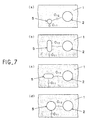
- Figs. 7(a)-7(d) are schematic cross sections of dielectric filters, taken close to the location of one excitation hole. These figures illustrate a method of establishing the self-capacitance C 11 of the excitation hole 5 formed between the conductor inside the excitation hole 5 and the outer conductor and the mutual capacitance C 12 created between the excitation hole 5 and the conductor inside the resonator hole 2.
- the excitation hole 5 is shifted toward either the upper or lower side of the dielectric block. In this illustrated example, the hole is shifted toward the lower side, to increase the self-capacitance C 11 and to reduce the mutual capacitance C 12 .
- the excitation hole 5 assumes substantially an elliptical shape.
- the self-capacitance C 11 and the mutual capacitance C 12 can be set to various values by varying the longitudinal direction of the excitation hole 5.
- the inside diameter of the excitation hole 5 is increased to increase both self-capacitance C 11 and mutual capacitance C 12 . In this way, the self-capacitance C 11 and mutual capacitance C 12 can be changed by varying the position, shape, or size of the excitation hole.
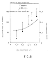
- Fig. 8 shows results of measured reflection phases about this filter having a center frequency of 836.5 MHz in the passband of the opposite filter, the passband lying in the frequency range of 869 to 894 MHz.
- the relation between the self-capacitance C 11 of the excitation hole and the mutual capacitance C 12 obtained where the external coupling is constant is indicated by triangles ⁇ .
- the relation between the self-capacitance C 11 and the reflection phase at 869 MHz is indicated by white circles O.
- the relation between the self-capacitance C 11 and the reflection phase at 894 MHz is indicated by black circles ⁇ .
- the external coupling can be maintained constant by varying the position, the shape, or other factor of the excitation hole so as to vary the self-capacitance C 11 and the mutual capacitance C 12 . That is, the reflection phase can be reduced while maintaining the external coupling constant, by reducing both self-capacitance C 11 and mutual capacitance C 12 . In other words, the reflection phase can be made to approach the open state.
- an antenna filter is built using such dielectric filters, if the positions, the shapes, or the sizes of the excitation holes in one filter corresponding to an antenna end are varied, then the reflection phase in the passband of the opposite filter can be made to assume an open state. Consequently, an antenna filter can be easily built without adding separate phase-adjusting components such as capacitive devices, inductive devices, or striplines.
- an antenna filter can be constructed simply by using two such dielectric filters or by using one such dielectric filter together with the prior art dielectric filter shown in Fig. 14 and then directly interconnecting respective input or output electrodes of the two filters.
- each excitation hole can be shaped into any desired form.
- the cross-sectional shape of the hole can be an ellipse, rectangle, triangle, or any other form.
- the dielectric filter is composed of two stages of resonators.
- the filter may also consist of only one stage of resonator.
- the filter may be made up of three or more stages of resonators.
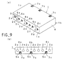
- Figs. 9(a) and 9(b) The structure of a dielectric filter (antenna duplexer) according to a fourth example of the invention is shown in Figs. 9(a) and 9(b).
- Fig. 9(a) is a perspective view of the dielectric filter (antenna duplexer) as viewed from the side of the open end surface.
- the bottom surface forming a mounting surface is here shown located at the top of the Figure.
- Fig. 9(b) is a plan view of the shorted end surface.
- the bottom surface forming a mounting surface is here shown located at the bottom of the Figure.
- the dielectric filter (antenna filter) of the present example comprises a dielectric block 1 substantially in the form of a rectangular parallelepiped.
- This block has a pair of opposite end surfaces 1a and 1b.
- Seven resonator holes 2a-2g extend between these end surfaces 1a and 1b.
- An excitation hole 5a and an external coupling-adjusting hole 6a are formed between the resonator holes 2a and 2b.
- An excitation hole 5b and an external coupling-adjusting hole 6b are formed between the resonator holes 2c and 2d.
- An excitation hole 5c and an external coupling-adjusting hole 6c are formed between the resonator holes 2f and 2g.
- Conductors 3 are formed on the inner surfaces of the resonator holes 2a-2g and on the inner surfaces of the external coupling-adjusting holes 6a-6c.
- An outer conductor 4 is formed substantially over the whole surface of the outer surface of the dielectric block 1.
- Three input/output electrodes 7a, 7b, and 7c extend from the shorted end surface 1b to one side surface, or the bottom surface.
- the input/output electrodes 7a, 7b, and 7c are electrically connected with the conductors 3 inside the excitation holes 5a-5c but isolated from the outer conductor 4. That is, the conductors 3 inside the excitation holes 5a-5c are electrically connected with the outer conductor 4 at the open end surface 1a and disconnected from the outer conductor 4 at the shorted end surface 1b.
- the conductors 3 inside the resonator holes 2a-2e are disconnected from the outer conductor 4 by nonconductive portions formed in the inner conductors close to the open end surface 1a and electrically connected with the outer conductor 4 at the shorted end surface 1b.
- the external coupling-adjusting holes 6a, 6b, and 6c are formed close to the excitation holes 5a, 5b, and 5c, respectively.
- the array of the adjusting holes 6a-6c is parallel to the array of the excitation holes 5a-5c.
- the conductors 3 formed inside the external coupling-adjusting holes 6a, 6b, and 6c are electrically connected with the outer conductor 4 at the open end surface 1a, as well as at the shorted end surface 1b. That is, the conductors 3 inside the adjusting holes 6a-6c act as grounding conductors similarly to the outer conductor 4.
- the excitation hole 5a is electromagnetically coupled to the adjacent resonator holes 2a and 2b.
- the excitation hole 5b is electromagnetically coupled to the adjacent resonator holes 2c and 2d.
- the excitation hole 5c is electromagnetically coupled to the adjacent resonator holes 2f and 2g. External coupling is provided by these electromagnetic couplings.
- the filter is connected with an external circuit via the input/output electrodes 7a, 7b, and 7c which are electrically connected with the conductors 3 inside the excitation holes 5a-5c.
- the input/output electrode 7b is an antenna electrode acting as one input/output of a transmission filter and also as one input/output of a reception filter.
- the self-capacitance of each excitation hole can be increased and/or reduced by varying the location, shape, or inside diameter of the external coupling-adjusting hole formed close to the excitation hole. Therefore, the external coupling can be modified, and external coupling can be established more appropriately. That is, the external coupling can be established with a greater degree of freedom by adding the external coupling-adjusting holes.
- the self-capacitance of each excitation hole is the capacitance created between the conductor inside the excitation hole and the grounding conductor, or the outer conductor plus the conductor inside the external coupling-adjusting hole.
- the self-capacitance of each excitation hole can be increased by providing the external coupling-adjusting hole. By reducing the distance between the excitation hole and the external coupling-adjusting hole, the self-capacitance of the excitation hole can be increased, and the external coupling can be weakened. Conversely, by increasing the distance between the excitation hole and the external coupling-adjusting hole, the self-capacitance of the excitation hole can be reduced and the external coupling can be intensified.
- the external coupling can be weakened by providing the external coupling-adjusting holes in this way, the distance between each excitation hole and the adjacent resonator hole can be reduced. Hence, the size of the filter can be reduced. That is, in the present example, the distance between the resonator holes 2a and 2b, the distance between the resonator holes 2c and 2d, and the distance between the resonator holes 2f and 2g can be reduced.
- the coupling between two resonator holes between which one excitation hole and one external coupling-adjusting hole are located can be suppressed by the external coupling-adjusting hole.
- direct coupling between the resonator holes 2a and 2b, direct coupling between the resonator holes 2c and 2d, and direct coupling between the resonator holes 2f and 2g can be suppressed by the external coupling-adjusting holes 6a, 6b, and 6c, respectively.
- direct coupling of the trap formed by the resonator hole 2a can be reduced greatly.
- the self-capacitance or other factor of each excitation hole can be varied by grinding parts of the conductors either in the excitation holes or in the external coupling-adjusting holes with a grinding tool or grindstone. In this manner, the external coupling and phase can be adjusted. Therefore, the characteristics can be improved. Also, the percentage of defective products can be reduced. In this case, the dielectric substance can be ground together with the inner conductors.
- one external coupling-adjusting hole is formed corresponding to each one excitation hole.
- the present invention is not limited to this structure.
- a plurality of external coupling-adjusting holes may be formed corresponding to each one excitation hole.
- the external coupling-adjusting holes may be shaped into any arbitrary form, which can be an ellipse, rectangle, triangle, or rhomboid.
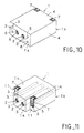
- the dielectric filter or antenna resonator has a complicated structure. It is to be noted that the present invention is not restricted to this structure. This example of the present invention is also applicable to a dielectric filter comprising a dielectric block 1 in which one filter is formed, as shown in Fig. 10.
- the dielectric block 1 is provided with two resonator holes 2.
- Excitation holes 5 and external coupling-adjusting holes 6 are formed outside their respective resonator holes 2.
- the degree of external coupling can be varied by varying the position, shape, or inside diameter of each external coupling-adjusting hole.
- the external coupling and phase can be adjusted by grinding parts of conductors formed inside the excitation holes and inside the external coupling-adjusting holes.
- the number of resonator holes formed in the dielectric block can be unity.
- every excitation hole has at least one corresponding external coupling-adjusting hole or holes.
- the invention is not limited to this structure.
- Each external coupling-adjusting hole may be formed for fewer than the full set of excitation holes, e.g. for at least one of the excitation holes.
- this dielectric filter comprises a dielectric block 1 having an open end surface 1a and one side surface 1c.
- This block has recessed portions 11 in which excitation holes 5 are formed on the side of the open end surface 1a.
- the open end surface 1a has a stepped shape.
- Each input/output electrode 7 extends from the corresponding recessed surface 11 to the side surface 1c.
- the excitation holes 5 extend from the recessed surfaces 11.
- the electrodes 7 are electrically connected with conductors 3 formed inside the excitation holes 5, respectively, and disconnected from an outer conductor 4.
- This dielectric filter is similar in structure to the dielectric filter already described in connection with Fig. 1 except for these points and so those components which have already been described are not described here.
- the degree of coupling due to the electromagnetic coupling of each excitation hole 5 to the adjacent resonator hole 2 can be adjusted and set by varying the length of the excitation hole 5. That is, the degree of external coupling can be changed by varying the length of the excitation holes 5, as well as the diameter of the holes 5 and the positions of the holes 5. Hence, the external coupling can be adjusted and set with a greater degree of freedom. As a result, more appropriate external coupling can be derived.
- steps are formed on the side of the open end surface 1a.
- the invention is not restricted to this structure.
- the steps may alternatively be formed on the side of the shorted end surface 1b.
- steps may be formed on both end surfaces 1a and 1b.
- the other examples above of a dielectric filter or antenna filter may also be modified to have these recessed surfaces 11.
- a dielectric filter according to a sixth example of the invention is shown in Fig. 12.
- this dielectric filter has an open end surface 1a on which input/output electrodes 7 are formed.
- the filter is provided with excitation holes 5, and conductors 3 are formed inside the holes 5, respectively.
- Input/output terminals 20 which are electrically connected with the conductors 3 inside the holes 5 are brought out from the open end surface 1a.
- Each input/output terminal 20 is a rodlike member made of a metal.
- These terminals 20 are respectively inserted into the excitation holes 5, and respectively soldered to the conductors 3 inside the excitation holes 5 or to the input/output electrodes 7, when the terminals 20 are mounted.
- This dielectric filter is similar in structure to the dielectric filter previously described in conjunction with Fig. 1 except for these points. That is, this dielectric filter is similar to the dielectric filter shown in Fig. 1 except that the input/output terminals 20 are connected.
- This structure can be mounted on a mounting substrate of the terminal insertion type.
- the dielectric filter can be placed either horizontally or vertically by bending the input/output terminals 20. Furthermore, the locations at which the filter is connected with the packaging substrate can be set at will by varying the length of the input/output terminals 20.
- the input/output electrodes 7 can be made smaller. Alternatively, the characteristics such as Q o can be improved further without the need to form the input/output electrodes 7.
- each input/output terminal 20 can be inserted into the excitation holes 5, respectively, from the end surface on which the input/output electrodes 7 are formed, and then the terminals 20 are connected. Moreover, restrictions are imposed neither on the shape of the input/output terminals 20 nor on the manner in which the terminals 20 are connected with the conductors 3 inside the excitation holes 5. For instance, each input/output terminal can be fabricated by rolling a sheet metal plate into a tube and pressing it against the conductors 3 inside the excitation holes 5 for connection.
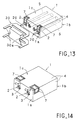
- a dielectric filter according to a seventh example of the invention is shown in Fig. 13.
- this dielectric filter has an open end surface 1a into which input/output terminals 20 are inserted.
- a metallic casing 30 is mounted on the dielectric block 1 so as to cover the open end surface 1a.
- the metallic casing 30 is soldered to the outer conductor 4, thus constructing the dielectric filter.
- Parts of the metallic casing 30 have apertures to permit the input/output terminals 20 to be brought out and to prevent the casing 30 from touching the input/output electrodes 7.
- This dielectric filter is similar in structure to the filter shown in Fig. 12 except for these points. That is, this example of dielectric filter is similar to the sixth example of dielectric filter shown in Fig. 12 except that the metallic casing 30 is mounted on it.
- a substrate may be inserted between the open end surface 1a and the metallic casing 30.
- this dielectric filter When this dielectric filter is mounted on a packaging substrate, input/output terminals 20 and protruding portions 30a of the metallic casing 30 are inserted into the packaging substrate.
- the open end surface 1a is covered with the metallic casing 30 and so leakage of electromagnetic field through the opening of each resonator hole 2 can be reduced.
- This metallic casing 30 can also be mounted to other examples of dielectric filter.
- coupling between adjacent resonators is provided by stray capacitance created in nonconductive portions in the inner conductors.
- the invention is not limited to this structure. Coupling holes or other coupling means may also be used to couple together the adjacent resonators.
- the manner in which the conductors inside the resonator holes are disconnected from the outer conductor at the open end surface is not limited to the method of the illustrated examples.
- the input/output portions are provided with excitation holes.
- External coupling is provided by electromagnetic coupling of each excitation hole to the adjacent resonator hole.
- the best external coupling can be obtained by appropriately establishing the inside diameter, positions, or the length of the excitation holes so as to adjust or establish the degree of external coupling.
- external coupling-adjusting holes are formed close to external coupling excitation holes. Desired external coupling and phase can be obtained by appropriately establishing the positions, shape, and dimensions of the external coupling-adjusting holes. In consequence, the external coupling and phase can be established with a greater degree of freedom.
- the external coupling can be weakened by forming the external coupling-adjusting holes. Therefore, the distance between each excitation hole and the adjacent resonator hole can be reduced. This enables miniaturization of the filter.
- the coupling between two resonator holes which are adjacent to each other via an excitation hole can be suppressed by the external coupling-adjusting holes. Therefore, even where a plurality of filters are formed in one dielectric block, interference between the filters can be prevented.
- the characteristics of the filters can be adjusted easily. Hence, good characteristics can be obtained. After a filter has been constructed, external coupling and phase can be adjusted by grinding parts of conductors or dielectric substances inside excitation holes. Therefore, the characteristics can be improved. Also, the percentage of defective products can be reduced greatly. Hence, the fabrication cost can be reduced. Moreover, the input/output electrodes can be made smaller than previously. The resonator length can be shortened without deteriorating Q o .
- the filter can be mounted on a mounting substrate of the terminal insertion type.
- leakage of electro-magnetic field can be reduced by mounting a metallic casing.
Landscapes
- Physics & Mathematics (AREA)
- Electromagnetism (AREA)
- Control Of Motors That Do Not Use Commutators (AREA)
Claims (10)
- Ein dielektrisches Filter mit folgenden Merkmalen:dadurch gekennzeichnet, daß das Filter ferner Eingangs-/Ausgangselektroden auf der kurzgeschlossenen Endoberfläche des dielektrischen Blocks aufweist.einem dielektrischen Block (1) mit zwei gegenüberliegenden Endoberflächen (1a, 1b) und einer äußeren Oberfläche;mindestens einem Resonatorloch (2), das in dem dielektrischen Block zwischen den Endoberflächen gebildet ist;einem inneren Leiter oder inneren Leitern (3), der bzw. die auf einer jeweiligen inneren Oberfläche des oder jedes Resonatorlochs (2) gebildet ist bzw. sind;einem äußeren Leiter (4), der auf der äußeren Oberfläche des dielektrischen Blocks gebildet ist;mindestens einem Erregungsloch (5), das benachbart zu mindestens einem Resonatorloch (2) in dem dielektrischen Block gebildet ist; undeinem inneren Leiter oder inneren Leitern (3), der bzw. die auf einer jeweiligen inneren Oberfläche des oder jedes Erregungslochs (5) gebildet ist bzw. sind;wobei eine der Endoberflächen des dielektrischen Blocks eine kurzgeschlossene Endoberfläche (1b) ist;wobei das oder jedes Erregungsloch (5) mit einem jeweiligen Resonatorloch (2) elektromagnetisch gekoppelt ist, um dadurch eine externe Kopplung zu schaffen;
- Ein dielektrisches Filter gemäß Anspruch 1, bei dem die Position, Größe und/oder Form jedes Erregungslochs so eingestellt ist, daß ein vorbestimmter Grad an externer Kopplung und eine vorbestimmte Phase erhalten werden.
- Ein dielektrisches Filter gemäß Anspruch 1 mit folgenden Merkmalen:mindestens einem Externkopplungs-Einstelloch (6), das in dem dielektrischen Block nahe einem Erregungsloch gebildet ist; undeinem inneren Leiter oder inneren Leitern (3), der bzw. die auf einer jeweiligen inneren Oberfläche des oder jedes Externkopplungs-Einstellochs (6) gebildet ist bzw. sind.
- Ein dielektrisches Filter gemäß einem der Ansprüche 1 bis 3, bei dem die Eingangs-/Ausgangselektroden (7) auf der kurzgeschlossenen Endoberfläche des dielektrischen Blocks (1) gebildet sind oder sich von dieser kurzgeschlossenen Endoberfläche bis zu einer seitlichen Endoberfläche des dielektrischen Blocks erstrekken, mit dem Leiter bzw. den Leitern (3), der bzw. die innerhalb des Erregungslochs bzw. der Erregungslöcher (5) gebildet ist bzw. sind, elektrisch verbunden sind und von dem äußeren Leiter (4) getrennt sind.
- Ein dielektrisches Filter gemäß einem der Ansprüche 1 bis 3, bei dem eine Endoberfläche (la) des dielektrischen Blocks mindestens einen Abschnitt aufweist, der entfernt ist, um eine gestufte Endoberfläche zu bilden, wobei das oder jedes Erregungsloch (5) an einer ausgenommenen Region (11) der gestuften Endoberfläche, die einem entfernten Abschnitt des dielektrischen Blocks entspricht, gebildet ist.
- Ein dielektrisches Filter gemäß Anspruch 1 oder 2, bei dem mindestens ein innerer Leiter (3), der innerhalb eines Erregungslochs (5) gebildet ist, teilweise entfernt wurde, um eine externe Kopplung und Phase einzustellen.
- Ein dielektrisches Filter gemäß einem der Ansprüche 1 bis 3, bei dem mindestens ein innerer Leiter (3), der innerhalb eines Erregungslochs (5) bzw. eines Externkopplungs-Einstellochs (6) gebildet ist, teilweise entfernt wurde, um die externe Kopplung und Phase einzustellen.
- Ein dielektrisches Filter gemäß einem der Ansprüche 1 bis 3, bei dem ferner mindestens ein Eingangs/Ausgangsanschluß (20) bereitgestellt ist, der in ein Erregungsloch (5) des Filters eingefügt ist und mit dem inneren Leiter (3), der innerhalb des Erregungslochs gebildet ist, elektrisch verbunden ist.
- Ein dielektrisches Filter gemäß einem der Ansprüche 1 bis 3, das ferner ein metallisches Gehäuse (30) aufweist, das an dem dielektrischen Block angebracht ist, um mindestens einen Teil des Blocks zu bedecken.
- Ein Antennenduplexer mit folgenden Merkmalen:dem dielektrischen Filter gemäß einem der Ansprüche 1 bis 9;wobei mindestens ein Resonatorloch ein Sendefilter darstellt; undwobei mindestens ein Resonatorloch ein Empfangsfilter darstellt.
Priority Applications (1)
| Application Number | Priority Date | Filing Date | Title |
|---|---|---|---|
| DE69524673T DE69524673T3 (de) | 1994-06-16 | 1995-06-16 | Dielektrisches Filter |
Applications Claiming Priority (12)
| Application Number | Priority Date | Filing Date | Title |
|---|---|---|---|
| JP13447594 | 1994-06-16 | ||
| JP13447594 | 1994-06-16 | ||
| JP134475/94 | 1994-06-16 | ||
| JP146673/94 | 1994-06-28 | ||
| JP14667394 | 1994-06-28 | ||
| JP06146673A JP3123348B2 (ja) | 1994-06-28 | 1994-06-28 | 誘電体フィルタ |
| JP16217094A JP3250378B2 (ja) | 1994-07-14 | 1994-07-14 | 誘電体フィルタ |
| JP16217094 | 1994-07-14 | ||
| JP162170/94 | 1994-07-14 | ||
| JP31082/95 | 1995-02-20 | ||
| JP3108295A JP2885119B2 (ja) | 1994-06-16 | 1995-02-20 | 誘電体フィルタ及びアンテナ共用器 |
| JP3108295 | 1995-02-20 |
Publications (3)
| Publication Number | Publication Date |
|---|---|
| EP0688059A1 EP0688059A1 (de) | 1995-12-20 |
| EP0688059B1 true EP0688059B1 (de) | 2001-12-19 |
| EP0688059B2 EP0688059B2 (de) | 2013-07-03 |
Family
ID=27459372
Family Applications (1)
| Application Number | Title | Priority Date | Filing Date |
|---|---|---|---|
| EP95401420.5A Expired - Lifetime EP0688059B2 (de) | 1994-06-16 | 1995-06-16 | Dielektrisches Filter |
Country Status (4)
| Country | Link |
|---|---|
| US (1) | US5905420A (de) |
| EP (1) | EP0688059B2 (de) |
| KR (1) | KR0147726B1 (de) |
| DE (1) | DE69524673T3 (de) |
Families Citing this family (29)
| Publication number | Priority date | Publication date | Assignee | Title |
|---|---|---|---|---|
| JPH10308604A (ja) * | 1997-03-05 | 1998-11-17 | Murata Mfg Co Ltd | 誘電体フィルタ、誘電体デュプレクサおよびそれらの設計方法 |
| FI102433B (fi) * | 1996-03-22 | 1998-11-30 | Filtronic Lk Oy | Radiotaajuussuodatin sekä menetelmä sen taajuusvasteen säätämiseksi |
| JP3175602B2 (ja) * | 1996-09-19 | 2001-06-11 | 株式会社村田製作所 | 誘電体フィルタ、送受共用器およびマルチプレクサ |
| KR100256089B1 (ko) * | 1997-08-29 | 2000-05-01 | 김종수 | 일체형 유전체 필터 |
| JP3351333B2 (ja) * | 1998-02-20 | 2002-11-25 | 株式会社村田製作所 | 誘電体デュプレクサ及びこの誘電体デュプレクサを備えた通信機装置 |
| JP3351351B2 (ja) * | 1998-09-08 | 2002-11-25 | 株式会社村田製作所 | 誘電体フィルタ、複合誘電体フィルタ、アンテナ共用器および通信装置 |
| JP3521805B2 (ja) * | 1998-09-11 | 2004-04-26 | 株式会社村田製作所 | 誘電体フィルタ、複合誘電体フィルタ、アンテナ共用器および通信装置 |
| JP3534008B2 (ja) * | 1998-10-29 | 2004-06-07 | 株式会社村田製作所 | 誘電体フィルタ、誘電体デュプレクサ及び通信機装置 |
| JP2000165104A (ja) * | 1998-11-25 | 2000-06-16 | Murata Mfg Co Ltd | 誘電体フィルタ、デュプレクサ及び通信機装置 |
| JP3266131B2 (ja) * | 1999-02-17 | 2002-03-18 | 株式会社村田製作所 | 誘電体フィルタ、誘電体デュプレクサおよび通信装置 |
| US6462629B1 (en) * | 1999-06-15 | 2002-10-08 | Cts Corporation | Ablative RF ceramic block filters |
| JP3501026B2 (ja) * | 1999-07-15 | 2004-02-23 | 株式会社村田製作所 | 誘電体フィルタ、誘電体デュプレクサ、通信装置、および誘電体共振器装置の設計方法 |
| JP3478219B2 (ja) * | 1999-12-28 | 2003-12-15 | 株式会社村田製作所 | 共振器、共振素子、共振器装置、フィルタ、デュプレクサおよび通信装置 |
| JP3582465B2 (ja) * | 2000-08-07 | 2004-10-27 | 株式会社村田製作所 | 誘電体フィルタ、誘電体デュプレクサおよび通信装置 |
| KR20020022499A (ko) * | 2000-09-20 | 2002-03-27 | 송재인 | 유전체 필터 |
| JP2002252503A (ja) * | 2000-12-19 | 2002-09-06 | Murata Mfg Co Ltd | 誘電体フィルタ、誘電体デュプレクサおよび通信装置 |
| JP3788369B2 (ja) * | 2001-04-10 | 2006-06-21 | 株式会社村田製作所 | 誘電体フィルタ、誘電体デュプレクサ、および通信装置 |
| JP3317404B1 (ja) * | 2001-07-25 | 2002-08-26 | ティーディーケイ株式会社 | 誘電体装置 |
| JP2003087010A (ja) * | 2001-09-06 | 2003-03-20 | Ngk Spark Plug Co Ltd | 誘電体デュプレクサ |
| JP3788402B2 (ja) * | 2001-09-14 | 2006-06-21 | 株式会社村田製作所 | 誘電体フィルタ、誘電体デュプレクサおよび通信装置 |
| US6801106B2 (en) | 2002-03-29 | 2004-10-05 | Ngk Spark Plug Co., Ltd. | Dielectric electronic component and method of adjusting input/output coupling thereof |
| DE10313336A1 (de) * | 2003-03-25 | 2004-11-18 | Epcos Ag | Mikrowellenkeramik-Filter mit verbesserter Ankopplung und Verfahren zur Herstellung |
| US7395091B2 (en) * | 2004-03-19 | 2008-07-01 | Superconductor Technologies, Inc. | Systems and methods for receiver upgrade |
| US7619496B2 (en) * | 2006-10-27 | 2009-11-17 | Cts Corporation | Monoblock RF resonator/filter having a conductive transmission line connecting regions of conductive material |
| EP2144326A1 (de) * | 2008-07-07 | 2010-01-13 | Nokia Siemens Networks OY | Filter für elektronische Signale und Herstellungsverfahren dafür |
| JP4844646B2 (ja) * | 2009-03-30 | 2011-12-28 | Tdk株式会社 | 共振器およびフィルタ |
| CN102509820A (zh) * | 2011-11-04 | 2012-06-20 | 浙江嘉康电子股份有限公司 | Tem模同轴介质陶瓷滤波器及其制作方法 |
| KR101782948B1 (ko) * | 2016-08-25 | 2017-09-28 | (주)파트론 | 유전체 필터 |
| US10833417B2 (en) | 2018-07-18 | 2020-11-10 | City University Of Hong Kong | Filtering dielectric resonator antennas including a loop feed structure for implementing radiation cancellation |
Family Cites Families (26)
| Publication number | Priority date | Publication date | Assignee | Title |
|---|---|---|---|---|
| GB1131114A (en) | 1966-06-08 | 1968-10-23 | Marconi Co Ltd | Improvements in or relating to microwave filters |
| US3818389A (en) † | 1973-09-20 | 1974-06-18 | Bell Telephone Labor Inc | Dual interdigital filter for microwave mixer |
| US4431977A (en) † | 1982-02-16 | 1984-02-14 | Motorola, Inc. | Ceramic bandpass filter |
| JPS5951606A (ja) † | 1982-09-17 | 1984-03-26 | Murata Mfg Co Ltd | 分布定数形フイルタ |
| JPS59125104U (ja) | 1983-02-10 | 1984-08-23 | 株式会社村田製作所 | 外部結合構造 |
| JPS60165102A (ja) * | 1984-02-06 | 1985-08-28 | Fujitsu Ltd | 誘電体フイルタ |
| JPS60165103A (ja) * | 1984-02-07 | 1985-08-28 | Fuji Elelctrochem Co Ltd | 誘電体共振器のリアクタンス調整方法 |
| JPS60254801A (ja) * | 1984-05-30 | 1985-12-16 | Murata Mfg Co Ltd | 分布定数形フイルタ |
| JPS6119201A (ja) * | 1984-07-05 | 1986-01-28 | Murata Mfg Co Ltd | 分布定数形フイルタ |
| US4742562A (en) * | 1984-09-27 | 1988-05-03 | Motorola, Inc. | Single-block dual-passband ceramic filter useable with a transceiver |
| JPH01112801A (ja) * | 1987-10-26 | 1989-05-01 | Kokusai Electric Co Ltd | 誘電体帯域フィルタ |
| JPH02241203A (ja) * | 1989-03-15 | 1990-09-25 | Matsushita Electric Ind Co Ltd | 同軸共振器およびそれを用いたフィルタ |
| US5010309A (en) * | 1989-12-22 | 1991-04-23 | Motorola, Inc. | Ceramic block filter with co-fired coupling pins |
| CA2037262A1 (en) * | 1990-03-02 | 1991-09-03 | Hiroyuki Sogo | Dielectric resonator and a filter using same |
| JPH03121705U (de) * | 1990-03-27 | 1991-12-12 | ||
| US5146193A (en) † | 1991-02-25 | 1992-09-08 | Motorola, Inc. | Monolithic ceramic filter or duplexer having surface mount corrections and transmission zeroes |
| US5130682A (en) * | 1991-04-15 | 1992-07-14 | Motorola, Inc. | Dielectric filter and mounting bracket assembly |
| US5216394A (en) * | 1991-07-19 | 1993-06-01 | Uniden Corporation | Dielectric multi-line resonator including a coupling conductor line mainly inductively coupled to a resonator conductor line |
| US5202654A (en) * | 1991-07-22 | 1993-04-13 | Motorola, Inc. | Multi-stage monolithic ceramic bandstop filter with isolated filter stages |
| JP2910807B2 (ja) * | 1991-10-25 | 1999-06-23 | 株式会社村田製作所 | 誘電体共振器装置、誘電体フィルタおよびそれらの製造方法 |
| US5488335A (en) * | 1992-01-21 | 1996-01-30 | Motorola, Inc. | Multi-passband dielectric filter construction having a filter portion including at least a pair of dissimilarly-sized resonators |
| JP2581915Y2 (ja) * | 1992-10-16 | 1998-09-24 | 株式会社村田製作所 | 誘電体フィルタ |
| JPH06243904A (ja) * | 1993-02-22 | 1994-09-02 | Meidensha Corp | 亜鉛−臭素電池用電解液中の臭素錯化剤の合成方法 |
| US5537082A (en) * | 1993-02-25 | 1996-07-16 | Murata Manufacturing Co., Ltd. | Dielectric resonator apparatus including means for adjusting the degree of coupling |
| JP3309483B2 (ja) * | 1993-04-12 | 2002-07-29 | 松下電器産業株式会社 | 誘電体フィルタ |
| JP3158963B2 (ja) * | 1995-05-31 | 2001-04-23 | 株式会社村田製作所 | アンテナ共用器 |
-
1995
- 1995-06-16 EP EP95401420.5A patent/EP0688059B2/de not_active Expired - Lifetime
- 1995-06-16 DE DE69524673T patent/DE69524673T3/de not_active Expired - Lifetime
- 1995-06-16 KR KR1019950016056A patent/KR0147726B1/ko not_active Expired - Lifetime
-
1997
- 1997-01-15 US US08/783,074 patent/US5905420A/en not_active Expired - Lifetime
Also Published As
| Publication number | Publication date |
|---|---|
| DE69524673T3 (de) | 2013-09-12 |
| DE69524673D1 (de) | 2002-01-31 |
| KR0147726B1 (ko) | 1998-08-17 |
| KR950034889A (ko) | 1995-12-28 |
| US5905420A (en) | 1999-05-18 |
| EP0688059B2 (de) | 2013-07-03 |
| EP0688059A1 (de) | 1995-12-20 |
| DE69524673T2 (de) | 2003-06-12 |
Similar Documents
| Publication | Publication Date | Title |
|---|---|---|
| EP0688059B1 (de) | Dielektrisches Filter | |
| US5479141A (en) | Laminated dielectric resonator and dielectric filter | |
| US5506554A (en) | Dielectric filter with inductive coupling electrodes formed on an adjacent insulating layer | |
| US6262640B1 (en) | Coplanar line filter and duplexer | |
| KR19990067717A (ko) | 대역저지 유전체 필터, 유전체 듀플렉서 및 이를 사용한 통신장치/b542> | |
| KR100586502B1 (ko) | 금속 가이드 캔이 연결된 유전체 세라믹 필터 | |
| KR19980063241A (ko) | 유전체 필터 | |
| US5278527A (en) | Dielectric filter and shield therefor | |
| US6989725B2 (en) | Dielectric resonator, dielectric filter, dielectric duplexer, and communication apparatus incorporating the same | |
| US6373352B1 (en) | Duplexer with stepped impedance resonators | |
| US5977848A (en) | Polar dielectric filter and dielectric duplexer incorporating same | |
| US5883554A (en) | Coaxial resonator having coupling electrodes and dielectric filter formed therefrom using the same | |
| EP0746052B1 (de) | Dielektrisches Filter | |
| US5379012A (en) | Dielectric filter device | |
| JPH07249902A (ja) | ストリップ線路フィルタおよびストリップ線路フィルタとマイクロストリップ線路の接続手段 | |
| EP0707352B1 (de) | Dielektrisches Filter | |
| US6369668B1 (en) | Duplexer and communication apparatus including the same | |
| JP3123348B2 (ja) | 誘電体フィルタ | |
| US5691674A (en) | Dielectric resonator apparatus comprising at least three quarter-wavelength dielectric coaxial resonators and having capacitance coupling electrodes | |
| US6531934B1 (en) | Dielectric resonator, dielectric filter, dielectric duplexer, oscillator, and communication device | |
| JP3009331B2 (ja) | 広帯域誘電体フィルタ | |
| US6034579A (en) | Dielectric filter of the band elimination type | |
| JP3368404B2 (ja) | 共振器およびフィルタ | |
| US20020109567A1 (en) | Dielectric filter, dielectric duplexer, and communication device | |
| JPH04347903A (ja) | 多層誘電体基板によるトリプレート型帯域通過フィルタの周波数調整方法 |
Legal Events
| Date | Code | Title | Description |
|---|---|---|---|
| PUAI | Public reference made under article 153(3) epc to a published international application that has entered the european phase |
Free format text: ORIGINAL CODE: 0009012 |
|
| AK | Designated contracting states |
Kind code of ref document: A1 Designated state(s): DE FR GB |
|
| 17P | Request for examination filed |
Effective date: 19960619 |
|
| 17Q | First examination report despatched |
Effective date: 19990407 |
|
| GRAG | Despatch of communication of intention to grant |
Free format text: ORIGINAL CODE: EPIDOS AGRA |
|
| GRAG | Despatch of communication of intention to grant |
Free format text: ORIGINAL CODE: EPIDOS AGRA |
|
| GRAG | Despatch of communication of intention to grant |
Free format text: ORIGINAL CODE: EPIDOS AGRA |
|
| GRAH | Despatch of communication of intention to grant a patent |
Free format text: ORIGINAL CODE: EPIDOS IGRA |
|
| GRAH | Despatch of communication of intention to grant a patent |
Free format text: ORIGINAL CODE: EPIDOS IGRA |
|
| GRAA | (expected) grant |
Free format text: ORIGINAL CODE: 0009210 |
|
| AK | Designated contracting states |
Kind code of ref document: B1 Designated state(s): DE FR GB |
|
| REG | Reference to a national code |
Ref country code: GB Ref legal event code: IF02 |
|
| REF | Corresponds to: |
Ref document number: 69524673 Country of ref document: DE Date of ref document: 20020131 |
|
| ET | Fr: translation filed | ||
| PLBQ | Unpublished change to opponent data |
Free format text: ORIGINAL CODE: EPIDOS OPPO |
|
| PLBI | Opposition filed |
Free format text: ORIGINAL CODE: 0009260 |
|
| PLBF | Reply of patent proprietor to notice(s) of opposition |
Free format text: ORIGINAL CODE: EPIDOS OBSO |
|
| 26 | Opposition filed |
Opponent name: CLARK, DAVID Effective date: 20020919 |
|
| PLBF | Reply of patent proprietor to notice(s) of opposition |
Free format text: ORIGINAL CODE: EPIDOS OBSO |
|
| RDAF | Communication despatched that patent is revoked |
Free format text: ORIGINAL CODE: EPIDOSNREV1 |
|
| APBP | Date of receipt of notice of appeal recorded |
Free format text: ORIGINAL CODE: EPIDOSNNOA2O |
|
| APAH | Appeal reference modified |
Free format text: ORIGINAL CODE: EPIDOSCREFNO |
|
| APBQ | Date of receipt of statement of grounds of appeal recorded |
Free format text: ORIGINAL CODE: EPIDOSNNOA3O |
|
| RAP2 | Party data changed (patent owner data changed or rights of a patent transferred) |
Owner name: MURATA MANUFACTURING CO., LTD. |
|
| APBU | Appeal procedure closed |
Free format text: ORIGINAL CODE: EPIDOSNNOA9O |
|
| APAN | Information on closure of appeal procedure modified |
Free format text: ORIGINAL CODE: EPIDOSCNOA9O |
|
| PLAY | Examination report in opposition despatched + time limit |
Free format text: ORIGINAL CODE: EPIDOSNORE2 |
|
| PLBC | Reply to examination report in opposition received |
Free format text: ORIGINAL CODE: EPIDOSNORE3 |
|
| PLAY | Examination report in opposition despatched + time limit |
Free format text: ORIGINAL CODE: EPIDOSNORE2 |
|
| PLBC | Reply to examination report in opposition received |
Free format text: ORIGINAL CODE: EPIDOSNORE3 |
|
| PLAP | Information related to despatch of examination report in opposition + time limit deleted |
Free format text: ORIGINAL CODE: EPIDOSDORE2 |
|
| PLAT | Information related to reply to examination report in opposition deleted |
Free format text: ORIGINAL CODE: EPIDOSDORE3 |
|
| PLAY | Examination report in opposition despatched + time limit |
Free format text: ORIGINAL CODE: EPIDOSNORE2 |
|
| PLBC | Reply to examination report in opposition received |
Free format text: ORIGINAL CODE: EPIDOSNORE3 |
|
| PUAH | Patent maintained in amended form |
Free format text: ORIGINAL CODE: 0009272 |
|
| STAA | Information on the status of an ep patent application or granted ep patent |
Free format text: STATUS: PATENT MAINTAINED AS AMENDED |
|
| REG | Reference to a national code |
Ref country code: DE Ref legal event code: R082 Ref document number: 69524673 Country of ref document: DE Representative=s name: CBDL PATENTANWAELTE, DE |
|
| 27A | Patent maintained in amended form |
Effective date: 20130703 |
|
| AK | Designated contracting states |
Kind code of ref document: B2 Designated state(s): DE FR GB |
|
| REG | Reference to a national code |
Ref country code: DE Ref legal event code: R102 Ref document number: 69524673 Country of ref document: DE |
|
| REG | Reference to a national code |
Ref country code: DE Ref legal event code: R082 Ref document number: 69524673 Country of ref document: DE Representative=s name: CBDL PATENTANWAELTE, DE |
|
| REG | Reference to a national code |
Ref country code: DE Ref legal event code: R102 Ref document number: 69524673 Country of ref document: DE Effective date: 20130703 |
|
| PGFP | Annual fee paid to national office [announced via postgrant information from national office to epo] |
Ref country code: GB Payment date: 20140611 Year of fee payment: 20 |
|
| PGFP | Annual fee paid to national office [announced via postgrant information from national office to epo] |
Ref country code: DE Payment date: 20140611 Year of fee payment: 20 |
|
| PGFP | Annual fee paid to national office [announced via postgrant information from national office to epo] |
Ref country code: FR Payment date: 20140609 Year of fee payment: 20 |
|
| REG | Reference to a national code |
Ref country code: DE Ref legal event code: R071 Ref document number: 69524673 Country of ref document: DE |
|
| REG | Reference to a national code |
Ref country code: GB Ref legal event code: PE20 Expiry date: 20150615 |
|
| PG25 | Lapsed in a contracting state [announced via postgrant information from national office to epo] |
Ref country code: GB Free format text: LAPSE BECAUSE OF EXPIRATION OF PROTECTION Effective date: 20150615 |