EP0689059A1 - Teilentladungsdetektor für elektrische Anlagen - Google Patents
Teilentladungsdetektor für elektrische Anlagen Download PDFInfo
- Publication number
- EP0689059A1 EP0689059A1 EP95410056A EP95410056A EP0689059A1 EP 0689059 A1 EP0689059 A1 EP 0689059A1 EP 95410056 A EP95410056 A EP 95410056A EP 95410056 A EP95410056 A EP 95410056A EP 0689059 A1 EP0689059 A1 EP 0689059A1
- Authority
- EP
- European Patent Office
- Prior art keywords
- input
- output
- voltage
- preamplification
- antenna
- Prior art date
- Legal status (The legal status is an assumption and is not a legal conclusion. Google has not performed a legal analysis and makes no representation as to the accuracy of the status listed.)
- Withdrawn
Links
- 238000012545 processing Methods 0.000 claims abstract description 28
- 239000004020 conductor Substances 0.000 claims abstract description 16
- 230000001902 propagating effect Effects 0.000 claims abstract description 3
- 238000012360 testing method Methods 0.000 claims description 17
- 238000001514 detection method Methods 0.000 claims description 16
- 230000003321 amplification Effects 0.000 claims description 14
- 238000003199 nucleic acid amplification method Methods 0.000 claims description 14
- 230000010355 oscillation Effects 0.000 claims description 9
- 239000002184 metal Substances 0.000 claims description 2
- 238000000034 method Methods 0.000 abstract description 2
- 239000003990 capacitor Substances 0.000 description 10
- 238000010586 diagram Methods 0.000 description 6
- 235000021183 entrée Nutrition 0.000 description 5
- 238000009413 insulation Methods 0.000 description 4
- 230000005670 electromagnetic radiation Effects 0.000 description 3
- 238000009434 installation Methods 0.000 description 3
- 238000012806 monitoring device Methods 0.000 description 2
- 238000004891 communication Methods 0.000 description 1
- 230000001276 controlling effect Effects 0.000 description 1
- 238000011161 development Methods 0.000 description 1
- 230000005684 electric field Effects 0.000 description 1
- 238000005259 measurement Methods 0.000 description 1
- 239000002245 particle Substances 0.000 description 1
- 230000037452 priming Effects 0.000 description 1
- 230000001681 protective effect Effects 0.000 description 1
- 230000005855 radiation Effects 0.000 description 1
- 230000001105 regulatory effect Effects 0.000 description 1
- 238000001228 spectrum Methods 0.000 description 1
Images


Classifications
-
- G—PHYSICS
- G01—MEASURING; TESTING
- G01R—MEASURING ELECTRIC VARIABLES; MEASURING MAGNETIC VARIABLES
- G01R31/00—Arrangements for testing electric properties; Arrangements for locating electric faults; Arrangements for electrical testing characterised by what is being tested not provided for elsewhere
- G01R31/12—Testing dielectric strength or breakdown voltage ; Testing or monitoring effectiveness or level of insulation, e.g. of a cable or of an apparatus, for example using partial discharge measurements; Electrostatic testing
- G01R31/1227—Testing dielectric strength or breakdown voltage ; Testing or monitoring effectiveness or level of insulation, e.g. of a cable or of an apparatus, for example using partial discharge measurements; Electrostatic testing of components, parts or materials
- G01R31/1254—Testing dielectric strength or breakdown voltage ; Testing or monitoring effectiveness or level of insulation, e.g. of a cable or of an apparatus, for example using partial discharge measurements; Electrostatic testing of components, parts or materials of gas-insulated power appliances or vacuum gaps
Definitions
- insulation faults are manifested by electrical discharges. Said discharges occur between high-voltage conductors and an external shield, in the form of a tank, at ground or earth potential. These insulation faults are mainly due to free particles which are electrically charged and oscillate. If these insulation faults persist, complete ignition may damage the high-voltage substation. Monitoring devices detect and locate faults so as to allow work on the substation and avoid complete priming.
- antennas Since the frequency spectrum of electric discharges is very wide, it is known to use antennas to detect the electromagnetic radiation from discharges.
- the antennas are connected to a processing device by a shielded coaxial cable.
- the processing device analyzes the signals coming from the antenna and signals a fault when an electric discharge emits electromagnetic radiation.
- the antennas are generally small so as not to create an electric field discontinuity in the shielded substation.
- the small size of the antenna in relation to the received wavelengths implies poor performance and a very low signal-to-noise ratio.
- the link between the antenna and the processing device must be a very low loss and very expensive coaxial cable.
- the processing device needs, to carry out certain analyzes, information representative of the voltage present on the high-voltage conductors. These informations are often taken by voltage taking devices installed at various points of the conductors. Said voltage measurement devices are connected to the processing device. They make the complete installation of the electric shock detection device complex and expensive.
- the object of the invention is to provide a device for detecting electric shocks comprising a reliable and economical antenna.
- the preamplification means include a signal generator connected periodically to the input of the amplification means for very high frequency signals.
- the preamplification means comprises control means comprising an input connected to the output of the preamplification means and an output connected to a switch for applying the output signal of the signal generator to the input of the d 'very high frequency amplification when a DC voltage on the input of the control means exceeds a predetermined threshold.
- the processing unit comprises a DC voltage generator connected to its input and supplying in normal operation a first voltage lower than the voltage of the predetermined threshold and periodically supplying, in test mode, a second voltage greater than the voltage of the predetermined threshold.
- the antenna is installed inside the electrical equipment and the associated preamplification device can be installed inside or outside the equipment.
- the antenna has a metal surface forming a capacitive voltage divider between a conductor and the mass of the electrical equipment.
- the connecting means convey from the amplification device to the processing unit the signals supplied by the very high frequency amplification means, the signals supplied by the oscillation means, and from the processing unit to the means amplification a first DC voltage in normal operating mode and a second DC voltage different from the first in test mode.
- FIG. 1 represents a block diagram of a known discharge detection device.
- FIG. 2 represents a block diagram of a device comprising a preamplification device according to an embodiment of the invention.
- FIG. 3 shows a detailed diagram of a preamplification device which can be installed in the device of FIG. 2.
- Figure 4 shows a partial diagram of a processing unit.
- FIG. 5 represents a block diagram of a device according to another embodiment of the invention in which the preamplification device and the antenna are inside the tank.
- the detection device known in FIG. 1 monitors the appearance of electric discharges 1 between a high voltage conductor 2 and a protection tank 3 at a very low potential, connected to the earth or to the earth of the installation.
- a receiving antenna 4 captures the electromagnetic radiation emitted by the electric discharge 1.
- a shielded cable 5a connects the antenna to a first input of a processing unit 6.
- the processing unit receives over a second input of voltage information V coming from a voltage taking device.
- a display device 7 connected to the processing unit signals any occurrence of discharge.
- the processing unit can also include a communication output, connected to a remote monitoring device, to send information 8 concerning the state of the installation controlled by the antenna.
- the weak signals collected by the antenna 4 risk being absorbed by the cable 5a.
- This cable 5a must therefore be of very high quality.
- the antenna 4 is connected to a preamplification device 9.
- the antenna 4 detects the radiation from the discharges 1 and makes it possible to measure the voltage between the conductor 2 and the tank 3.
- the preamplification device 9 amplifies the signals representative of the electric discharges and signals representative of the voltage of the conductor. Then, it sends the amplified signals in a shielded cable 5b of current quality and at a lower cost than that used in the detection device of FIG. 1.
- the antenna is formed so as to form a capacitive divider between the conductor and the tank.
- the conductor and the antenna form the armatures of a first capacitor represented by C1 in FIG. 2 and the tank and the antenna are the armatures of a second capacitor represented by C2.
- the dielectric of the capacitors C1 and C2 consists of insulating gas between the antenna and the conductor and the tank respectively.
- the antenna 4 has a shape allowing to have maximum capacities with a reduced size.
- the antenna has the shape of a disc a few centimeters in diameter.
- the signals representative of the electric discharges and the signals representative of the voltage of the conductor received by the antenna 4 are applied to the input of the preamplification device 9.
- a high voltage protection device represented by a spark gap 10 is connected between the antenna and the ground.
- the antenna is connected to an input of a very high frequency preamplification circuit 11 through a capacitor C3, and to a modulation circuit 12.
- An output of the very high frequency preamplification circuit 11 is connected to a first input of a coupler 13 through a high-pass filter 14.
- An output of the modulation circuit 12 is connected to a second input of the coupler 13.
- An output of the coupler 13 is connected to an output 15 of the preamplification device 9 via a capacitor C4.
- the signals coming from the antenna 4 pass through the low value capacitor C3, favoring the passage of very high frequency signals.
- the signals are clipped by two diodes 16 and 17 connected in parallel and in reverse between the input of circuit 11 and the mass.
- An inductor 18 connected between the input of the circuit 11 and the ground eliminates the DC and low frequency components of the input signal.
- the preamplification circuit 11 includes a switch 19 having two inputs and a common output.
- a first input connected to C3 receives the high frequency input signal to be amplified and a second input is connected to a noise generator 20.
- the output of the switch 19 is connected to the input of a high pass filter 21 which cuts the low frequency signals.
- the output of the filter 21 is connected to the input of a very high frequency amplifier 22.
- the output of the amplifier 22, corresponding to the output of the circuit 11, is connected to the input of the high-pass filter 14.
- the filter 14 allows the amplified high frequency signals to pass, attenuates the residual low frequency signals and stops the low frequency signals which can return through the coupler 13.
- the modulation circuit 12 includes a protective resistor R1 connected between the input of the circuit 12 and the input of an amplifier 23.
- Two clipping diodes 27 and 28 connected in series are connected between the input of the amplifier 23 and the mass. The cathodes of the two diodes are connected together and the anodes of the diodes 27 and 28 are connected respectively to the input of the amplifier 23 and to ground.
- the output of the amplifier 23 is connected to a voltage controlled oscillator (VCO) 24.
- VCO voltage controlled oscillator
- the output of the oscillator 24 is connected to the input of an amplifier 25 which amplifies the signals supplied by the oscillator 24.
- a low-pass filter 26 is connected between the output of the amplifier 25 and the second input of the coupler 13, the output of the filter 26 corresponding to the output of the modulation circuit 12.
- a test circuit 29 has an input connected to the input of the supply circuit and an output for controlling the switch 19.
- the circuit 29 includes a comparator 30 which compares the input supply voltage with a reference voltage REF . If, for example, the input voltage is greater than the reference voltage REF, the output of the comparator, corresponding to the output of the test circuit, positions the switch 19 under test. The second input of switch 19 is then connected to its common output. When the supply voltage falls below the reference voltage REF the test circuit reposition switch 19 in its normal position. The first input of switch 19 is then connected to its common output.
- the circuit 11 receives antenna signals filtered by the capacitor C3 and the inductor 18.
- the switch 19 is in its normal position and the signals are filtered by the high-pass filter 21, amplified by the very amplifier high frequency 22 and filtered by the high pass filter 14.
- the two high pass filters allow only very high frequencies to pass, for example greater than 100 MHz.
- the coupler 13 mixes the signals from circuit 11 with the output signals from circuit 12 before applying them to output 15 through capacitor C4. On output 15 the signals coming from C4 are superimposed on the DC supply voltage.
- the capacitor C4 stops the DC component of the supply voltage and the inductor 27 stops the very high frequency and high frequency signals coming out of circuits 11 and 12 respectively.
- the antenna signals are amplified by a low frequency amplifier 23 whose bandwidth is close to the frequencies of the sector, for example 50 or 60 Hz.
- the low frequency signals coming from the amplifier 23 modulate the oscillator 24 into amplitude or frequency.
- the basic frequency of the oscillator is, for example, of the order of 10 MHz.
- the output signals from oscillator 24 are amplified by high frequency amplifier 25 whose bandwidth covers the frequency band of the oscillator.
- the low-pass filter 26 stops very high frequency signals greater, for example, than 100 MHz.
- the high frequency output signals from circuit 12 are mixed in the coupler with the very high frequency output signals from circuit 11.
- test operation the supply voltage supplied by the processing unit 6 is modified.
- the test circuit 29 detects the change in voltage, for example an increase, and positions the switch 19 in test mode in its second position.
- the antenna signals are no longer used by the circuit 11.
- the noise generator 20, providing very wide band signals, is connected to the high-pass filter 21 through the switch 19.
- the amplifier 22 and the filters 21 and 24 amplify and allow the very high frequencies produced by the noise generator to pass, then the coupler 13 mixes them with the signals of circuit 12 and applies them to output 15.
- the test makes it possible to periodically check the operation of the chain formed by the components 21, 22, 24, 13 and 14 by simulating the appearance of an electric shock.
- the supply voltage can, for example, have a normal operating value of the order of 12 V and be brought to 18 V for the test of circuit 9. But, it is also possible, in other embodiments , lower the supply voltage during test. The test circuit would then command the switch in its second position if the voltage is less than the REF reference.
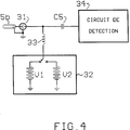
- FIG. 4 A partial diagram of the processing unit 6 is shown in FIG. 4.
- the screened cable 56 is connected to an input 31 of the processing unit 6.
- a generator 32 of direct voltage is connected to the input 31 through an inductor 33 which stops the alternating currents and allows the direct current to pass.
- the generator 32 supplies the input 31 with a first voltage V1 in normal operating mode and a second voltage V2, different from the first, in test mode.
- the voltages V1 and V2 are used to supply and control the test of the preamplification device 9.
- a detection circuit 34 is connected to the input 31 through a capacitor C5 which allows the signals coming from the coupler 13 to pass and blocks the DC component of the supply supplied by the generator 32.
- the detection circuit 34 comprising filters , separates the signals from the amplification circuit 11 and the signals supplied by the oscillator 12. Then, said signals are analyzed, in a known manner, to detect the presence of electric discharges and insulation faults.
- the preamplification device 9 connected to the antenna 4 can be installed outside the tank 3 as in Figure 2 to be easily interchangeable.
- the device is installed inside the tank 3 so as to reduce the distance between the antenna and the circuits 11 and 12.
- the assembly constituted by the antenna 4 and the preamplification device 9 forms an active antenna with high efficiency having a good signal to noise ratio.
- the high-pass and low-pass filters are represented as separate components, although it is quite possible to integrate them into the amplifier circuits or into the coupler 13.
- the pass-through filters high and low pass can also be replaced by band pass filters.
- the noise generator 20 has the advantage of covering a very wide frequency band, but any other signal generator can be used.
- the base frequency of the voltage-controlled oscillator 24 given as an example is 10 MHz, but any other value greater than the network frequency could be suitable.
Landscapes
- Physics & Mathematics (AREA)
- General Physics & Mathematics (AREA)
- Testing Relating To Insulation (AREA)
- Arc-Extinguishing Devices That Are Switches (AREA)
Applications Claiming Priority (2)
| Application Number | Priority Date | Filing Date | Title |
|---|---|---|---|
| FR9407616 | 1994-06-20 | ||
| FR9407616A FR2721408B1 (fr) | 1994-06-20 | 1994-06-20 | Dispositif de détection de décharges électriques pour appareillage électrique. |
Publications (1)
| Publication Number | Publication Date |
|---|---|
| EP0689059A1 true EP0689059A1 (de) | 1995-12-27 |
Family
ID=9464480
Family Applications (1)
| Application Number | Title | Priority Date | Filing Date |
|---|---|---|---|
| EP95410056A Withdrawn EP0689059A1 (de) | 1994-06-20 | 1995-06-13 | Teilentladungsdetektor für elektrische Anlagen |
Country Status (3)
| Country | Link |
|---|---|
| EP (1) | EP0689059A1 (de) |
| JP (1) | JPH0817298A (de) |
| FR (1) | FR2721408B1 (de) |
Families Citing this family (3)
| Publication number | Priority date | Publication date | Assignee | Title |
|---|---|---|---|---|
| RU2207581C2 (ru) * | 2001-04-17 | 2003-06-27 | Марийский государственный университет | Способ определения состояния линейной изоляции распределительных сетей и определения места её повреждения |
| JP5198026B2 (ja) * | 2007-10-10 | 2013-05-15 | シャープ株式会社 | 高電圧放電部の動作確認方法及び装置 |
| RU2365928C1 (ru) * | 2007-12-03 | 2009-08-27 | Государственное образовательное учреждение высшего профессионального образования Иркутский государственный университет путей сообщения (ИрГУПС(ИрИИТ)) | Способ дистанционной акустоэлектромагнитной диагностики состояния линейной изоляции контактной сети переменного тока железнодорожного транспорта |
Citations (4)
| Publication number | Priority date | Publication date | Assignee | Title |
|---|---|---|---|---|
| EP0134187A2 (de) * | 1983-07-29 | 1985-03-13 | Siemens Aktiengesellschaft | Messvorrichtung zur Feststellung von Teilentladungen innerhalb metallgekapselter, druckgasisolierter Hochspannungsschaltanlagen |
| DE3816047A1 (de) * | 1988-04-19 | 1989-11-02 | Inst Energieversorgung | Schaltungsanordnung zur akustischen teilentladungsdetektion |
| EP0342597A2 (de) * | 1988-05-16 | 1989-11-23 | Hitachi, Ltd. | Abnormitäts-Diagnosesystem für eine Hochspannungsanlage |
| EP0488719A2 (de) * | 1990-11-30 | 1992-06-03 | Kabushiki Kaisha Toshiba | System und Methode zur Detektion von Teilentladungen von gasisolierten Schaltern |
-
1994
- 1994-06-20 FR FR9407616A patent/FR2721408B1/fr not_active Expired - Fee Related
-
1995
- 1995-06-13 EP EP95410056A patent/EP0689059A1/de not_active Withdrawn
- 1995-06-20 JP JP15362995A patent/JPH0817298A/ja active Pending
Patent Citations (4)
| Publication number | Priority date | Publication date | Assignee | Title |
|---|---|---|---|---|
| EP0134187A2 (de) * | 1983-07-29 | 1985-03-13 | Siemens Aktiengesellschaft | Messvorrichtung zur Feststellung von Teilentladungen innerhalb metallgekapselter, druckgasisolierter Hochspannungsschaltanlagen |
| DE3816047A1 (de) * | 1988-04-19 | 1989-11-02 | Inst Energieversorgung | Schaltungsanordnung zur akustischen teilentladungsdetektion |
| EP0342597A2 (de) * | 1988-05-16 | 1989-11-23 | Hitachi, Ltd. | Abnormitäts-Diagnosesystem für eine Hochspannungsanlage |
| EP0488719A2 (de) * | 1990-11-30 | 1992-06-03 | Kabushiki Kaisha Toshiba | System und Methode zur Detektion von Teilentladungen von gasisolierten Schaltern |
Also Published As
| Publication number | Publication date |
|---|---|
| FR2721408B1 (fr) | 1996-08-02 |
| JPH0817298A (ja) | 1996-01-19 |
| FR2721408A1 (fr) | 1995-12-22 |
Similar Documents
| Publication | Publication Date | Title |
|---|---|---|
| CA1255359A (en) | Control apparatus for the electronic detection in alternating current transmission lines of fault locations causing power losses | |
| KR101297901B1 (ko) | 전력선의 부분 방전의 검출 및 감시 | |
| US7746053B2 (en) | Tester for RF devices | |
| US20210190839A1 (en) | Device and method for processing partial discharge technical field | |
| KR102153448B1 (ko) | 광대역 무손실 부분방전 검출 및 노이즈 제거 장치 | |
| CH422984A (fr) | Appareil de mesure électrique | |
| EP2726888B1 (de) | Verfahren und vorrichtung zur steuerung einer gasisolierten elektrischen hochspannungsschaltanlage | |
| US12130316B2 (en) | Broadband lossless partial discharge detection and noise removal device | |
| CA1119702A (en) | Parametric frequency division | |
| EP0689059A1 (de) | Teilentladungsdetektor für elektrische Anlagen | |
| CA2304280C (en) | Frequency agile transponder | |
| EP0657742A2 (de) | Einrichtung zur Erkennung von Störlichtbögen in Energiekabeln | |
| FR2829622A1 (fr) | Systeme antennaire a rendement elevee et a forte puissance | |
| GB2236593A (en) | Electromagnetic field detector | |
| Showers et al. | Fundamental limits on EMC | |
| JPH03293908A (ja) | 絶縁監視用アンテナ装置 | |
| EP0745863A1 (de) | Elektronischen Entladungsdetektor für Elektrogeräte | |
| LU88828A1 (fr) | Dispositif de sondage d'un corps conducteur | |
| KR100670128B1 (ko) | 필터설계와 필터측정 기능을 갖는 전자파 분석 장치 | |
| US20230017123A1 (en) | Provider equipment identification | |
| Fridberg et al. | Upgrading and operating of the 80 MHz transmitter on the Alcator C-Mod tokamak | |
| Yao et al. | A new partial discharge detector | |
| JP2023125237A (ja) | 部分放電検出装置、及び部分放電検出方法 | |
| FR2679038A1 (fr) | Un appareil pour la mesure des caracteristiques vectorielles d'un signal electrique deporte module en amplitude. | |
| EP0576382A1 (de) | Übertragungsverfahren für elektrische Signale über einen Funkkanal und Übertragungssysteme zur Aufführung dieses Verfahrens |
Legal Events
| Date | Code | Title | Description |
|---|---|---|---|
| PUAI | Public reference made under article 153(3) epc to a published international application that has entered the european phase |
Free format text: ORIGINAL CODE: 0009012 |
|
| AK | Designated contracting states |
Kind code of ref document: A1 Designated state(s): CH DE GB IT LI SE |
|
| 17P | Request for examination filed |
Effective date: 19960529 |
|
| RAP1 | Party data changed (applicant data changed or rights of an application transferred) |
Owner name: SCHNEIDER ELECTRIC INDUSTRIES SA |
|
| RAP1 | Party data changed (applicant data changed or rights of an application transferred) |
Owner name: SCHNEIDER ELECTRIC HIGH VOLTAGE SA |
|
| STAA | Information on the status of an ep patent application or granted ep patent |
Free format text: STATUS: THE APPLICATION IS DEEMED TO BE WITHDRAWN |
|
| 18D | Application deemed to be withdrawn |
Effective date: 20021231 |