EP0689239A1 - Procédé de manufacture des dispositifs de puissance en technologie MOS - Google Patents
Procédé de manufacture des dispositifs de puissance en technologie MOS Download PDFInfo
- Publication number
- EP0689239A1 EP0689239A1 EP94830316A EP94830316A EP0689239A1 EP 0689239 A1 EP0689239 A1 EP 0689239A1 EP 94830316 A EP94830316 A EP 94830316A EP 94830316 A EP94830316 A EP 94830316A EP 0689239 A1 EP0689239 A1 EP 0689239A1
- Authority
- EP
- European Patent Office
- Prior art keywords
- layer
- insulated gate
- conductivity type
- semiconductor material
- material layer
- Prior art date
- Legal status (The legal status is an assumption and is not a legal conclusion. Google has not performed a legal analysis and makes no representation as to the accuracy of the status listed.)
- Granted
Links
Images


Classifications
-
- H—ELECTRICITY
- H10—SEMICONDUCTOR DEVICES; ELECTRIC SOLID-STATE DEVICES NOT OTHERWISE PROVIDED FOR
- H10D—INORGANIC ELECTRIC SEMICONDUCTOR DEVICES
- H10D30/00—Field-effect transistors [FET]
- H10D30/01—Manufacture or treatment
- H10D30/021—Manufacture or treatment of FETs having insulated gates [IGFET]
- H10D30/028—Manufacture or treatment of FETs having insulated gates [IGFET] of double-diffused metal oxide semiconductor [DMOS] FETs
- H10D30/0291—Manufacture or treatment of FETs having insulated gates [IGFET] of double-diffused metal oxide semiconductor [DMOS] FETs of vertical DMOS [VDMOS] FETs
-
- H—ELECTRICITY
- H10—SEMICONDUCTOR DEVICES; ELECTRIC SOLID-STATE DEVICES NOT OTHERWISE PROVIDED FOR
- H10D—INORGANIC ELECTRIC SEMICONDUCTOR DEVICES
- H10D30/00—Field-effect transistors [FET]
- H10D30/60—Insulated-gate field-effect transistors [IGFET]
- H10D30/64—Double-diffused metal-oxide semiconductor [DMOS] FETs
- H10D30/66—Vertical DMOS [VDMOS] FETs
-
- H—ELECTRICITY
- H10—SEMICONDUCTOR DEVICES; ELECTRIC SOLID-STATE DEVICES NOT OTHERWISE PROVIDED FOR
- H10D—INORGANIC ELECTRIC SEMICONDUCTOR DEVICES
- H10D62/00—Semiconductor bodies, or regions thereof, of devices having potential barriers
- H10D62/10—Shapes, relative sizes or dispositions of the regions of the semiconductor bodies; Shapes of the semiconductor bodies
- H10D62/17—Semiconductor regions connected to electrodes not carrying current to be rectified, amplified or switched, e.g. channel regions
- H10D62/393—Body regions of DMOS transistors or IGBTs
-
- H—ELECTRICITY
- H10—SEMICONDUCTOR DEVICES; ELECTRIC SOLID-STATE DEVICES NOT OTHERWISE PROVIDED FOR
- H10P—GENERIC PROCESSES OR APPARATUS FOR THE MANUFACTURE OR TREATMENT OF DEVICES COVERED BY CLASS H10
- H10P30/00—Ion implantation into wafers, substrates or parts of devices
- H10P30/20—Ion implantation into wafers, substrates or parts of devices into semiconductor materials, e.g. for doping
- H10P30/22—Ion implantation into wafers, substrates or parts of devices into semiconductor materials, e.g. for doping using masks
- H10P30/221—Ion implantation into wafers, substrates or parts of devices into semiconductor materials, e.g. for doping using masks characterised by the angle between the ion beam and the mask
-
- H—ELECTRICITY
- H10—SEMICONDUCTOR DEVICES; ELECTRIC SOLID-STATE DEVICES NOT OTHERWISE PROVIDED FOR
- H10P—GENERIC PROCESSES OR APPARATUS FOR THE MANUFACTURE OR TREATMENT OF DEVICES COVERED BY CLASS H10
- H10P30/00—Ion implantation into wafers, substrates or parts of devices
- H10P30/20—Ion implantation into wafers, substrates or parts of devices into semiconductor materials, e.g. for doping
- H10P30/222—Ion implantation into wafers, substrates or parts of devices into semiconductor materials, e.g. for doping characterised by the angle between the ion beam and the crystal planes or the main crystal surface
Definitions
- the present invention relates to a zero thermal budget manufacturing process for MOS-technology power devices, such as power MOSFETs and Insulated Gate Bipolar Transistors (IGBTs).
- MOS-technology power devices such as power MOSFETs and Insulated Gate Bipolar Transistors (IGBTs).
- MOS-technology power devices are made up of a plurality of elementary functional units connected in parallel to conduct each one a respective fraction of the overall power device current.
- Each elementary unit comprises a so-called "body region” of one conductivity type (P type for an N-channel device), formed in a lightly doped semiconductor layer of an opposite conductivity type (N type) common to all the functional units; a heavily doped source region of said opposite conductivity type (N type) is provided inside the body region; the portion of the body region comprised between the source region and the edge of the body region itself is covered by a thin oxide layer (called “gate oxide”) and by a polysilicon layer (“gate layer”), and forms a channel region of the elementary functional unit.
- the source regions of all the elementary functional units are contacted by a same metal layer constituting a source electrode of the power device.
- the body regions have a square plan, and the power device is made up of a bidimensional array of square-plan elementary cells.
- the body region comprises a central heavily doped region (sometimes called “deep body region”) and a lateral lightly doped channel region;
- the source region has an annular shape and is formed in said lateral channel region, substantially around the deep body region.
- the source metal layer which contacts the source region also contacts the deep body region of the elementary cells, to short-circuit the base-emitter junction of a parasitic bipolar junction transistor (BJT) having emitter, base and collector respectively represented by the source region, the portion of the body region under the source region, and the lightly doped semiconductor layer (an NPN transistor in the case of an N-channel power device).
- BJT parasitic bipolar junction transistor
- a conventional manufacturing process provides for:
- the doping level of the deep body regions must be suitable to obtain low-resistance contact regions for the body regions, while the doping level of the channel regions is adjusted on the basis of the threshold voltage value desired for the power device; typical implantation doses are in the range of 1013-1014 atoms/cm2 for the channel regions, and 1015 atoms/cm2 for the deep body regions.
- Three distinct masks are necessary to introduce the dopants for the various regions of the elementary cells.
- the windows opened in the implantation mask for the deep body regions are smaller than the windows opened by etching in the polysilicon and oxide layers, to avoid that the lateral diffusion of the deep body regions during the several thermal steps alters the doping profile of the channel regions.
- the source regions are implanted in a self-aligned way with the edges of the windows in the polysilicon and thin oxide layers, but the implantation mask must further provide unexposed surface regions in the middle of the deep body regions.
- the source region extends for a significant part in the channel region. Since the channel region has a relatively high sheet resistance (in the range of 600 ohm/square), the short-circuit of the base-emitter junction of the parasitic bipolar transistor becomes less effective with the increase in the lateral distance from the deep body region (a resistor is in fact introduced between the emitter and the base regions of the parasitic transistor, its breakdown voltage lowers, and the breakdown voltage of the power device is consequently lowered). It would be therefore desirable to make the deep body region extend as far as possible under the source region. The problem is that, due to the lateral diffusion of the deep body region dopants during the thermal steps of the fabrication process, the doping profile in the channel region could be altered. Thus, in conventional MOS-technology power devices, the region near the edge of the source region to the channel region of the elementary cells is critical from the point of view of the parasitic transistor triggering on.
- Such a process not only require one mask less than the conventional process, but also allows to obtain source regions almost completely included in the heavily doped portion of the body regions, so that the base series resistance of the parasitic BJT is quite small along all the source region.
- the thickness of the gate oxide cannot be scaled down below 350-500 Angstroms.
- the channel legth is inevitably high (typically about 1 ⁇ m); long channels mean low conductivity and thus high "on" resistances.
- the lateral diffusion technique used for the formation of the channel its dopant concentration decreases moving along it, and the channel resistance increases.
- a main object of the present invention is to provide a manufacturing process for MOS-technology power devices, suitable to obtain structures less affected by the abovementioned problems.
- the deep body and channel portions of the body regions are formed just by implantation, without thermal diffusion steps; the channel regions of the elementary functional units can thus be made shorter than in conventional processes: the dopants are in fact placed just where they are requested, and in the desired concentration, by adjusting the implantation energy and dose. The dimensions of the channel regions are thus highly controlled.
- the gate oxide thickness can be reduced from the current 350-500 Angstroms to 100-200 Angstroms. For the same reason, junction depths are smaller, so that thinner epitaxial layers can be grown: this results in a decrease of the "on" resistance of the power device.
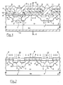
- FIG. 1 a cross-section of a MOS-technology power device is shown, more precisely a power MOSFET.
- the power MOSFET is made up of a plurality of elementary functional units 1 each comprising a P type body region 2 formed in a lightly doped N type ("N-") epitaxial layer 3 grown over a heavily doped N type (“N+”) substrate 4.
- the elementary functional units are for example represented by square-plan elementary cells.
- the P type body region 2 of each elementary cell 1 comprises a first, heavily doped ("P+”) portion 5, and a second, more lightly doped ("P-") lateral portion 6 forming a channel region of the elementary cell 1.
- Each cell 1 also comprises an N+ source region 7 formed in the heavily doped portion 5 of the body region 2 and having an annular shape, with a hole in the middle.
- An insulated gate layer 8 comprising a thin gate oxide layer 9 and a polysilicon gate layer 10, extends between adjacent elementary cells 1 and covers the surface of the channel region 6 of the body region 2.
- the heavily doped portion 5 of the body region and the source region 7 are both substantially aligned with the edges of the insulated gate layer 8.
- the insulated gate layer 8 is covered by an insulation layer 11, such as the so-called "PVapox", in which contact windows 12 are opened over the source region 7 and the heavily doped portion 5 of the body region 2 to allow a superimposed metal layer 13 to contact them.
- the metal layer 13 contacts in the same way all the elementary cells, and forms a source electrode S of the power MOSFET.
- a drain electrode D is also formed by covering the bottom surface of the substrate 4 by a metal layer 14.
- the base series resistance of the parasitic vertical BJT having emitter and base represented by the source region 7 and the underlying portion of the body region 2 is negligible even near the external edge of the source region.
- the base/emitter junction of such parasitic BJT is thus effectively short-circuited by the metal layer 13, to prevent it from being triggered on.
- the breakdown voltage of the power MOSFET is thus not reduced.
- a manufacturing process according to the present invention starts with the epitaxial growth of a lightly doped N type layer 3 over a heavily doped N type substrate 4.
- the surface of the N- layer 3 is then covered by a thin gate oxide layer 9 (e.g. thermally grown); the gate oxide layer 9 can be as thin as 100-200 Angstroms.
- a polysilicon gate layer 10 is then formed (e.g. by deposition) over the gate oxide layer 9. The two layers 9 and 10 form an insulated gate layer 8 (Fig. 2).
- the insulated gate layer 8 (i.e. the polysilicon layer 10 and the gate oxide layer 9) is then selectively removed from the surface of the N- layer 3 to open a plurality of windows 30 (which, in the present example, have a square plan).
- This step is performed in a per-se known way by covering the insulated gate layer 8 with a photoresist 20, and removing it from the regions of the insulated gate layer surface which are to be exposed to the action of an etchant with high selectivity towards polysilicon and silicon dioxide with respect to the photoresist material (Fig. 3).
- a P type dopant (such as boron) is then selectively implanted into the N- layer 3 through the windows 30, the insulated gate layer 8 acting as a mask for the implanted dopant ions: the dopant distribution is thus laterally self-aligned with the edges of the insulated gate layer 8.
- the dopant dose and the implantation energy are chosen in such a way that, after the implantation, heavily doped regions 5 are obtained without any thermal diffusion step (Fig. 4); a suitable dopant dose can be 1014-1015 atoms/cm2; the implantation energy is such that the peak concentration is located at a prescribed distance from the surface of the N-layer 3.
- a P type dopant is selectively implanted into the N- layer 3 through the windows 30, tilting the dopant ion beam of an angle ⁇ 1 with respect to the direction orthogonal to the surface of the N- layer 3; this can be done using one of the commercially available implanters which, like the Eaton 8200 P, allow tilt angles ranging from 0° to approximately 60°; in the present example, a tilt angle in the range 35°-60°, preferably 45°, is suitable.
- the implantation mask is again provided by the insulated gate layer 8. The dopant ions are thus implanted under the thin oxide layer 9 in a region near one of the edges of the insulated gate layer 8 (Fig. 5).
- This step is then repeated tilting the dopant ion beam of an angle ⁇ 2, for example 45°, in the opposite sense, to implant the dopant ions under the thin oxide layer 9 in a region near the opposite edge of the insulated gate layer 8 (Fig. 6), and so on until the dopant has been implanted under all the edges of the insulated gate layer 8.
- ⁇ 2 for example 45°
- ⁇ 6 the dopant ion beam
- the dopant dose and the implantation energy are chosen on the basis of the desired threshold voltage of the power MOSFET, and of the desired channel length; a suitable dose is for example 1012-1013 atoms/cm2 and the implantation energy can be of 100-200 KeV. It is to be noted that the channel regions 6 do not extend around the corners of the windows 30.
- a heavy dose of an N type dopant is then selectively introduced into the heavily doped regions 5, for example by ion implantation; the implantion mask is provided in part by the insulated gate layer 8, but must further comprise photoresist isles 22 in the middle of the heavily doped regions 5 to prevent the ions from being implanted in the central portions of the regions 5 which will be contacted by a metal layer (Fig. 7). It is also necessary to prevent the N type dopant from being implanted near the corners of the windows 30 in the insulated gate layer 8, to avoid the source regions 7 being in direct contact with the N- layer 3 (this would cause a source-drain short-circuit). This can be done by covering the four corners of the windows 30 with a phootoresist. Annular source regions 7, self-aligned with the insulated gate layer 8 and substantially internal to the heavily doped regions 5, are thus formed.
- a high temperature, low time duration thermal step is at this point performed to activate the dopants and to partially remove defects caused by the implantation of dopants.
- Such step is performed in Rapid Thermal Annealers (RTAs), and does not cause significant dopant redistribution; the doping profiles and dimensions of the various regions of the elementary cells 1 are thus not affected.
- RTAs Rapid Thermal Annealers
- An insulation layer 11 is formed over the insulated gate layer 8, and it is selectively removed to open contact windows 12 over the elementary cells.
- the insulation layer 11 is covered by a metal layer 13 which contacts the source region 7 and the heavily doped region 5 of all the elementary cells 1.
- a metal layer 14 is also formed on the bottom surface of the N+ substrate 4.
- the manufacturing process according to the invention has a further distinct advantage over the conventional processes. It is known that the power MOSFET breakdown voltage depends on the thickness t of the portion of the N- layer 3 between the N+ substrate 4 and the P+ regions 5: by way of example, for low-voltage devices which must withstand 60 V between drain and source, such portion must be at least 3.5 ⁇ m thick; since in conventional processes the depth d of the heavily doped regions 5 is not less than 4 ⁇ m, an epitaxial layer of at least 7.5 ⁇ m thickness (t+d) is necessary.
- the process according to the present invention instead, not involving thermal steps with high thermal budgets (i.e.
- the depth d of the junction between the heavily doped portions 5 of the body regions 2 and the N- layer 3 can be reduced to 0.6 ⁇ m: the overall thickness t+d of the epitaxial layer necessary to assure 60 V of breakdown voltage is thus reduced to 4.1 ⁇ m.
- the length of the so-called “vertical JFET” represented by the portion of the epitaxial layer comprised between the body region 2 of two adjacent elementary cells is thus reduced. From the one hand, this makes it possible to lower the "on" resistance of the power MOSFET.
- the process according to the present invention applies as well to the fabrication of IGBTs, the only difference being the conductivity type of the substrate 4.
- the process according to the present invention is not limited to MOS-technology power devices made up of arrays of square-plan elementary cells as those previously described, but extends to high-density devices made up of a plurality of elementary functional units wherein the body regions are elongated stripes with one dimension much greater than the other.
- Such a device is described in the co-pending European Patent Application No. 94830288.0.
- the windows 30 in the insulated gate layer 8 are substantially rectangular, with two sides much longer than the other.
- Channel regions 6 are present under the long edges of the insulated gate layer 8, so that their formation requires only two tilted implantation steps, instead of four.
Landscapes
- Insulated Gate Type Field-Effect Transistor (AREA)
Priority Applications (5)
| Application Number | Priority Date | Filing Date | Title |
|---|---|---|---|
| EP94830316A EP0689239B1 (fr) | 1994-06-23 | 1994-06-23 | Procédé de manufacture des dispositifs de puissance en technologie MOS |
| DE69434937T DE69434937D1 (de) | 1994-06-23 | 1994-06-23 | Verfahren zur Herstellung von Leistungsbauteilen in MOS-Technologie |
| US08/493,004 US5933733A (en) | 1994-06-23 | 1995-06-21 | Zero thermal budget manufacturing process for MOS-technology power devices |
| JP7155983A JP2618615B2 (ja) | 1994-06-23 | 1995-06-22 | Mos型電力装置の製造方法 |
| US08/856,109 US6140679A (en) | 1994-06-23 | 1997-05-14 | Zero thermal budget manufacturing process for MOS-technology power devices |
Applications Claiming Priority (1)
| Application Number | Priority Date | Filing Date | Title |
|---|---|---|---|
| EP94830316A EP0689239B1 (fr) | 1994-06-23 | 1994-06-23 | Procédé de manufacture des dispositifs de puissance en technologie MOS |
Publications (2)
| Publication Number | Publication Date |
|---|---|
| EP0689239A1 true EP0689239A1 (fr) | 1995-12-27 |
| EP0689239B1 EP0689239B1 (fr) | 2007-03-07 |
Family
ID=8218476
Family Applications (1)
| Application Number | Title | Priority Date | Filing Date |
|---|---|---|---|
| EP94830316A Expired - Lifetime EP0689239B1 (fr) | 1994-06-23 | 1994-06-23 | Procédé de manufacture des dispositifs de puissance en technologie MOS |
Country Status (4)
| Country | Link |
|---|---|
| US (2) | US5933733A (fr) |
| EP (1) | EP0689239B1 (fr) |
| JP (1) | JP2618615B2 (fr) |
| DE (1) | DE69434937D1 (fr) |
Cited By (1)
| Publication number | Priority date | Publication date | Assignee | Title |
|---|---|---|---|---|
| FR2767964A1 (fr) * | 1997-09-04 | 1999-03-05 | St Microelectronics Sa | Procede de realisation de la zone de canal d'un transistor dmos |
Families Citing this family (29)
| Publication number | Priority date | Publication date | Assignee | Title |
|---|---|---|---|---|
| US6025231A (en) * | 1997-02-18 | 2000-02-15 | Texas Instruments Incorporated | Self aligned DMOS transistor and method of fabrication |
| JP3429654B2 (ja) * | 1997-12-24 | 2003-07-22 | セイコーインスツルメンツ株式会社 | 半導体集積回路装置の製造方法 |
| US6707103B1 (en) * | 1998-03-05 | 2004-03-16 | International Rectifier Corporation | Low voltage rad hard MOSFET |
| DE19845003C1 (de) * | 1998-09-30 | 2000-02-10 | Siemens Ag | Vertikaler Feldeffekttransistor mit innenliegendem ringförmigen Gate und Herstellverfahren |
| DE69936175T2 (de) | 1998-11-04 | 2008-01-24 | Lucent Technologies Inc. | Induktivität oder Leiterbahn mit geringem Verlust in einer integrierten Schaltung |
| US6225182B1 (en) * | 1999-08-30 | 2001-05-01 | Agere Systems Guardian Corp. | Simplified high Q inductor substrate |
| US6174778B1 (en) * | 1998-12-15 | 2001-01-16 | United Microelectronics Corp. | Method of fabricating metal oxide semiconductor |
| US6624030B2 (en) | 2000-12-19 | 2003-09-23 | Advanced Power Devices, Inc. | Method of fabricating power rectifier device having a laterally graded P-N junction for a channel region |
| US20030030051A1 (en) | 2001-08-09 | 2003-02-13 | International Rectifier Corporation | Superjunction device with improved avalanche capability and breakdown voltage |
| US7107040B2 (en) * | 2002-02-11 | 2006-09-12 | The Chamberlain Group, Inc. | Method and apparatus for displaying blocked transmitter information |
| US6861303B2 (en) * | 2003-05-09 | 2005-03-01 | Texas Instruments Incorporated | JFET structure for integrated circuit and fabrication method |
| JP4437655B2 (ja) * | 2003-10-02 | 2010-03-24 | 三菱電機株式会社 | 半導体装置及び半導体装置の駆動回路 |
| US7166890B2 (en) | 2003-10-21 | 2007-01-23 | Srikant Sridevan | Superjunction device with improved ruggedness |
| KR100629605B1 (ko) * | 2004-12-31 | 2006-09-27 | 동부일렉트로닉스 주식회사 | 엘디모스 채널 형성 방법 |
| US7553734B2 (en) * | 2005-10-17 | 2009-06-30 | Princeton Lightwave, Inc. | Method for forming an avalanche photodiode |
| JP4812480B2 (ja) * | 2006-03-22 | 2011-11-09 | 富士通セミコンダクター株式会社 | 半導体装置の製造方法 |
| RU2361318C2 (ru) * | 2006-07-18 | 2009-07-10 | Федеральное Государственное Унитарное Предприятие "Научно-Производственное Предприятие "Пульсар" | Способ изготовления мощных полевых транзисторов с изолированным затвором |
| KR100770538B1 (ko) | 2006-08-09 | 2007-10-25 | 동부일렉트로닉스 주식회사 | 횡형 디모스 트랜지스터의 제조방법 |
| US8274128B2 (en) | 2007-03-23 | 2012-09-25 | Siliconix Technology C. V. Ir | Semiconductor device with buffer layer |
| US10226818B2 (en) * | 2009-03-20 | 2019-03-12 | Pratt & Whitney Canada Corp. | Process for joining powder injection molded parts |
| US8525257B2 (en) * | 2009-11-18 | 2013-09-03 | Micrel, Inc. | LDMOS transistor with asymmetric spacer as gate |
| US9722041B2 (en) | 2012-09-19 | 2017-08-01 | Vishay-Siliconix | Breakdown voltage blocking device |
| US9970318B2 (en) | 2014-06-25 | 2018-05-15 | Pratt & Whitney Canada Corp. | Shroud segment and method of manufacturing |
| DE102015118616B3 (de) * | 2015-10-30 | 2017-04-13 | Infineon Technologies Austria Ag | Latchup-fester Transistor |
| JP6687476B2 (ja) * | 2016-07-25 | 2020-04-22 | 株式会社日立製作所 | 半導体装置およびその製造方法 |
| US11205718B1 (en) * | 2018-11-26 | 2021-12-21 | Texas Instruments Incorporated | High performance super-beta NPN (SBNPN) |
| DE102020117171A1 (de) | 2020-06-30 | 2021-12-30 | Infineon Technologies Dresden GmbH & Co. KG | Lateral-transistor mit selbstausrichtendem body-implantat |
| CN112117193B (zh) * | 2020-09-21 | 2023-05-16 | 杭州芯迈半导体技术有限公司 | 碳化硅mosfet器件及其制造方法 |
| CN119153497A (zh) * | 2023-06-16 | 2024-12-17 | 苏州东微半导体股份有限公司 | 碳化硅器件及其制造方法 |
Citations (7)
| Publication number | Priority date | Publication date | Assignee | Title |
|---|---|---|---|---|
| US4417385A (en) * | 1982-08-09 | 1983-11-29 | General Electric Company | Processes for manufacturing insulated-gate semiconductor devices with integral shorts |
| EP0179407A2 (fr) * | 1984-10-25 | 1986-04-30 | STMicroelectronics S.r.l. | Procédé de fabrication d'un dispositif semi-conducteur du type DMOS |
| JPS6251216A (ja) * | 1985-08-30 | 1987-03-05 | Toshiba Corp | 半導体装置の製造方法 |
| JPS62131579A (ja) * | 1985-12-03 | 1987-06-13 | Nec Corp | 縦型電界効果トランジスタの製造方法 |
| JPH0465132A (ja) * | 1990-07-05 | 1992-03-02 | Oki Electric Ind Co Ltd | 二重拡散型mos fetの製造方法 |
| EP0481153A1 (fr) * | 1990-10-16 | 1992-04-22 | Consorzio per la Ricerca sulla Microelettronica nel Mezzogiorno - CoRiMMe | Méthode de fabrication de transistors MOS de puissance à courant vertical |
| JPH05129602A (ja) * | 1991-11-01 | 1993-05-25 | Sony Corp | Mis型半導体装置の製造方法 |
Family Cites Families (22)
| Publication number | Priority date | Publication date | Assignee | Title |
|---|---|---|---|---|
| US3461360A (en) * | 1965-06-30 | 1969-08-12 | Ibm | Semiconductor devices with cup-shaped regions |
| US4001860A (en) * | 1973-11-12 | 1977-01-04 | Signetics Corporation | Double diffused metal oxide semiconductor structure with isolated source and drain and method |
| US3909320A (en) * | 1973-12-26 | 1975-09-30 | Signetics Corp | Method for forming MOS structure using double diffusion |
| JPS5185381A (fr) * | 1975-01-24 | 1976-07-26 | Hitachi Ltd | |
| DE2703877C2 (de) * | 1977-01-31 | 1982-06-03 | Siemens Ag, 1000 Berlin Und 8000 Muenchen | MIS-Transistor von kurzer Kanallänge und Verfahren zu seiner Herstellung |
| JPS53102668A (en) * | 1977-02-18 | 1978-09-07 | Toshiba Corp | Manufacture for semiconductor device |
| US4705759B1 (en) * | 1978-10-13 | 1995-02-14 | Int Rectifier Corp | High power mosfet with low on-resistance and high breakdown voltage |
| US4593302B1 (en) * | 1980-08-18 | 1998-02-03 | Int Rectifier Corp | Process for manufacture of high power mosfet laterally distributed high carrier density beneath the gate oxide |
| US4680853A (en) * | 1980-08-18 | 1987-07-21 | International Rectifier Corporation | Process for manufacture of high power MOSFET with laterally distributed high carrier density beneath the gate oxide |
| JPS59920A (ja) * | 1982-06-23 | 1984-01-06 | Fujitsu Ltd | 半導体装置の製造方法 |
| US4716126A (en) * | 1986-06-05 | 1987-12-29 | Siliconix Incorporated | Fabrication of double diffused metal oxide semiconductor transistor |
| JPH0783122B2 (ja) * | 1988-12-01 | 1995-09-06 | 富士電機株式会社 | 半導体装置の製造方法 |
| JPH02239670A (ja) * | 1989-03-14 | 1990-09-21 | Fujitsu Ltd | 半導体装置 |
| JPH03105978A (ja) * | 1989-09-20 | 1991-05-02 | Hitachi Ltd | 半導体装置 |
| US4931408A (en) * | 1989-10-13 | 1990-06-05 | Siliconix Incorporated | Method of fabricating a short-channel low voltage DMOS transistor |
| JPH0831606B2 (ja) * | 1989-11-17 | 1996-03-27 | 株式会社東芝 | 大電力用半導体装置 |
| JPH03241747A (ja) * | 1990-02-20 | 1991-10-28 | Nissan Motor Co Ltd | 半導体装置の製造方法 |
| KR940004446B1 (ko) * | 1990-11-05 | 1994-05-25 | 미쓰비시뎅끼 가부시끼가이샤 | 반도체장치의 제조방법 |
| JP2632101B2 (ja) * | 1990-11-05 | 1997-07-23 | 三菱電機株式会社 | 半導体装置の製造方法 |
| US5404040A (en) * | 1990-12-21 | 1995-04-04 | Siliconix Incorporated | Structure and fabrication of power MOSFETs, including termination structures |
| US5268586A (en) * | 1992-02-25 | 1993-12-07 | North American Philips Corporation | Vertical power MOS device with increased ruggedness and method of fabrication |
| US5430314A (en) * | 1992-04-23 | 1995-07-04 | Siliconix Incorporated | Power device with buffered gate shield region |
-
1994
- 1994-06-23 EP EP94830316A patent/EP0689239B1/fr not_active Expired - Lifetime
- 1994-06-23 DE DE69434937T patent/DE69434937D1/de not_active Expired - Lifetime
-
1995
- 1995-06-21 US US08/493,004 patent/US5933733A/en not_active Expired - Lifetime
- 1995-06-22 JP JP7155983A patent/JP2618615B2/ja not_active Expired - Lifetime
-
1997
- 1997-05-14 US US08/856,109 patent/US6140679A/en not_active Expired - Lifetime
Patent Citations (7)
| Publication number | Priority date | Publication date | Assignee | Title |
|---|---|---|---|---|
| US4417385A (en) * | 1982-08-09 | 1983-11-29 | General Electric Company | Processes for manufacturing insulated-gate semiconductor devices with integral shorts |
| EP0179407A2 (fr) * | 1984-10-25 | 1986-04-30 | STMicroelectronics S.r.l. | Procédé de fabrication d'un dispositif semi-conducteur du type DMOS |
| JPS6251216A (ja) * | 1985-08-30 | 1987-03-05 | Toshiba Corp | 半導体装置の製造方法 |
| JPS62131579A (ja) * | 1985-12-03 | 1987-06-13 | Nec Corp | 縦型電界効果トランジスタの製造方法 |
| JPH0465132A (ja) * | 1990-07-05 | 1992-03-02 | Oki Electric Ind Co Ltd | 二重拡散型mos fetの製造方法 |
| EP0481153A1 (fr) * | 1990-10-16 | 1992-04-22 | Consorzio per la Ricerca sulla Microelettronica nel Mezzogiorno - CoRiMMe | Méthode de fabrication de transistors MOS de puissance à courant vertical |
| JPH05129602A (ja) * | 1991-11-01 | 1993-05-25 | Sony Corp | Mis型半導体装置の製造方法 |
Non-Patent Citations (4)
| Title |
|---|
| PATENT ABSTRACTS OF JAPAN vol. 11, no. 237 (E - 528) 4 August 1987 (1987-08-04) * |
| PATENT ABSTRACTS OF JAPAN vol. 11, no. 355 (E - 558) 19 November 1987 (1987-11-19) * |
| PATENT ABSTRACTS OF JAPAN vol. 16, no. 275 (E - 1219) 19 June 1992 (1992-06-19) * |
| PATENT ABSTRACTS OF JAPAN vol. 17, no. 504 (E - 1430) 10 September 1993 (1993-09-10) * |
Cited By (1)
| Publication number | Priority date | Publication date | Assignee | Title |
|---|---|---|---|---|
| FR2767964A1 (fr) * | 1997-09-04 | 1999-03-05 | St Microelectronics Sa | Procede de realisation de la zone de canal d'un transistor dmos |
Also Published As
| Publication number | Publication date |
|---|---|
| JPH0817849A (ja) | 1996-01-19 |
| JP2618615B2 (ja) | 1997-06-11 |
| US5933733A (en) | 1999-08-03 |
| EP0689239B1 (fr) | 2007-03-07 |
| US6140679A (en) | 2000-10-31 |
| DE69434937D1 (de) | 2007-04-19 |
Similar Documents
| Publication | Publication Date | Title |
|---|---|---|
| EP0689239B1 (fr) | Procédé de manufacture des dispositifs de puissance en technologie MOS | |
| US5795793A (en) | Process for manufacture of MOS gated device with reduced mask count | |
| EP0696054B1 (fr) | Procédé de manufacture des dispositifs de puissance à haute densité en technology MOS | |
| US6710400B2 (en) | Method for fabricating a high voltage power MOSFET having a voltage sustaining region that includes doped columns formed by rapid diffusion | |
| US5981998A (en) | Single feature size MOS technology power device | |
| JP4743744B2 (ja) | フローティングアイランド電圧維持層を有する半導体パワーデバイス | |
| US5342797A (en) | Method for forming a vertical power MOSFET having doped oxide side wall spacers | |
| US5817546A (en) | Process of making a MOS-technology power device | |
| US20030122188A1 (en) | High voltage power MOSFET having a voltage sustaining region that includes doped columns formed by trench etching and ion implantation | |
| EP1287552A1 (fr) | Procede de fabrication d'un mosfet de puissance | |
| JPH08250731A (ja) | 高いブレークダウン電圧と低いオン抵抗を兼ね備えたトレンチ型mosfet | |
| EP0689238B1 (fr) | Procédé de manufacture d'un dispositif de puissance en technologie MOS | |
| US4735914A (en) | FET for high reverse bias voltage and geometrical design for low on resistance | |
| US5970343A (en) | Fabrication of conductivity enhanced MOS-gated semiconductor devices | |
| US6847094B2 (en) | Contact structure on a deep region formed in a semiconductor substrate | |
| AU698654C (en) | Process for manufacture of mos gated device with reduced mask count |
Legal Events
| Date | Code | Title | Description |
|---|---|---|---|
| PUAI | Public reference made under article 153(3) epc to a published international application that has entered the european phase |
Free format text: ORIGINAL CODE: 0009012 |
|
| AK | Designated contracting states |
Kind code of ref document: A1 Designated state(s): DE FR GB IT |
|
| 17P | Request for examination filed |
Effective date: 19960423 |
|
| 17Q | First examination report despatched |
Effective date: 19980206 |
|
| RAP3 | Party data changed (applicant data changed or rights of an application transferred) |
Owner name: CONSORZIO PER LA RICERCA SULLA MICROELETTRONICA N Owner name: STMICROELECTRONICS S.R.L. |
|
| RAP1 | Party data changed (applicant data changed or rights of an application transferred) |
Owner name: CONSORZIO PER LA RICERCA SULLA MICROELETTRONICA N Owner name: STMICROELECTRONICS S.R.L. |
|
| APAB | Appeal dossier modified |
Free format text: ORIGINAL CODE: EPIDOS NOAPE |
|
| APAB | Appeal dossier modified |
Free format text: ORIGINAL CODE: EPIDOS NOAPE |
|
| APAD | Appeal reference recorded |
Free format text: ORIGINAL CODE: EPIDOS REFNE |
|
| GRAP | Despatch of communication of intention to grant a patent |
Free format text: ORIGINAL CODE: EPIDOSNIGR1 |
|
| GRAS | Grant fee paid |
Free format text: ORIGINAL CODE: EPIDOSNIGR3 |
|
| APAF | Appeal reference modified |
Free format text: ORIGINAL CODE: EPIDOSCREFNE |
|
| GRAA | (expected) grant |
Free format text: ORIGINAL CODE: 0009210 |
|
| AK | Designated contracting states |
Kind code of ref document: B1 Designated state(s): DE FR GB IT |
|
| REG | Reference to a national code |
Ref country code: GB Ref legal event code: FG4D |
|
| REF | Corresponds to: |
Ref document number: 69434937 Country of ref document: DE Date of ref document: 20070419 Kind code of ref document: P |
|
| PLBE | No opposition filed within time limit |
Free format text: ORIGINAL CODE: 0009261 |
|
| STAA | Information on the status of an ep patent application or granted ep patent |
Free format text: STATUS: NO OPPOSITION FILED WITHIN TIME LIMIT |
|
| PG25 | Lapsed in a contracting state [announced via postgrant information from national office to epo] |
Ref country code: DE Free format text: LAPSE BECAUSE OF FAILURE TO SUBMIT A TRANSLATION OF THE DESCRIPTION OR TO PAY THE FEE WITHIN THE PRESCRIBED TIME-LIMIT Effective date: 20070609 |
|
| 26N | No opposition filed |
Effective date: 20071210 |
|
| PG25 | Lapsed in a contracting state [announced via postgrant information from national office to epo] |
Ref country code: IT Free format text: LAPSE BECAUSE OF FAILURE TO SUBMIT A TRANSLATION OF THE DESCRIPTION OR TO PAY THE FEE WITHIN THE PRESCRIBED TIME-LIMIT Effective date: 20070307 |
|
| PGFP | Annual fee paid to national office [announced via postgrant information from national office to epo] |
Ref country code: GB Payment date: 20130527 Year of fee payment: 20 |
|
| PGFP | Annual fee paid to national office [announced via postgrant information from national office to epo] |
Ref country code: FR Payment date: 20130724 Year of fee payment: 20 |
|
| REG | Reference to a national code |
Ref country code: GB Ref legal event code: PE20 Expiry date: 20140622 |
|
| PG25 | Lapsed in a contracting state [announced via postgrant information from national office to epo] |
Ref country code: GB Free format text: LAPSE BECAUSE OF EXPIRATION OF PROTECTION Effective date: 20140622 |